The future
Bạn đang xem bản rút gọn của tài liệu. Xem và tải ngay bản đầy đủ của tài liệu tại đây (248.6 KB, 13 trang )
Chapter 10: The Future
The previous chapters have focused on tools and techniques that you need to do
your job today. This chapter looks beyond the job as it is today to the future. First,
I want to describe a new technology — reconfigurable hardware — that has the
potential to completely redefine the process of creating an embedded system.
The closing half of this chapter is devoted not so much to what might come, as to
what I heartily wish would come.
Reconfigurable Hardware
The ultimate solution to the partitioning problem might be a new technology
known as reconfigurable hardware. Reconfigurable hardware might be the future of
computing systems in general, whether they are desktop PCs or embedded
systems. Reconfigurable hardware is circuitry that can be changed dynamically so
that its very structure changes at run time.
Imagine, for example, a microcontroller that consists of a standard microprocessor
core, a big block of this reconfigurable hardware, and nothing else. Unlike current
SoC solutions, this imaginary part wouldn’t include any dedicated peripheral
devices, such as timers, parallel ports, serial ports, Ethernet ports, and so on.
Instead, when the application calls for a parallel port, part of the reconfigurable
logic would be configured to be a parallel port. If a serial port is needed, the same
thing happens. If the design requires high-speed data steering logic, as you might
find in a telecommunications application, the hardware block is reconfigured to be
a steering block.
What is this magic hardware? The basis of this “brave new world” of computing
hardware is a device that has been around for more than 10 years, the Field
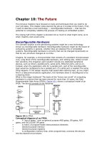
Programmable Gate Array (FPGA). Figure 10.1
shows a conceptual model of an
FPGA. The device consists of the following:
Figure 10.1: FPGA.
Conceptual diagram of an FPGA.
A “sea of gates,” such as general purpose AND gates, OR gates, NOT
gates, and EXCLUSIVE OR gates
A matrix of programmable interconnection elements
General-purpose memory
General-purpose registers
A configuration memory that, when programmed, connects the devices
into the desired circuit blocks
In Figure 10.1 each element from the sea of gates is represented by a traditional
logic gate. In actuality, FPGAs do not implement the logic function as traditional,
dedicated gates. Instead each individual logic element is actually a small
read/write memory array that is programmed directly with the desired function’s
truth table.
Figure 10.2
shows how this structure can be used to implement a simple AND gate.
In this representation, a and b are the address bits to the memory cells. The
output, x, is just the data bit stored in each memory cell. Thus, the AND gate can
be generated by a simple, four-cell memory that contains the following stored data:
ADDR(0,0) = 0ADDR(0,1) = 0ADDR(1,0) = 0ADDR(1,1) = 1
Figure 10.2: Gates.
Representing an AND function in a logic design.
With the logic table stored directly in the memory array, the output is TRUE, or 1,
if and only if both inputs are TRUE. Of course, this structure easily can be
expanded to functions with more than just two inputs. For example, you could
have an n-input AND gate, and output would be TRUE if, and only if, all n-input
variables were TRUE.
In real life, these memory arrays have five or six input variables each and two or
more independent output variables. The advantage of this approach is that any
logical expression that can be represented as a function of five or six independent
input variables can be programmed into each logic cell array.
Figure 10.3
shows the pieces in more detail. The unlabeled, small gray squares are
programmable cross-point switches, the key elements of the interconnection
matrix of Figure 10.1
. Each switch can be programmed to connect a vertical signal
wire to a horizontal signal wire by programming the corresponding control bit in
the configuration memory. The circuit block labeled “D Latch or FF” is the
elemental version of a register. Sending the appropriate clock signal or logic level
to the block causes the output of the logic cell array to be stored in the register.
Thus, as every electrical engineering student must realize by now, you have all the
elements that are necessary to build hardware state machines.
Figure 10.3: Interconnecting Elements of FPGA.
Interconnecting elements of the FPGA.
FPGA technology is not particularly new to hardware design. FPGAs have been
used for more than 10 years as a prototype part in the design of ASICs and other
custom-made integrated circuits (ICs). The advantage was that an FPGA could be
substituted for the actual IC until the correct hardware performance could be
verified, and then the FPGA-based design would be transferred to the silicon
manufacturer for production. Some silicon manufacturers were even able to read
the FPGA configuration files and generate the ASIC directly from that.
The early use of FPGAs was limited because the algorithms used to route the
device were slow and computationally intensive. It would commonly take a week of
computer time to find a route (correct configuration file) for a particularly dense
FPGA design. As the use of the FPGA’s resources rose above 50 to 60 percent, the
routing time began to increase dramatically. So even if an FPGA has a theoretical
capacity of 1,000 gates, perhaps a real design of less than 700 gates would
actually be able to fit into the device.
Another problem was cost. FPGAs were five to 10 times more costly than an
equivalent size ASIC, so production use was prohibitively expensive. However,
many applications were found that were not particularly cost sensitive, and the use
of the devices increased rapidly. Several new companies formed that arranged
large matrices of individual FPGAs to create equivalent FPGAs of much larger
capacity, in one case, over a million equivalent gates[3].
This imaginary processor plus reconfigurable hardware isn’t all imaginary. In 1998,
a new company called Triscend[2] introduced a microcontroller based on the
industry-standard 8032 that contained an array of reconfigurable elements. At the
September 2000, Embedded Systems Conference, the leading FPGA manufacturer,
Xilinx (www.xilinx.com
), announced that standard RISC cores would be available
for its FPGAs.
Today, we are just at the threshold of finding new and exciting ways to use the
concepts of reconfigurable hardware. Almost all modern embedded processors
contain dedicated blocks of circuitry for debugging the application and for
performance measurements in some cases. This circuitry is carried by every
processor that is shipped to a customer, even if the design was completed many
thousands of shipments ago. If the debug core was implemented in reconfigurable
hardware, the chip real-estate now “wasted” on debug logic could become
available for “soft” field hardware upgrades. There would be a limitless opportunity
to load specialized hardware into the arrays as needed.
In Chapter 3
, I discussed partitioning an embedded system between hardware
(fast but inflexible) and software (slower but flexible). The technology of
reconfigurable hardware now blurs this distinction even further. Researchers at HP
Laboratories[1] have shown that specialized computational hardware, even
running at modest speeds, such as 1MHz, can often outperform the capabilities of
supercomputers running thousands of times faster.
Now, factor in the reality that in the near future most embedded systems will be
attached to some distributed system, such as the Internet. Suppose you have
thousands of Internet appliances on a network. You want to measure various types
of performance parameters of your system as it runs during actual use. For a given
node in the system, there might be 20 separate and distinctive measurements that
you want to make at various times. Rather than design the specialized hardware
for each of these separate measurements, you could simply download
measurement configurations to the appliance via the Internet and then collect the
data locally. After the data is uploaded, you could then download another
measurement configuration.
Finally, really let your mind expand. With reconfigurable hardware, the entire
embedded system is designed and controlled as a software image. Today, several
vendors of IP-based microprocessor cores have parameterized their designs so
that much of the architecture of the microprocessor is user configurable. Why not
use the flexibility of reconfigurable hardware to enable a next-generation compiler
to compile a source file into the traditional software image and into the optimal
hardware configuration to execute the code most efficiently?
In today’s press, one can read article after article discussing the advantages of
DSPs and RISC in embedded applications. SoC designers are combining multiple
DSP and RISC cores in their latest designs. With reconfigurable hardware, the
distinctions among RISC, CISC, and DSP can go away completely. Just load the
correct hardware configuration that is needed at that point in time. It’s easy to do
because it’s only software.
Some Comments on the Tool Business
As someone involved in the development tool side of embedded systems for many
years I’ve had my share of frustrations trying to build tool chains that benefited
both the customers, the tool vendors and semiconductor manufacturers. It is clear
that the semiconductor vendors don’t always supply the quality of development
tools that they could. This is not meant as a criticism of the semiconductor
companies per se. For the semiconductor vendors, support tools represent the cost
of doing business. Tools exist to sell silicon. Without support tools you can’t sell
your silicon to the embedded designers who design your silicon into their products.
However, if you bear with me for a few pages and indulge me a little trip into the
land of fiction, I’ll try to paint you a picture of how it could be if tools really did
become a competitive edge. I should also give credit to the semiconductor
companies and tool vendors because almost all of the products that I’ll describe in
my little story already exist in one form or another.
Our story opens in a small, windowless conference room at ComDelta, a leading
supplier of LAN communications hardware and software for the rapidly growing
wireless-network industry. Sue Mason, one of the founders of ComDelta and its
chief hardware designer/system architect, is meeting with her design team to
discuss the requirements for ComDelta’s next-generation product. The model
CD700 is going to be ComDelta’s flagship wireless LAN bridge, servicing 100
simultaneous users.
The team is at a major decision point. Should they move to a higher performance
RISC processor from Integrated Micro Everything (IME) or attempt to squeeze
their existing 68060 design one more time? Clearly, using the Im46880 would
enable them to easily meet their feature set goals but as Ralph, the software team
leader, says, “Trying to do a software schedule with a 46880 processor would be a
joke. Garbage in, garbage out. We spent years getting to know the best way to
design for the 68K architecture. We know all the tools and their warts. And, to top
it off, we’ve got to have a prototype running by the Wireless World conference
next spring. No way!”
Sue had to admit that Ralph was right. In fact, as the only hardware designer
supporting a team of nine computer scientists and firmware engineers (EE
retreads), she wasn’t so sure that she could learn enough about the Im46K family
to have hardware for them when they needed it.
The uneasy silence was broken by Chin Lei, the newest employee of ComDelta and
a Cornell graduate with an MS/CS degree, who says, “I did my Master’s thesis on a
graphics engine design that used a bunch of Im46840s tied together. I was really
impressed with the way IME supported our efforts. Here we were, a bunch of
university geeks, and they treated us like we were some big laser printer company.
Not only that, their embedded design tools are first-rate, and their application
literature helped us understand the chip and design requirements. I wrote the
multiprocessor OS, and there was this IME software performance superguru, Jerry
Flemming, who wouldn’t let me screw up. I didn’t always understand him, but he
meant well. Those guys really have their act together.”
Sue went for a walk around the building, thinking about their dilemma. After about
an hour, she went back inside and spent the rest of the afternoon doing
administrivia. As she peddled home, she continued to think about Chin’s obvious
enthusiasm for IME.
The next morning, Sue called the local IME sales office. When Sue identified her
company, the IME Sales Administrator for the region checked it against her online
database of IME’s targeted accounts. ComDelta was one of the hot new companies
that IME wanted to penetrate. Her call was put through to the field sales engineer
for that account, and an automatic request was transmitted to IME’s headquarters
in Oregon for the ComDelta company profile.
As Ed Rosen spoke with Sue, he entered her data onto his computer. He focused
his questions on her knowledge of the Im46K product family and ComDelta’s time-
to-market needs. He clicked on the box that caused a Im46K Knowledge Box and
an Im46880 Evaluation Kit to be rushed to Sue and several other members of her
design team. It also started a chain of events in Portland and the IME Field Sales
Office. These events culminated in a presentation that Ed hoped to make at
ComDelta in the near future.
At work the following day, when Sue opened the Knowledge Box, some clever
packaging caused a DVD to rise to the top. “Watch me first” it said in bold letters.
Sue slipped the DVD into her drive. It presented an overview of how a team of
designers, new to the Im46K, could become proficient in a minimum amount of
time. It went through the tool chain, recommending certain vendors for particular
embedded applications. Sue was impressed. “No hype. Just facts,” she thought.
The presentation suggested a path to follow to specify the design and identify key
areas. It also contained a set of metrics taken from other Im46880 designs.
Sue was particularly intrigued by the System Design Assistant (SDA) software
package in the Knowledge Box. SDA is a program based on some of the latest
work in expert systems technology. Through a set of questions about her design
requirements, SDA provided Sue with some general design parameters, system