Switch Level Modeling part 1
Bạn đang xem bản rút gọn của tài liệu. Xem và tải ngay bản đầy đủ của tài liệu tại đây (30.61 KB, 7 trang )
[ Team LiB ]
11.1 Switch-Modeling Elements
Verilog provides various constructs to model switch-level circuits. Digital circuits at
MOS-transistor level are described using these elements.
[1]
[1]
Array of instances can be defined for switches. Array of instances is described in
Section 5.1.3
, Array of Instances.
11.1.1 MOS Switches
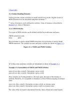
Two types of MOS switches can be defined with the keywords nmos and pmos.
//MOS switch keywords
nmos pmos
Keyword nmos is used to model NMOS transistors; keyword pmos is used to model
PMOS transistors. The symbols for nmos and pmos switches are shown in Figure 11-1
.
Figure 11-1. NMOS and PMOS Switches
In Verilog, nmos and pmos switches are instantiated as shown in Example 11-1
.
Example 11-1 Instantiation of NMOS and PMOS Switches
nmos n1(out, data, control); //instantiate a nmos switch
pmos p1(out, data, control); //instantiate a pmos switch
Since switches are Verilog primitives, like logic gates, the name of the instance is
optional. Therefore, it is acceptable to instantiate a switch without assigning an instance
name.
nmos (out, data, control); //instantiate an nmos switch; no instance name
pmos (out, data, control); //instantiate a pmos switch; no instance name
The value of the out signal is determined from the values of data and control signals.
Logic tables for out are shown in Table 11-1. Some combinations of data and control
signals cause the gates to output to either a 1 or 0, or to an z value without a preference
for either value. The symbol L stands for 0 or z; H stands for 1 or z.
Table 11-1. Logic Tables for NMOS and PMOS
Thus, the nmos switch conducts when its control signal is 1. If the control signal is 0, the
output assumes a high impedance value. Similarly, a pmos switch conducts if the control
signal is 0.
11.1.2 CMOS Switches
CMOS switches are declared with the keyword cmos.
A cmos device can be modeled with a nmos and a pmos device. The symbol for a cmos
switch is shown in Figure 11-2
.
Figure 11-2. CMOS Switch
A cmos switch is instantiated as shown in Example 11-2
.
Example 11-2 Instantiation of CMOS Switch
cmos c1(out, data, ncontrol, pcontrol);//instantiate cmos gate.
or
cmos (out, data, ncontrol, pcontrol); //no instance name given.
The ncontrol and pcontrol are normally complements of each other. When the ncontrol
signal is 1 and pcontrol signal is 0, the switch conducts. If ncontrol signal is 0 and
pcontrol is 1, the output of the switch is high impedance value. The cmos gate is
essentially a combination of two gates: one nmos and one pmos. Thus the cmos
instantiation shown above is equivalent to the following:
nmos (out, data, ncontrol); //instantiate a nmos switch
pmos (out, data, pcontrol); //instantiate a pmos switch
Since a cmos switch is derived from nmos and pmos switches, it is possible to derive the
output value from Table 11-1
, given values of data, ncontrol, and pcontrol signals.
11.1.3 Bidirectional Switches
NMOS, PMOS and CMOS gates conduct from drain to source. It is important to have
devices that conduct in both directions. In such cases, signals on either side of the device
can be the driver signal. Bidirectional switches are provided for this purpose. Three
keywords are used to define bidirectional switches: tran, tranif0, and tranif1.
tran tranif0 tranif1
Symbols for these switches are shown in Figure 11-3
below.
Figure 11-3. Bidirectional Switches
The tran switch acts as a buffer between the two signals inout1 and inout2. Either inout1
or inout2 can be the driver signal. The tranif0 switch connects the two signals inout1 and
inout2 only if the control signal is logical 0. If the control signal is a logical 1, the
nondriver signal gets a high impedance value z. The driver signal retains value from its
driver. The tranif1 switch conducts if the control signal is a logical 1.
These switches are instantiated as shown in Example 11-3
.
Example 11-3 Instantiation of Bidirectional Switches
tran t1(inout1, inout2); //instance name t1 is optional
tranif0 (inout1, inout2, control); //instance name is not specified
tranif1 (inout1, inout2, control); //instance name is not specified
Bidirectional switches are typically used to provide isolation between buses or signals.
11.1.4 Power and Ground
The power (Vdd, logic 1) and Ground (Vss, logic 0) sources are needed when transistor-
level circuits are designed. Power and ground sources are defined with keywords supply1
and supply0.
Sources of type supply1 are equivalent to Vdd in circuits and place a logical 1 on a net.
Sources of the type supply0 are equivalent to ground or Vss and place a logical 0 on a
net. Both supply1 and supply0 place logical 1 and 0 continuously on nets throughout the
simulation.
Sources supply1 and supply0 are shown below.
supply1 vdd;
supply0 gnd;
assign a = vdd; //Connect a to vdd
assign b = gnd; //Connect b to gnd
11.1.5 Resistive Switches
MOS, CMOS, and bidirectional switches discussed before can be modeled as
corresponding resistive devices. Resistive switches have higher source-to-drain
impedance than regular switches and reduce the strength of signals passing through them.
Resistive switches are declared with keywords that have an "r" prefixed to the
corresponding keyword for the regular switch. Resistive switches have the same syntax
as regular switches.
rnmos rpmos //resistive nmos and pmos switches
rcmos //resistive cmos switch
rtran rtranif0 rtranif1 //resistive bidirectional switches.
There are two main differences between regular switches and resistive switches: their
source-to-drain impedances and the way they pass signal strengths. Refer to Appendix A
,
Strength Modeling and Advanced Net Definitions, for strength levels in Verilog.
•
Resistive devices have a high source-to-drain impedance. Regular switches have a
low source-to-drain impedance.
•
Resistive switches reduce signal strengths when signals pass through them. The
changes are shown below. Regular switches retain strength levels of signals from
input to out
put. The exception is that if the input is of strength supply, the output is
of strong strength. Table 11-2
shows the strength reduction due to resistive
switches.
Table 11-2. Strength Reduction by Resistive Switches
Input Strength Output Strength
supply pull
strong pull
pull weak
weak medium
large medium
medium small
small small
high high
11.1.6 Delay Specification on Switches
MOS and CMOS switches
Delays can be specified for signals that pass through these switch-level elements. Delays
are optional and appear immediately after the keyword for the switch. Delay specification
is similar to that discussed in Section 5.2.1
, Rise, Fall, and Turn-off Delays. Zero, one,
two, or three delays can be specified for switches according to Table 11-3
.
Table 11-3. Delay Specification on MOS and CMOS Switches
Switch Element Delay Specification Examples