Tài liệu MEMS Mechanical Sensors ppt
Bạn đang xem bản rút gọn của tài liệu. Xem và tải ngay bản đầy đủ của tài liệu tại đây (4.07 MB, 281 trang )
MEMS Mechanical Sensors
For a listing of recent titles in the Artech House
Microelectromechanical Systems (MEMS) Series, turn to the back of this book.
MEMS Mechanical Sensors
Stephen Beeby
Graham Ensell
Michael Kraft
Neil White
Artech House, Inc.
Boston • London
www.artechhouse.com
Library of Congress Cataloging-in-Publication Data
A catalog record for this book is available from the U.S. Library of Congress.
British Library Cataloguing in Publication Data
Beeby, Stephen.
MEMS mechanical sensors.— (Artech House MEMS library)
1. Microelectricalmechanical systems—Design and construction 2. Transducers
I. Beeby, Stephen
621.3’81
ISBN 1-58053-536-4
Cover design by Igor Valdman
© 2004 ARTECH HOUSE, INC.
685 Canton Street
Norwood, MA 02062
All rights reserved. Printed and bound in the United States of America. No part of this book
may be reproduced or utilized in any form or by any means, electronic or mechanical, includ-
ing photocopying, recording, or by any information storage and retrieval system, without
permission in writing from the publisher.
All terms mentioned in this book that are known to be trademarks or service marks have
been appropriately capitalized. Artech House cannot attest to the accuracy of this informa-
tion. Use of a term in this book should not be regarded as affecting the validity of any trade-
mark or service mark.
International Standard Book Number: 1-58053-536-4
10987654321
Contents
Preface ix
CHAPTER 1
Introduction 1
1.1 Motivation for the Book 1
1.2 What Are MEMS? 2
1.3 Mechanical Transducers 3
1.4 Why Silicon? 4
1.5 For Whom Is This Book Intended? 5
References 5
CHAPTER 2
Materials and Fabrication Techniques 7
2.1 Introduction 7
2.2 Materials 7
2.2.1 Substrates 7
2.2.2 Additive Materials 11
2.3 Fabrication Techniques 11
2.3.1 Deposition 12
2.3.2 Lithography 17
2.3.3 Etching 21
2.3.4 Surface Micromachining 28
2.3.5 Wafer Bonding 29
2.3.6 Thick-Film Screen Printing 32
2.3.7 Electroplating 33
2.3.8 LIGA 34
2.3.9 Porous Silicon 35
2.3.10 Electrochemical Etch Stop 35
2.3.11 Focused Ion Beam Etching and Deposition 36
References 36
CHAPTER 3
MEMS Simulation and Design Tools 39
3.1 Introduction 39
3.2 Simulation and Design Tools 40
3.2.1 Behavioral Modeling Simulation Tools 40
3.2.2 Finite Element Simulation Tools 43
References 56
v
CHAPTER 4
Mechanical Sensor Packaging 57
4.1 Introduction 57
4.2 Standard IC Packages 58
4.2.1 Ceramic Packages 58
4.2.2 Plastic Packages 59
4.2.3 Metal Packages 59
4.3 Packaging Processes 59
4.3.1 Electrical Interconnects 60
4.3.2 Methods of Die Attachment 63
4.3.3 Sealing Techniques 65
4.4 MEMS Mechanical Sensor Packaging 66
4.4.1 Protection of the Sensor from Environmental Effects 67
4.4.2 Protecting the Environment from the Sensor 71
4.4.3 Mechanical Isolation of Sensor Chips 71
4.5 Conclusions 80
References 81
CHAPTER 5
Mechanical Transduction Techniques 85
5.1 Piezoresistivity 85
5.2 Piezoelectricity 89
5.3 Capacitive Techniques 92
5.4 Optical Techniques 94
5.4.1 Intensity 94
5.4.2 Phase 95
5.4.3 Wavelength 96
5.4.4 Spatial Position 96
5.4.5 Frequency 96
5.4.6 Polarization 97
5.5 Resonant Techniques 97
5.5.1 Vibration Excitation and Detection Mechanisms 98
5.5.2 Resonator Design Characteristics 99
5.6 Actuation Techniques 104
5.6.1 Electrostatic 104
5.6.2 Piezoelectric 107
5.6.3 Thermal 107
5.6.4 Magnetic 109
5.7 Smart Sensors 109
References 112
CHAPTER 6
Pressure Sensors 113
6.1 Introduction 113
6.2 Physics of Pressure Sensing 114
6.2.1 Pressure Sensor Specifications 117
6.2.2 Dynamic Pressure Sensing 120
vi Contents
6.2.3 Pressure Sensor Types 121
6.3 Traditional Pressure Sensors 121
6.3.1 Manometer 121
6.3.2 Aneroid Barometers 122
6.3.3 Bourdon Tube 122
6.3.4 Vacuum Sensors 123
6.4 Diaphragm-Based Pressure Sensors 123
6.4.1 Analysis of Small Deflection Diaphragm 125
6.4.2 Medium Deflection Diaphragm Analysis 127
6.4.3 Membrane Analysis 127
6.4.4 Bossed Diaphragm Analysis 128
6.4.5 Corrugated Diaphragms 129
6.4.6 Traditional Diaphragm Transduction Mechanisms 129
6.5 MEMS Technology Pressure Sensors 130
6.5.1 Micromachined Silicon Diaphragms 130
6.5.2 Piezoresistive Pressure Sensors 132
6.5.3 Capacitive Pressure Sensors 137
6.5.4 Resonant Pressure Sensors 139
6.5.5 Other MEMS Pressure Sensing Techniques 142
6.6 Microphones 143
6.7 Conclusions 145
References 145
CHAPTER 7
Force and Torque Sensors 153
7.1 Introduction 153
7.2 Silicon-Based Devices 154
7.3 Resonant and SAW Devices 157
7.4 Optical Devices 159
7.5 Capacitive Devices 160
7.6 Magnetic Devices 162
7.7 Atomic Force Microscope and Scanning Probes 164
7.8 Tactile Sensors 166
7.9 Future Devices 168
References 168
CHAPTER 8
Inertial Sensors 173
8.1 Introduction 173
8.2 Micromachined Accelerometer 175
8.2.1 Principle of Operation 175
8.2.2 Research Prototype Micromachined Accelerometers 180
8.2.3 Commercial Micromachined Accelerometer 192
8.3 Micromachined Gyroscopes 195
8.3.1 Principle of Operation 195
8.3.2 Research Prototypes 199
8.3.3 Commercial Micromachined Gyroscopes 204
Contents vii
8.4 Future Inertial Micromachined Sensors 206
References 207
CHAPTER 9
Flow Sensors 213
9.1 Introduction to Microfluidics and Applications for
Micro Flow Sensors 214
9.2 Thermal Flow Sensors 217
9.2.1 Research Devices 219
9.2.2 Commercial Devices 225
9.3 Pressure Difference Flow Sensors 229
9.4 Force Transfer Flow Sensors 232
9.4.1 Drag Force 232
9.4.2 Lift Force 235
9.4.3 Coriolis Force 236
9.4.4 Static Turbine Flow Meter 238
9.5 Nonthermal Time of Flight Flow Sensors 239
9.5.1 Electrohydrodynamic 239
9.5.2 Electrochemical 240
9.6 Flow Sensor Based on the Faraday Principle 241
9.7 Flow Sensor Based on the Periodic Flapping Motion 242
9.8 Flow Imaging 243
9.9 Optical Flow Measurement 245
9.9.1 Fluid Velocity Measurement 245
9.9.2 Particle Detection and Counting 246
9.9.3 Multiphase Flow Detection 246
9.10 Turbulent Flow Studies 247
9.11 Conclusion 248
References 250
About the Authors 257
Index 259
viii Contents
Preface
The field of microelectromechanical systems (MEMS), particularly micromachined
mechanical transducers, has been expanding over recent years, and the production
costs of these devices continue to fall. Using materials, fabrication processes, and
design tools originally developed for the microelectronic circuits industry, new
types of microengineered device are evolving all the time—many offering numerous
advantages over their traditional counterparts. The electrical properties of silicon
have been well understood for many years, but it is the mechanical properties that
have been exploited in many examples of MEMS. This book may seem slightly
unusual in that it has four editors. However, since we all work together in this field
within the School of Electronics and Computer Science at the University of South
-
ampton, it seemed natural to work together on a project like this. MEMS are now
appearing as part of the syllabus for both undergraduate and postgraduate courses
at many universities, and we hope that this book will complement the teaching that
is taking place in this area.
The prime objective of this book is to give an overview of MEMS mechanical
transducers. In order to achieve this, we provide some background information on
the various fabrication techniques and materials that can be used to make such
devices. The costs associated with the fabrication of MEMS can be very expensive,
and it is therefore essential to ensure a successful outcome from any specific produc-
tion or development run. Of course, this cannot be guaranteed, but through the use
of appropriate design tools and commercial simulation packages, the chances of
failure can be minimized. Packaging is an area that is sometimes overlooked in text
-
books on MEMS, and we therefore chose to provide coverage of some of the meth
-
ods used to provide the interface between the device and the outside world. The
book also provides a background to some of the basic principles associated with
micromachined mechanical transducers. The majority of the text, however, is dedi
-
cated to specific examples of commercial and research devices, in addition to dis
-
cussing future possibilities.
Chapter 1 provides an introduction to MEMS and defines some of the com
-
monly used terms. It also discusses why silicon has become one of the key materials
for use in miniature mechanical transducers. Chapter 2 commences with a brief dis
-
cussion of silicon and other materials that are commonly used in MEMS. It then
goes on to describe many of the fabrication techniques and processes that are
employed to realize microengineered devices. Chapter 3 reviews some of the com
-
mercial design tools and simulation packages that are widely used by us and other
researchers/designers in this field. Please note that it is not our intention to provide
critical review here, but merely to indicate the various features and functionality
ix
offered by a selection of packages. Chapter 4 describes some of the techniques and
structures that can be used to package micromachined mechanical sensors. It also
discusses ways to minimize unwanted interactions between the device and its
packaging. Chapter 5 presents some of the fundamental principles of mechanical
transduction. This chapter is largely intended for readers who might not have a
background in mechanical engineering. The remaining four chapters of the book are
dedicated to describing specific mechanical microengineered devices including pres
-
sure sensors (Chapter 6), force and torque sensors (Chapter 7), inertial sensors
(Chapter 8), and flow sensors (Chapter 9). These devices use many of the principles
and techniques described in the earlier stages of the book.
Acknowledgments
We authors express our thanks to all the contributing authors of this book. They are
all either present or former colleagues with whom we have worked on a variety of
MEMS projects over the past decade or so.
Steve Beeby
Graham Ensell
Michael Kraft
Neil White
Southampton, United Kingdom
April 2004
x Preface
CHAPTER 1
Introduction
1.1 Motivation for the Book
As we move into the third millennium, the number of microsensors evident in every
-
day life continues to increase. From automotive manifold pressure and air bag sen
-
sors to biomedical analysis, the range and variety are vast. It is interesting to note
that pressure sensors and ink-jet nozzles currently account for more than two-thirds
of the overall microtransducer market share. Future predications indicate that the
mechanical microsensor market will continue to expand [1]. One of the main rea
-
sons for the growth of microsensors is that the enabling technologies are based on
those used within the integrated circuit (IC) industry. The production cost of a com
-
mercial pressure sensor, for example, is around 1 Euro, and this is largely because
the cost of producing ICs is inversely proportional to the volume produced. The
trend in IC technology since the 1960s has been for the number of transistors on a
chip to double every 18 months; this is referred to as Moore’s law. This has pro-
found implications for the electronic systems associated with microsensors. In addi-
tion to the reduction of size there is added functionality and also the possibility of
producing arrays of individual sensor elements on the same chip.
Another feature that has influenced the popularity trend of microsensors is that
many (but certainly not all) are based on silicon (Si). The electrical properties of sili-
con have been studied for many years and are well understood and thoroughly
documented. Silicon also possesses many desirable mechanical properties that make
it an excellent choice for many types of mechanical sensor.
Today there are many companies working in the field of microelectromechani
-
cal systems (MEMS). A quick search on the Internet in July 2003 revealed several
hundred in the United States, Europe, and the Far East, including multinational cor
-
porations such as TRW Novasensor, Analog Devices, Motorola, Honeywell, Senso
-
Nor, Melexis, Infineon, and Mitsubishi, as well as small start-up companies. There
are also many conferences dedicated to the subject. A selection of examples (but by
no means an exhaustive list) is given here:
•
Transducers—International Conference on Solid-State Sensors and Actuators
(held biennially and rotating location between Asia, North America, and
Europe);
•
Eurosensors (held annually in Europe);
•
IEEE Sensors Conference (first held in 2002, annually United States and
Canada);
•
Micro Mechanics Europe—MME (held annually in Europe);
1
•
IEEE International MEMS Conference (rotates annually between the United
States, Asia, and Europe);
•
Micro and Nano Engineering—MNE (held annually in Europe);
•
Japanese Sensor Symposium (held annually in Japan);
•
Micro Total Analysis Systems— µTAS (held annually in the United States,
Asia, Europe, and Canada);
•
SPIE hold many symposia on MEMS at worldwide locations.
In addition, there are several journals that cover the field of microsensors and
sensor technologies, including:
•
Sensors and Actuators (A-Physical, B-Chemical);
•
IEEE/ASME Journal of Microelectromechanical Systems (JMEMS);
•
Journal of Micromechanics and Microengineering;
•
Measurement, Science and Technology;
•
Nanotechnology;
•
Microelectronic Engineering;
•
Journal of Micromechatronics;
•
Smart Materials and Structures;
•
Journal of Microlithography, Microfabrication, and Microsystems;
•
IEEE Sensors Journal;
•
Sensors and Materials.
The major advancements in the field of microsensors have undoubtedly taken
place within the past 20 years, and there is good reason to consider these as a mod-
ern technology. From an historical point of view, the interested reader might wish to
refer to a paper titled “There’s Plenty of Room at the Bottom” [2]. This is based on a
seminar given in 1959 by the famous physicist Richard Feynman where he consid
-
ered issues such as the manipulation of matter on an atomic scale and the feasibility
of fabricating denser electronic circuits for computers. He also considered the issues
of building smaller and smaller tools that could make even smaller tools so that
eventually the individual atoms could be manipulated. The effects of gravity become
negligible while those of surface tension and Van der Waals forces do not. Feynman
even offered a prize (subsequently claimed in 1960) to the first person who could
make an electric motor 1/64 in
3
(about 0.4 mm
3
). These size limits turned out to be
slightly too large and the motor was actually made using conventional mechanical
engineering methods that did not require any new technological developments.
1.2 What Are MEMS?
MEMS means different things to different people. The acronym MEMS stands for
microelectromechanical systems and was coined in the United States in the late
1980s. Around the same time the Europeans were using the phrase microsystems
technology (MST). It could be argued that the former term refers to a physical entity,
2 Introduction
while the latter is a methodology. The word “system” is common to both, implying
that there is some form of interconnection and combination of components. As an
example, a microsystem might comprise the following:
•
A sensor that inputs information into the system;
•
An electronic circuit that conditions the sensor signal;
•
An actuator that responds to the electrical signals generated within the circuit.
Both the sensor and the actuator could be MEMS devices in their own right. For
the purpose of this book, MEMS is an appropriate term as it specifically relates to
mechanical (micro) devices and also includes wider areas such as chemical sensors,
microoptical systems, and microanalysis systems.
There is also a wide variety of usage of terms such as transducer, sensor, actua
-
tor, and detector. For the purpose of this text, we choose to adopt the definition pro
-
posed by Brignell and White [3], where sensors and actuators are two subsets of
transducers. Sensors input information into the system from the outside world, and
actuators output actions into the external world. Detectors are merely binary sen
-
sors. While these definitions do not specifically relate to energy conversion devices,
they are simple, unambiguous, and will suffice for this volume.
As we will see in the following, micromachined transducers are generally (but
not exclusively) those that have been designed and fabricated using tools and tech-
niques originating from the IC industry. In general, there are two methods for sili-
con micromachining: bulk and surface. The former is a subtractive process whereby
regions of the substrate are removed; while with the latter technique layers are built
up on the surface of the substrate in an additive manner.
1.3 Mechanical Transducers
The market for micromachined mechanical transducers has, in the past, had the
largest slice of the pie of the overall MEMS market. This is likely to be the case in the
immediate future as well. The main emphasis of this text is on mechanical sensors,
including pressure, force, acceleration, torque, inertial, and flow sensors. Various
types of actuation mechanism, relevant to MEMS, will also be addressed together
with examples of the fundamental techniques used for mechanical sensors. The
main methods of sensing mechanical measurands have been around for many years
and are therefore directly applicable to microsensors. There is, however, a signifi
-
cant effect that must be accounted for when considering mesoscale devices (i.e.,
those that fit into the palm of your hand) and microscale devices. This is, of course,
scaling. Some physical effects favor the typical dimensions of micromachined
devices while others do not. For example, as the linear dimensions of an object are
reduced, other parameters do not shrink in the same manner. Consider a simple
cube of material of a given density. If the length l is reduced by a factor of 10, the
volume (and hence mass) will be reduced by a factor of 1,000 (l
3
). There are many
other consequences of scaling that need to be considered for fluidic, chemical, mag
-
netic, electrostatic, and thermal systems [4]. For example, an interesting effect, sig
-
nificant for microelectrostatic actuators operating in air, is Paschen’s law. This
1.3 Mechanical Transducers 3
states that the voltage at which sparking occurs (the breakdown voltage) is depend
-
ent on the product of air pressure and the separation between the electrodes. As the
gap between two electrodes is reduced, a plot of breakdown voltage against the gap
separation and gas pressure product (Paschen curve) reveals a minimum in the char
-
acteristic, as shown in Figure 1.1. The consequence is that for air gaps of less than
several microns, the breakdown voltage increases.
1.4 Why Silicon?
Micromachining has been demonstrated in a variety of materials including glasses,
ceramics, polymers, metals, and various other alloys. Why, then, is silicon so
strongly associated with MEMS? The main reasons are given here:
•
Its wide use within the microelectronic integrated circuit industry;
•
Well understood and controllable electrical properties;
•
Availability of existing design tools;
•
Economical to produce single crystal substrates;
•
Vast knowledge of the material exists;
•
Its desirable mechanical properties.
The final point is, of course, particularly desirable for mechanical microsensors.
Single crystal silicon is elastic (up to its fracture point), is lighter than aluminum, and
has a modulus of elasticity similar to stainless steel. Its mechanical properties are
anisotropic and hence are dependent on the orientation to the crystal axis. Table 1.1
illustrates some of the main properties of silicon in relation to other materials. Typi-
cal values are given and variations in these figures may be found in the literature as
some of the listed properties are dependent upon the measurement conditions used
to determine the values. Stainless steel is used as a convenient reference as it is widely
used in the manufacture of traditional mechanical transducers. It must be noted,
however, that there are many different types of stainless steel exhibiting a broad
variation to those values listed here.
Silicon itself exists in three forms: crystalline, amorphous, and polycrystalline
(polysilicon). High purity, crystalline silicon substrates are readily available as
4 Introduction
The Paschen curve
Air
Breakdown voltage (V)
100
1,000
10,000
1 10 100 1,000 10,000
Gap separation x gas pressure (microns*atm)
Figure 1.1 A plot of breakdown voltage against electrode separation (in air at 1 atmosphere of
pressure).
circular wafers with typical diameters of 100 mm (4 inches), 150 mm (6 inches), 200
mm (8 inches), or 300 mm (12 inches) in a variety of thicknesses. Amorphous silicon
does not have a regular crystalline form and contains many defects. Its main use has
been in solar cells, photo-sensors, and liquid crystal displays. Both amorphous and
polysilicon can be deposited as thin-films, usually less than about 5 µm thickness.
Other materials that are often used within the MEMS fabrication process include
glasses, quartz, ceramics, silicon nitride and carbide, alloys of various metals, and a
variety of specialist materials that are used for very specific purposes.
1.5 For Whom Is This Book Intended?
This book is intended for graduate researchers who have taken a first degree in elec-
tronics, electrical engineering, or the physical sciences. It is also aimed at senior
undergraduate students (years three or four) who are studying one of these courses.
The main subject area of the text is that of mechanical microsensors, and in order to
assist the reader in this respect, we have covered some of the fundamental principles
of applied mechanics that might not have been covered in detail during some of
these courses. Those who have a background in mechanical engineering will find
that this book provides an overview of some of the main transducer microfabrica
-
tion techniques that can be used to make a variety of transducer systems. Overall, it
should become clear that there is a synergy between the electrical and mechanical
engineering disciplines, and those who work in the field of sensors and actuators
will have the joy of participating in one of the truly interdisciplinary fields in the
whole of science.
References
[1] Nexus MST market analysis, .
[2] Feynman, R. P., “There’s Plenty of Room at the Bottom,” Journal of Microelectromechani
-
cal Systems, Vol. 1, No. 1, 1992, pp. 60–66.
[3] Brignell, J. E., and N. M. White, Intelligent Sensor Systems, Bristol, England: IOP
Publishing, 1994.
[4] Judy, J. W., “Microelectromechanical Systems (MEMS): Fabrication, Design and Applica
-
tions,” Smart Materials and Structures, Vol. 10, 2001, pp. 1115–1134.
1.5 For Whom Is This Book Intended? 5
Table 1.1 Properties of Silicon and Selected Other Materials
Property Si {111} Stainless
Steel
Al Al
2
O
3
(96%)
SiO
2
Quartz
Young’s modulus (GPa) 190 200 70 303 73 107
Poisson’s ratio 0.22 0.3 0.33 0.21 0.17 0.16
Density (g/cm
3
) 2.3 8 2.7 3.8 2.3 2.6
Yield strength (GPa) 7 3.0 0.17 9 8.4 9
Thermal coefficient of
expansion (10/K)
2.3 16 24 6 0.55 0.55
Thermal conductivity at
300K (W/cm⋅K)
1.48 0.2 2.37 0.25 0.014 0.015
Melting temperature (
o
C) 1,414 1,500 660 2,000 1,700 1,600
.
CHAPTER 2
Materials and Fabrication Techniques
2.1 Introduction
MEMS devices and structures are fabricated using conventional integrated circuit
process techniques, such as lithography, deposition, and etching, together with a
broad range of specially developed micromachining techniques. Those techniques
borrowed from the integrated circuit processing industry are essentially two dimen
-
sional, and control over parameters in the third dimension is only achieved by stack
-
ing a series of two-dimensional layers on the workpiece, which is usually a silicon
wafer. There are practical and economic limits, however, to the number of layers
that can be managed in such a serial process, and therefore, the expansion of devices
into the third dimension is restricted. Micromachining techniques enable structures
to be extended further into the third dimension; however, it has to be understood
that these structures are simply either extruded two-dimensional shapes or are gov-
erned by the crystalline properties of the material. True three-dimensional process-
ing would allow any arbitrary curved surface to be formed, and this is clearly not
possible with the current equipment and techniques. An important aspect of MEMS
is to understand the limitations of the micromachining techniques currently avail-
able. Although the range of these techniques is continually being expanded, there
are some core techniques that have been part of the MEMS toolkit for many years.
This chapter deals mainly with these core techniques, but also with those process
techniques borrowed from integrated circuit manufacturing.
2.2 Materials
2.2.1 Substrates
2.2.1.1 Silicon
Just as silicon has dominated the integrated circuit industry, so too is it predominant
in MEMS. There are a number of reasons for this: (1) pure, cheap, and well-
characterized material readily available; (2) a large number and variety of mature,
easily accessible processing techniques; and (3) the potential for integration with
control and signal processing circuitry. In addition to these reasons, the mechanical
and physical properties of silicon give it a powerful advantage for its use in mechani
-
cal sensors, and therefore, this book deals mainly with devices fabricated in bulk
silicon and silicon on insulator (SOI).
Crystalline silicon has a diamond structure. This is a face-centered cubic lattice
with two atoms (one at the lattice point and one at the coordinates ¼, ¼, ¼
7
normalized to the unit cell) associated with each lattice point. The crystal structure
is shown in Figure 2.1. The crystal planes and directions are designated by Miller
indices, as shown in Figure 2.2. Any of the major coordinate axes of the cube can be
designated as a <100> direction, and planes perpendicular to these are designated
as {100} planes. The {111} planes are planes perpendicular to the <111> directions,
which are parallel to the diagonals of the cube. Bulk silicon from material manufac
-
turers is usually either {100} or {111} orientation, although other orientations can
be obtained from specialist suppliers. This orientation identifies the plane of the top
surface of the wafer. The wafers are cut at one edge to form a primary flat in a {110}
plane. A secondary flat is also cut on another edge to identify the wafer orientation
and doping type, which is either n- or p-type. The doping is done with impurities to
give a resistivity of between 0.001 and 10,000 Ωcm. For mainstream integrated cir
-
cuit processing wafers are typically of the order of 10 to 30 Ωcm corresponding to
an impurity level of ∼3 × 10
14
cm
–3
for n-type and ∼9 × 10
14
cm
–3
for p-type.
Table 2.1 shows some of the properties of crystalline silicon. It should be remem
-
bered that some of the properties are anisotropic, and therefore, the orientation of
the silicon needs to be taken into account in the design of any mechanical sensor.
For example, the piezoresistance coefficient of single crystal silicon depends on the
orientation of the resistor with respect to the crystal orientation; Young’s modulus
is orientation dependent; cracks initiated through mechanical loading will tend to
propagate along certain crystal planes.
In the last few years, SOI wafers have become available and are now being
employed in MEMS applications. As shown in Figure 2.3, there are a number of dis-
tinct types of SOI wafer, each of which has its own particular features. Separation by
ion implantation of oxygen (Simox) wafers are fabricated by implanting bulk silicon
wafers with high-energy oxygen ions, followed by anneal at 1,300°C. This process
forms a buried oxide (BOX) layer at a fixed depth below the surface, leaving a
single-crystalline silicon layer (SOI layer) on the top surface. Although the SOI layer
8 Materials and Fabrication Techniques
Figure 2.1 Unit cell of silicon. The crystalline structure is face-centered cubic with two silicon
atoms associated with each lattice point. The dark atoms are on the lattice points and the gray
atoms are at (¼ ¼ ¼), (¼ ¾ ¾), (¾ ¼ ¾), and (¾ ¾ ¼).
Figure 2.2 Diagram illustrating the important planes and directions in crystalline silicon.
can be thickened by epitaxy, the thicknesses of the SOI and BOX layers are limited
due to the range and distribution of the implanted ions. Typically, these are ~0.2
and ∼0.1 µm, respectively. Wafer bonding is an alternative technique for producing
thick layers of silicon on a buried oxide. Two wafers, at least one of which is cov-
ered with a thick oxide layer, are bonded together by van der Waals forces, and sub-
sequent annealing at ∼1,100°C causes a chemical reaction that strengthens the
bonded interface. One of the wafers is then thinned down by mechanical grinding,
and a final polish can produce SOI films 1 µm thick with a uniformity of 10% to
30%. The BOX layer can be between 0.5 and 4 µm thick. These wafers are some-
times referred to as bonded and etched SOI (BESOI) wafers. Both ion implantation
and wafer bonding are used in the production of UNIBOND SOI wafers. Starting
with two wafers, the silicon surface of one wafer is first oxidized to form what will
become the buried oxide layer of the SOI structure. An ion implantation step, using
2.2 Materials 9
Table 2.1 Selected Properties of Crystalline Silicon
Yield strength (10
9
Nm
–2
)7
Knoop hardness (kgmm
–2
) 850
Young’s modulus (GPa), (100) orientation 160
Poisson’s ratio, (100) orientation 0.28
Density (gcm
–3
) 2.33
Lattice constant (Å) 5.435
Thermal expansion coefficient (10
–6
K
–1
) 2.6
Thermal conductivity (Wm
–1
K
–1
) 157
Specific heat (Jg
–1
K
–1
) 0.7
Melting point (°C) 1,410
Energy gap (eV) 1.12
Dielectric constant 11.9
Dielectric strength (10
7
Vm
–1
)3
Electron mobility (cm
2
V
–1
s
–1
) 1,450
Hole mobility (cm
2
V
–1
s
–1
) 505
High energy O ion
implantation
+
Anneal at 1,300ºC
SIMOX wafers
Oxidized handle
wafer
Bonded to second
wafter and annealed
at 1,100ºC
Ground and polished
device layer
BESOI wafers
Oxidize wafer
High energy
H ion
implantation
+
Handle wafer
bonded on top
Cleave along
plane
of weakness
Anneal at 1,100ºC
and polish
UNIBOND SOI wafers
Figure 2.3 Different manufacturing processes for SOI wafers.
hydrogen ions, is then executed through the oxide layer by a standard high-current
ion implanter to form the Smart Cut layer. The implanted hydrogen ions alter the
crystallinity of the silicon, creating a plane of weakness in the wafer. After the wafers
are bonded together, the implanted wafer can be cleaved along this plane to leave a
thin layer of silicon on top of the oxide layer. The wafer is then annealed at 1,100°C
to strengthen the bond, and the surface of the silicon is polished to reduce the defect
level to a level approaching that of bulk silicon. The buried oxide layer is pinhole
free. SOI layers in the range from 0.1 to 1.5 µm and BOX layers from 200 nm to 3
µm can be fabricated by this method.
Other substrates, however, should not be ignored. Among those that have been
used in micromachining are glasses, quartz, ceramics, plastics, polymers, and met
-
als. Quartz and glass are often used in MEMS mechanical sensors; therefore, a short
description of these materials is given here.
2.2.1.2 Quartz and Glasses
Quartz is mined naturally but is more commonly produced synthetically in large,
long faceted crystals. It has a trigonal trapezohedral crystal structure and is similar
to silicon in that it can be etched anisotropically by selectively etching some of the
crystal planes in etchants such as ammonium bifluoride or hydrofluoric acid. Unlike
silicon, however, this has not been extensively used as an advantage but has been
identified more as a disadvantage due to the development of unwanted facets and
poor edge definition after etching. Since the fastest etch rate is along the z-axis [1],
most crystalline quartz is cut with the z-axis perpendicular to the plane of the wafer.
The property of quartz that makes it useful in MEMS mechanical sensors is that it is
piezoelectrical. Quartz has been used to fabricate resonators, gyroscopes, and accel-
erometers. Another form of quartz is fused quartz, but be careful not to confuse this
material with crystalline quartz, as fused quartz is used to denote the glassy noncrys-
talline, and, therefore, isotropic form better known as silica. It is tough and hard and
has a very low expansion coefficient.
Glass can be etched in hydrofluoric acid solutions and is often electrostatically
bonded to silicon to make more complicated structures. Both phosphosilicate
and borosilicate glasses can be used. One of the more favored glasses is Pyrex,
which is a borosilicate glass composition with a coefficient of thermal expansion of
3.25 × 10
–6
/°C, which is close to that of silicon, an essential property for structures
to be used in thermally unstable environments. Some of the properties of quartz and
Pyrex are shown in Table 2.2. The substrate is sometimes used purely as a
10 Materials and Fabrication Techniques
Table 2.2 Selected Properties of Quartz and Pyrex
Property Quartz Pyrex
Young’s modulus (GPa) 107 64
Poisson’s ratio, (100) orientation 0.16 0.20
Density (gcm
–3
) 2.65 2.33
Dielectric constant 3.75 4.6
Thermal expansion coefficient (10
–6
K
–1
) 0.55 3.25
Thermal conductivity (Wm
–1
K
–1
) 1.38 1.13
Specific heat (Jg
–1
K
–1
) 0.787 0.726
Refractive index 1.54 1.474
foundation on which a micromachined device is built, in which case the substrate
material may be unimportant and need only be compatible with the processing
equipment used. Both quartz and Pyrex can be obtained in forms suitable for proc
-
essing using standard silicon processing equipment. Sometimes, however, the
device is formed in the substrate itself, in which case the material properties
become important.
2.2.2 Additive Materials
The materials deposited on the substrates include all those associated with inte
-
grated circuit processing. These are either epitaxial, polycrystalline, or amorphous
silicon, silicon nitride, silicon dioxide, silicon oxynitride, or a variety of metals and
metallic compounds, such as Cu, W, Al, Ti, and TiN, deposited by chemical (CVD)
or physical vapor deposition (PVD) processes. Organic polymer resists with thick
-
nesses up to the order of a few micrometers are deposited by optical or electron
beam lithography.
Additional materials used in MEMS mechanical sensors are: ceramics (e.g., alu
-
mina, which can be sputtered or deposited by a sol-gel process); polymers, such as
polyimides and thick X-ray resists and photoresists; a host of other metals and
metallic compounds (e.g., Au, Ni, ZnO) deposited either by PVD, electroplating, or
CVD; and alloys (e.g., SnPb) deposited by cosputtering or electroplating. Some
alloys, such as TiNi, have a shape memory effect that causes the material to return
to a predetermined shape when heated. This is caused by atomic shuffling within the
material during phase transition. At low temperatures the phase is martensite,
which is ductile and can be easily deformed. By simply heating, the phase of the
deformed material changes to austenite and the deformation induced at low tem-
perature can be fully recovered. The transition temperature depends on the impurity
concentration, which can be controlled to give values between –100°C and 100°C.
Therefore, by repeated deformation and heating the shape memory alloy (SMA) can
be incorporated in a useful mechanical device. For micromechanical devices the
high power-to-weight ratio, large achievable strain, low voltage required for heat
-
ing, and large mean time between failure suggest that SMAs have the potential for
superior actuators. The maximum frequency of operation, however, is only of the
order of 100 Hz [2]. Diamond and silicon carbide deposited by CVD have some
potentially useful mechanical and thermal properties. Each has high wear resistance
and hardness, is chemically inert, and has excellent heat resistance. Neither has been
extensively explored for their use in MEMS sensors.
It is safe to say that, unless there is an issue of contamination or the sensors are
integrated with circuitry, it is possible to deposit almost any material on the sub
-
strate. The issues that are likely to need addressing, however, are how well does it
adhere to the substrate, are there any stresses in the deposited layer that may cause it
to deform, and can it be patterned and etched using lithographic techniques?
2.3 Fabrication Techniques
The fabrication techniques used in MEMS consist of the conventional tech
-
niques developed for integrated circuit processing and a variety of techniques
2.3 Fabrication Techniques 11
developed specifically for MEMS. The three essential elements in conventional
silicon processing are deposition, lithography, and etching. These are illustrated in
Figure 2.4. The common deposition processes, which include growth processes, are
oxidation, chemical vapor deposition, epitaxy, physical vapor deposition, diffu
-
sion, and ion implantation. The types of lithography used are either optical or elec
-
tron beam, and etching is done using either a wet or dry chemical etch process.
Many of these conventional techniques have been modified for MEMS purposes,
for example, the use of thick photoresists, grayscale lithography, or deep reactive
ion etching. Other processes and techniques not used in conventional integrated cir
-
cuit fabrication have been developed specifically for MEMS, and these include sur
-
face micromachining, wafer bonding, thick-film screen printing, electroplating,
porous silicon, LIGA (the German acronym for Lithographie, Galvansformung,
Abformung), and focused ion beam etching and deposition. For a more general ref
-
erence covering MEMS fabrication techniques, see the book by Kovaks [3].
2.3.1 Deposition
2.3.1.1 Thermal Growth
Silicon dioxide is grown on silicon wafers in wet or dry oxygen ambient. This is
done in a furnace at temperatures in the range from 750°C to 1,200°C. For oxides
grown at atmospheric pressure the thickness of the oxide can be as small as 1.5 nm
or as large as 2 µm. For each micron of silicon dioxide grown, 0.45 µm of silicon is
consumed and this generates an appreciable compressive stress at the interface.
Furthermore, there is a large difference between the thermal expansion coefficients
of silicon and silicon dioxide, which leaves the oxide in compression after cool-
ing from the growth temperature, adding to the intrinsic stress arising during
growth. Stress is, of course, an important issue for MEMS mechanical devices and
12 Materials and Fabrication Techniques
Spin on
resist
Etch
Exposure
to UV light
through
mask
Develop
Deposit
layer
Deposition
Lithography
Strip resist
Etching
Figure 2.4 Illustration of the deposition, lithography, and etch processes.
cannot be ignored. Thick oxide films can cause bowing of the underlying substrate.
Freestanding oxide membranes will buckle and warp, and thin oxides on silicon
cantilevers will make them curl.
2.3.1.2 Chemical Vapor Deposition
Solid films, such as silicon dioxide, silicon nitride, and amorphous or polycrystal
-
line silicon (polysilicon) can be deposited on the surface of a substrate by a CVD
process, the film being formed by the reaction of gaseous species at the surface. The
three most common types of CVD process are low-pressure CVD (LPCVD), plasma
enhanced CVD (PECVD)—in which radio frequency (RF) power is used to generate
a plasma to transfer energy to the reactant gases, and atmospheric pressure CVD
(APCVD). For LPCVD, the step coverage (conformality), uniformity, and the com
-
position and stress of the deposited layer are determined by the gases used and the
operating temperature and pressure. For PECVD, the layer properties are affected
additionally by the RF power density, frequency, and duty cycle at which the reactor
is operated; and for APCVD, in which the deposition is mass transport limited, the
design of the reactor is significant.
2.3.1.3 Polysilicon and Amorphous Silicon
Films deposited by LPCVD are used widely in the integrated circuit industry.
Amorphous silicon and polysilicon, in particular, are usually deposited by LPCVD
using silane. Although polysilicon can be deposited by PECVD, this is generally
only done where large deposited areas are required or for thin-film transistor liquid
crystal displays. The properties of LPCVD amorphous silicon and polysilicon lay-
ers depend on the partial pressure of silane in the reactor, the deposition pressure
and temperature, and, if doped in situ, on the gas used for doping. If doped silicon
is required, then diborane, phosphine, or arsine is included in the deposition
process. The deposition temperatures range from 570°C for amorphous silicon to
650°C for polysilicon with the silicon grain size increasing with temperature. The
final grain size for amorphous silicon is usually determined, however, by the tem
-
perature at which the film is annealed after deposition. For MEMS devices anneal
-
ing can also be used to control the stress in amorphous and polysilicon films. The
residual stress in as-deposited amorphous silicon and polysilicon films can be as
much as 400 MPa and be either tensile or compressive depending on the deposition
temperature. The transition from tensile to compressive stress is quite sharp and
depends also on other deposition parameters, making it difficult to control the
stress in the as-deposited film. The residual stress in polysilicon deposited at 615°C
can be reduced to –10 MPa (compressive) by annealing for 30 minutes at 1,100°C
in N
2
and that in amorphous silicon films deposited at 580°C is reduced to 10 MPa
(tensile) by annealing for 30 minutes at 1,000°C in N
2
. Perhaps more importantly,
the residual stress gradient in these films is also reduced to near zero. An alternative
method is to deposit alternating layers of amorphous silicon grown at 570°C and
polysilicon grown at 615°C [4]. The amorphous silicon is tensile and the polysili
-
con is compressive. By adjusting the thickness and distribution in a multilayer film,
it is possible to control both the stress and the stress gradient in an as-deposited
polysilicon layer.
2.3 Fabrication Techniques 13
2.3.1.4 Epitaxy
Epitaxial silicon can be grown by APCVD or LPCVD. The ranges of temperatures at
which this is done are 900°C to 1,250°C for APCVD and 700°C to 900°C for
LPCVD. Epitaxy can be used to deposit silicon layers with clearly defined doping
profiles that can be used as an etch stop, such as, for example, an electrochemical
etch stop. It can also be used to thicken the SOI layers on Simox or UNIBOND
wafers, for which the thickness of the original SOI layer is restricted by the manufac
-
turing process. The most useful property of epitaxial silicon for MEMS applications,
though, may be the fact that it can be grown selectively. Silicon dioxide or silicon
nitride on wafers prevents the growth of epitaxial silicon, and a layer of amorphous
silicon or polysilicon is normally deposited instead. However, this deposition
process can be suppressed by the addition of HCl to the reaction gases. The HCl pre
-
vents spurious nucleation and growth of silicon on the silicon dioxide or nitride. An
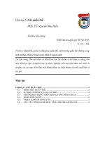
example of selective epitaxial growth is shown in Figure 2.5. This selective growth
can be used to form useful microengineered structures. Epitaxial silicon reactors can
also be used for depositing thick layers of polysilicon. Due to the growth time, poly
-
silicon deposited by LPCVD is often no more than a couple of microns thick,
whereas with the use of an epitaxial reactor, much thicker layers of more than 10 µm
can be deposited. This type of polysilicon is referred to as epipoly.
2.3.1.5 Silicon Nitride
Silicon nitride is commonly deposited by CVD by reacting silane or dichlorosilane
with ammonia. The film is in an amorphous phase and often contains a large
amount of hydrogen. LPCVD silicon nitride is an exceptionally good material for
masking against wet chemical etchants such as HF and hydroxide-based bulk silicon
anisotropic etchants. The deposition temperature, however, which is in the range
from 700°C to 850°C, prohibits its use on wafers with aluminum. Another limiting
factor is the large intrinsic tensile stress, which is of the order of 1 GPa. Layers
thicker than about 200 nm are likely to delaminate or crack, and freestanding
structures are susceptible to fracture. For MEMS applications, low-stress LPCVD
films can be deposited by increasing the ratio of silicon to nitrogen to produce silicon
14 Materials and Fabrication Techniques
5UM
P : 00003S : 0000020KV WD : 8MM8,84KX
Figure 2.5 Epitaxial silicon grown selectively between bars of oxide.