Tài liệu Các mạng UTMS và công nghệ truy cập vô tuyến P5 pptx
Bạn đang xem bản rút gọn của tài liệu. Xem và tải ngay bản đầy đủ của tài liệu tại đây (621.1 KB, 40 trang )
The UMTS Network and Radio Access Technology: Air Interface Techniques for Future Mobile Systems
Jonathan P. Castro
Copyright © 2001 John Wiley & Sons Ltd
Print ISBN 0-471-81375-3 Online ISBN 0-470-84172-9
T
HE
UTRA
1
T
RANSMISSION
S
YSTEM
5.1 UMTS S
PECTRUM
A
LLOCATION
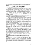
The UMTS frequency ranges are part of the world wide spectrum allocation for 3rd or
evolving 2nd generation systems. Figure 5.1 illustrates the representation of the spec-
trum from major regions (e.g. Europe, Japan, Korea, and USA).
'
Ã
'$
Ã
(
Ã
($
Ã
!
Ã
!$
Ã
!
Ã
! $
Ã
!!
Ã
V
T
6
Ã
Q8TÃ
@
V
S
P
Q
@
Ã
U99
Ã
9@8U
Ã
HTTÃÃVG
Ã
HTTÃÃ9G
Ã
U99
Ã
F
P
S
@
6
Ã
E
6
Q
6
I
Ã
0+]
Ã
BTH '
Ã
A99ÃÃVG
Ã
VHUTÃ
A99ÃÃ9G
Ã
VHUTÃ
DHU!Ã9G
Ã
DHU!ÃVGÃ
QCT
Ã
DHU!Ã9G
Ã
DHU!ÃVGÃ
DT($Ã9G
Ã
Q8T
Ã
9G
Ã
VG
Ã
VGvp
Ã
Figure 5.1 Spectrum allocation representation for 3G systems.
The distribution of the frequency bands from the allocated spectrum for the UTRA sys-
tem is covered next. We present the ranges for the FDD and the TDD in parallel in or-
der to unveil a complete view of the UMTS frequency assignment.
5.1.1 UTRA Frequency Bands
Table 5.1 summarizes the frequency bands for the TDD and FDD modes, as well as the
frequency distribution for the User Equipment (EU) and the Base Station (BS). Al-
though, in some cases the frequency ranges may be the same for both UE and BS, they
are noted separately for completeness.
Additional spectrum allocations in ITU region 2 are FFS, and deployment of UMTS in
existing and other frequency bands is not precluded. Furthermore, co-existence of TDD
and FDD in the same bands (now under study) may be possible.
_______
1
The UMTS Terrestrial Radio Access.
192 The UMTS Network and Radio Access Technology
Table 5.1 UTRA Frequency Bands in the MS and BS Side
FDD (MHz) TDD (MHz) up- and downlink
Case User equip-
ment
Base station User equip-
ment
Base station
(a) Uplink
(MS to BS) 1920–1980 1920–1980 1900–1920 1900–1920
Downlink
(BS to MS) 2110–2170 2110–2170 2010–2025 2010–2025
Region 2 – e.g. Europe
(b) Uplink
(MS to BS) 1850–1910 1850–1910 1850–1910 1850–1910
Downlink
(BS to MS) 1930–1990 1930–1990 1930–1990 1930–1990
(c) 1910–1930 1910–1930
5.2 R
ADIO
T
RANSMISSION AND
R
ECEPTION
A
SPECTS
After the allocation of the frequency ranges for the UTRA modes in the preceding sec-
tion, in the following we present the transceiver parameters from the technical
specifications, [1–4]. These parameters will set the necessary background to consider
equipment and network design, including traffic engineering issues.
5.2.1 Transmit to Receive (TX-RX) Frequency Separation
While the TDD mode does not need Frequency Separation (FS), the FDD mode does in
both the EU and the BS.
Table 5.2 UTRA TX-RX Frequency Separation
FDD TDD
User Equipment (UE) and Base Station (BS) UE and BS
1. Minimum value = 134.8 MHz
Maximum value = 245.2 MHz
All UE(s) shall support 190 MHz FS in case (a)
1
No TX-RX frequency separation is
required
2. All UE(s) shall support 80 MHz FS in case (b)
1
Each TDMA frame has 15 time slots
3. FDD Can support both fixed and variable
TX-RX FSs
4. Use of other TX-RX FSs in existing or other
frequency bands shall not be precluded
Each time slot can be allocated to
either transit (TX) or receive (RX)
1
When operating within spectrum allocations of cases (a) and (b) Table 5.1, respectively.
5.2.2 Channel Configuration
The channel spacing, raster and numbering arrangements aim to synchronize in both
FDD and TDD modes as well as keep certain compatibility with GSM, in order to
facilitate multi-mode system designs. This applies, e.g. to the raster distribution where
200 kHz corresponds to all (UE and BS in FDD and TDD modes). Table 5.3 summa-
rizes the specified channel configurations:
The UTRA Transmission System 193
Table 5.3 UTRA Channel Configurations
FDD (MHz) TDD (MHz)
Channel: UE and BS UE and BS
Spacing 5 MHz 5 MHz
Raster 200 kHz 200 kHz
UL N
u
=
5
(
1
F
uplink
MHz)
0.0 MHz F
uplink
3276.6 MHz
Number
DL N
d
= 5 (
1
F
downlink
MHz)
0.0 MHz F
downlink
3276.6
MHz
N
t
= 5 (F – MHz)
0.0 MHz F
3276.6 MHz
F is the carrier frequency in MHz
1
F
uplink
and F
downlink
are the uplink and downlink frequencies in MHz, respectively.
The nominal channel spacing (i.e. 5 MHz) can be adjusted to optimize performance
depending on the deployment scenarios; and the channel raster (i.e. 200 kHz) implies
the centre frequency which must be an integer multiple of 200 kHz.
In the case of the channel number, the carrier frequency is designated by the UTRA
Absolute Radio Frequency Channel Number (UARFCN), Table 5.3 shows those de-
fined in the IMT2000 band.
5.3 T
RANSMITTER
C
HARACTERISTICS
As in the UE or otherwise stated, we specify transmitter characteristics at the BS an-
tenna connector (test port A) with a full complement of transceivers for the configura-
tion in normal operating conditions. When using external apparatus (e.g. TX amplifiers,
diplexers, filters or a combination of such devices, requirements apply at the far end
antenna connector (port B).
5.3.1 Maximum Output Power
5.3.1.1 User Equipment (UE)
At this time detailed transmitter characteristics of the antenna connectors in the UE are not
available; thus, a reference UE with integral antenna and antenna gain of 0 dBi is as-
sumed. For the definition of the parameters to follow we use the UL reference measure-
ment channel (12.2 kbps) illustrated in Table 5.4, other references can be found in [1,2].
Table 5.4 UL Reference Measurement Channel Physical Parameters (12.2 kbps)
FDD TDD
Parameter Level Parameter Level
Information bit rate (kbps) 12.2 Information data rate 12.2 kbps
DPDCH (kbps) 60 RUs allocated 2 RU
DPCCH (kbps) 15 Mid-amble 512 chips
DPCCH/DPDCH (dB) –6 Interleaving 20 ms
TFCI On Power control 2 bit/user
Repetition (%) 23 TFCI 16 bit/user
Inband signalling DCCH 2 kbps
Puncturing level at code
rate 1/3 : DCH / DCCH
5%/0%
194 The UMTS Network and Radio Access Technology
About four UE power classes have been defined (Table 5.5). The tolerance of the
maximum output power is below the suggested level even when we would use multi-
code transmission mode in the FDD and TDD modes.
Other cases applying to the TDD mode from [2] are:
Maximum output power refers to the measure of power while averaged over the
useful part of transmit time slots with maximum power control settings.
In multi-code operation the maximum output power decreases by the difference of
the peak to average ratio between single and multi-code transmission.
UE using directive antennas for transmission, will have a class dependent limit
placed on the maximum Equivalent Isotropic Radiated Power (EIRP ).
Table 5.5 UE Power Classes
FDD TDD
Power Class Maximum output
power (dBm)
Tolerance (dB) Maximum output
power (dBm)
Tolerance (dB)
1 +33 +1/–3
2 +27 +1/–3 +24 +1/–3
3 +24 +1/–3 +21 +2/–2
4 +21 ±2
5.3.1.2 Base Station Output Power
In the TDD mode, BS output power, P
out
, represents the one carrier mean power deliv-
ered to a load with resistance equal to the nominal load impedance of the transmitter
during one slot. Likewise, BS rated output power, P
RAT
, indicates the manufacturer
declared mean power level per carrier over an active timeslot available at the antenna
connector [4].
In FDD or TDD BS maximum output power, P
max
, implies the mean power level per
carrier measured at the antenna connector in specified reference conditions. In normal
conditions, BS maximum output power remains within +2 dB and –2dB of the manufac-
turer’s rated output power. In extreme conditions, BS maximum output power remains
within +2.5 dB and –2.5 dB of the manufacturer’s rated output power.
5.3.2 Frequency Stability
Here frequency stability applies to both FDD and TDD modes. The required accuracy
of the UE modulated carrier frequency lies within
±
0.1 ppm when compared to the car-
rier frequency received from the BS. The signals have apparent errors as a result of BS
frequency error and Doppler shift; hence signals from the BS need averaging over suffi-
cient time.
The BS modulated carrier frequency is accurate to within ± 0.05 ppm for RF frequency
generation.
The UTRA Transmission System 195
5.3.3 Output Power Dynamics
5.3.3.1 User Equipment
In the FDD as well as TDD we use power control to limit interference. The Minimum
Transmit Output Power is better than –44 dBm measured with a Root-Raised Cosine
(RRC) filter having a roll-off factor
a = 0.22
and a bandwidth equal to the chip rate.
5.3.3.1.1 Open Loop Power Control
Open loop power control enables the UE transmitter to sets its output power to a spe-
cific value, where in normal conditions it has tolerance of ±9 dB and ±12 dB in extreme
conditions. We defined it as the average power in a time slot or ON power duration de-
pending on the availability. The two options are measured with a filter having a RRC
response with a roll off
a = 0.22
and a bandwidth equal to the chip rate.
5.3.3.1.2 Uplink Inner Loop Power Control
Through the uplink inner loop power control the UE transmitter adjusts its output power
according to one or more TPC command steps received in the downlink. The UE trans-
mitter will change the output power in step sizes of 1, 2 and 3 dB, depending on derived
D
TPC
or
D
RP-TPC
values in the slot immediately after the TPC_cmd. Tables 5.6 and 5.7
illustrate the transmitter power control range and average output power, respectively.
Table 5.6 Transmitter Power Control Range
TPC_cmd 1 dB step size 2 dB step size 3 dB step size
Lower Upper Lower Upper Lower Upper
+1 +0.5 +1.5 +1 +3 +1.5 +4.5
0 –0.5 +0.5 –0.5 +0.5 –0.5 +0.5
–1 –0.5 –1.5 –1 –3 –1.5 –4.5
We define the inner loop power as the relative power differences between averaged
power of original (reference) time slot and averaged power of the target time slot with-
out transient duration. The UE has minimum controlled output power with the power
control set to its minimum value. This applies to both inner loop and open loop power
control, where the minimum transmit power is better than –50 dBm [1]. They are meas-
ured with a filter that has a RRC filter response with a roll off
a = 0.22
and a bandwidth
equal to the chip rate.
Table 5.7 Transmitter Average Power Control Range
Transmitter power control range after 10
equal TPC_cmd groups
Transmitter power control range
after 7 equal TPC_cmd groups
1 dB step size 2 dB step size 3 dB step size
TPC_cmd
Lower Upper Lower Upper Lower Upper
+1 +8 +12 +16 +24 +16 +26
0 –1 +1 –1 +1 –1 +1
–1 –8 –12 –16 –24 –16 –26
0,0,0,0,+1 +6 +14 N/A N/A N/A N/A
0,0,0,0,–1 –6 –14 N/A N/A N/A N/A
196 The UMTS Network and Radio Access Technology
5.3.3.1.3 Uplink Power Control TDD
Through the uplink power control, the UE transmitter sets its output power taking into
account the measured downlink path loss, values determined by higher layer signalling
and filter response
a
. This power control has an initial error accuracy of less than
9 dB under normal conditions and
12dB under extreme conditions.
From [2] we define the power control differential accuracy as the error in the UE
transmitter power step, originating from a step in SIR
TARGET
when the parameter
a
= 0.
The step in SIR
TARGET
is rounded to the closest integer dB value. The error does not
exceed the values illustrated in Table 5.8.
Table 5.8 Transmitter Power Step Tolerance in Normal Conditions
1
DSIR
TARGET
(dB)
Transmitter power step
tolerance (dB)
DSIR
TARGET
1 0.5
1 < DSIR
TARGET
2 1
2 < DSIR
TARGET
3 1.5
3 < DSIR
TARGET
10 2
10 < DSIR
TARGET
20 4
20 < DSIR
TARGET
30 6
30 < DSIR
TARGET
9
1
1
For extreme conditions the value is
12.
5.3.3.2 Base Station
In FDD the transmitter uses a quality-based power control on both the uplink and
downlink to limit the interference level. In TDD the transmitter uses a quality-based
power control primarily to limit the interference level on the downlink.
Through inner loop power control in the downlink the FDD BS transmitter has the abil-
ity to adjust the transmitter output power of a code channel in accordance with the cor-
responding TPC symbols received in the uplink. In the TDD inner loop control is based
on SIR measurements at the UE receiver and the corresponding TPC commands are
generated by the UE, although the latte may or does also apply to the FDD.
5.3.3.2.1 Power control steps
The power control step change executes stepwise variation in the DL transmitter output
power of a code channel in response to a corresponding power control command. The
aggregated output power change represents the required total change in the DL trans-
mitter output power of a code channel while reacting to multiple consecutive power
control commands corresponding to that code channel. The BS transmitter will have the
capability of setting the inner loop output power with a step size of 1 dB mandatory and
0.5 dB optional [3]. The power control step and the aggregated output power change
due to inner loop power control shall be within the range illustrated in Table 5.9.
The UTRA Transmission System 197
In TDD, power control steps change the DL transmitter output power in response to a
TPC message from the UE in steps of 1, 2, and 3 dB. The tolerance of the transmitter
output power and the greatest average rate of change in mean power due to the power
control step will remain within the range illustrated in Table 5.10.
Table 5.9 FDD Transmitter Power Control Steps and Aggregated Output Power Change Range
Power control commands in the
down link
Transmitter power control step range
1 dB step size 0.5 dB step size
Lower Upper Lower Upper
Up (TPC command “1”) +0.5 +1.5 +0.25 +0.75
Down (TPC command “0”) –0.5 –1.5 –0.25 –0.75
Transmitter aggregated output power change range after 10
consecutive equal commands (up or down)
1 dB step size 0.5dB step size
Lower Upper Lower Upper
Up (TPC command “1”) +8 +12 +4 +6
Down (TPC command “0”) –8 –12 –4 –6
Table 5.10 TDD Power Control Step Size Tolerance
Range of average rate of change in mean power per 10 steps Step size Tolerance
Minimum Maximum
1dB
0.5dB
8dB
12dB
2dB
0.75dB
16dB
24dB
3dB
1dB
24dB
36dB
5.3.3.2.2 Power Control Dynamic Range and Primary CPICH–CCPCH Power
We refer to the difference between the maximum and the minimum transmit output
power of a code channel for a specified reference condition as the power control dy-
namic range. This range in the downlink (DL) has a maximum power
BS maximum
output power of –3 dB or greater, and minimum power
BS maximum output power
of –28 dB or less.
By total power dynamic range we mean the difference between the maximum and the
minimum total transmit output power for a specified reference condition. In this case,
the upper limit of the dynamic range is the BS maximum output power and the lower
limit the lowest minimum power from the BS when no traffic channels are activated.
The DL total power dynamic range is 18 dB or greater [3].
We call Primary CPICH power to the transmission power of the common pilot channel
averaged over one frame and indicated in a BCH. This power is within
2.1 dB of the
value indicated by a signalling message [3].
198 The UMTS Network and Radio Access Technology
In TDD, the power control dynamic range, i.e. the difference between the maximum
and the minimum transmit output power for a specified reference condition has a DL
minimum requirement of 30 dB. The minimum transmit power, i.e. the minimum con-
trolled BS output power with the power control setting set to a minimum value, has DL
maximum output power of –30 dB. The primary CCPCH power is averaged over the
transmit time slot and signalled over the BCH. The error between the BCH-broadcast
value of the primary CCPCH power and the primary CCPCH power averaged over the
time slot does not exceed the values illustrated in Table 5.11. The error is a function of
the total power averaged over the timeslot, P
out
, and the manufacturer’s rated output
power, P
RAT
[4].
Table 5.11 Errors Between Primary CCPCH Power and the Broadcast Value (TDD)
Total power in slot (dB) PCCPCH power tolerance (dB)
P
RAT
– 3 < P
out
P
RAT
+ 2 2.5
P
RAT
– 6 < P
out
P
RAT
– 3 3.5
P
RAT
– 13 < P
out
P
RAT
– 6 5
5.3.4 Out-of-Synchronization Output Power Handling
The UE monitors the DPCCH quality to detect L1 signal loss. The thresholds Q
out
and Q
in
specify at what DPCCH quality levels the UE shall shut its power off and
when it may turn its transmitter on, respectively. The thresholds are not defined ex-
plicitly, but are defined by the conditions under which the UE shuts its transmitter
off and turns it on.
Ã
9Q88Cf@pDÃbq7dÃ
6Ã Ã7Ã Ã8Ã ÃÃ9Ã @Ã
UvrÃbdÃ
b %%dÃ
b!!dÃ
b!'dÃ
b!#dÃ
b 'dÃ
V@ÃuÃrÃssÃ
V@ÃhÃÃrÃÃ
$Ã
U
ss
Ã
$Ã
R
RXW
Ã
R
LQ
Ã
$Ã
b#%d
U99Ã
b d
U99Ã
b !d
U99Ã
b%d
U99Ã
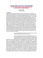
Figure 5.2 UE out-of-synch handling. Q
out
and Q
in
thresholds are for reference only [1].
Figure 5.2 illustrates the DPCH power level and the shutting off and on, where the re-
quirements for the UE from Refs. [1,2] are that:
The UTRA Transmission System 199
The UE shall not shut its transmitter off before point B.
The UE shall shut its transmitter off before point C, which is T
off
= [200] ms after
point B.
The UE shall not turn its transmitter on between points C and E.
The UE may turn its transmitter on after point E.
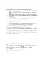
5.3.5 Transmit ON/OFF Power
Transmit OFF power state occurs when the UE does not transmit, except during UL
DTX mode (see Figure 5.3). We define this parameter as the maximum output transmit
power within the channel bandwidth when the transmitter is OFF. The requirement for
transmit OFF power shall be better than –56 dBm for FDD and –65 dBm for TDD, de-
fined as an averaged power within at least one time slot duration measured with a RRC
filter response having a roll off factor
a = 0.22
and a bandwidth equal to the chip rate.
8S/LQN
'3'&+
8S/LQN
'3&&+
6rhtrÃPIÃQr
Hvv
ÃÃQr
PAAÃQr
$Ã
$Ã
(%Ãpuv
UhvvÃrvq
PAAÃQr
(%puv
$Ãpuv
$Ãq7
7''
)''
6rhtrÃPIÃQr
Figure 5.3 Transmit ON/OFF template.
The time mask for transmit ON/OFF defines the UE ramping time allowed between
transmit OFF power and transmit ON power. This scenario may include the RACH,
CPCH or UL slotted mode. We define ON power as one of the following cases [1]:
first preamble of RACH: open loop accuracy;
during preamble ramping of the RACH and compressed mode: accuracy depending
on size of the power step;
power step to maximum power: maximum power accuracy.
Specifications in Ref. [1] describes power control events in Transport Format Combina-
tion (TFC ) and compressed modes.
200 The UMTS Network and Radio Access Technology
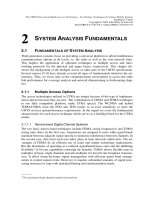
5.3.5.1 BS Transmit OFF Power (TDD)
When the BS does not transmit, it remains in transmit off power state, which we defined
as the maximum output transmit power within the channel bandwidth when the trans-
mitter states OFF. Its required level shall be better than –79 dBm measured with a RRC
filter response having a roll off
a
= 0.22 and a bandwidth equal to the chip rate.
The time mask transmit ON/OFF defines the ramping time allowed for the BS between
transmit OFF power and transmit ON power. The transmit power level vs. time meets
the mask illustrated in Figure 5.4.
%Ãpuv &%Ãpuv7ÃvuÃthqrvq
PAAÃQr
6rhtrÃPIÃQr
Figure 5.4 BS Transmit ON/OFF template (TDD).
5.3.6 Output RF Spectrum Emissions
5.3.6.1 Occupied Bandwidth and Out of Band Emission
Occupied bandwidth implies a measure of the bandwidth containing 99% of the total
integrated power of the transmitted spectrum, centred on the assigned channel fre-
quency. In the TDD as well as FDD, the occupied channel bandwidth shall be less than
5 MHz based on a chip rate of 3.84 Mcps.
Out of band emissions are unwanted emissions immediately outside the nominal chan-
nel originating from the imperfect modulation process and non-linearity in the transmit-
ter but excluding spurious emissions. A Spectrum emission mask and adjacent channel
leakage power ratio specify out of band emission limits.
5.3.6.2 Spectrum Emission Mask
The UE spectrum emission mask applies to frequencies that are between 2.5 MHz and
12.5 MHz away from the UE carrier frequency centre. The out of channel emission is
specified relative to the UE output power measured in a 3.84 MHz bandwidth. Table
5.12 illustrates UE power emission values, which shall not exceed specified levels.
The UTRA Transmission System 201
Table 5.12 Spectrum Emission Mask Requirement
Frequency offset from
carrier Df (MHz)
Minimum requirement
(dBc)
Measurement
bandwidth (MHz)
2.5–3.5 –35–15 (Df – 2.5) 30 kHz
3.5–7.5 –35–1 (Df – 3.5) 1
7.5–8.5 –39–10 (Df – 7.5) 1
8.5–12.5 –49 1
The first and last measurement position with a 30 kHz filter is 2.515 MHz and 3.485 MHz.
The first and last measurement position with a 1 MHz filter is 4 MHz and 12 MHz.
The lower limit shall be –50 dBm/3.84 MHz or which ever is higher.
The BS spectrum emission mask illustrated in Figure 5.5 and outlined in Table 5.13
may be mandatory in some regions and may not apply to others. Where it applies, BS
transmitting on a single RF carrier and configured according to the manufacturer’s
specification shall meet specified requirements. The mask basically applies to the FDD
and TDD.
!$ !& "$
$
ArrpÃrhhvÃDsÃsÃurÃphvrÃbHCd
Q
r
Ã
q
r
v
Ã
v
Ã
"
x
C
Ã
b
q
7
d
DI
PD[
!
!$
"
"$
#
Q
r
Ã
q
r
v
Ã
v
Ã
Ã
H
C
Ã
b
q
7
d
$
$
!
!$
&$
QÃ2Ã"(Ãq7
QÃ2Ã"(Ãq7
QÃ2Ã#"Ãq7
QÃ2Ã#"Ãq7
QÃ2Ã" Ãq7
QÃ2Ã" Ãq7
Figure 5.5 BS spectrum emission mask [3].
For example, emissions for the appropriate BS maximum output power, in the fre-
quency range from
D
f = 2.5 MHz to f_offset
max
from the carrier frequency, shall not
exceed the maximum level specified in Table 5.13 [3–4], where:
D
f = separation between the carrier frequency and the nominal –3 dB point of the
measuring filter closest to the carrier frequency.
F_offset = separation between the carrier frequency and the centre of the measuring
filter.
f_offset
max
= 12.5 MHz or is the offset to the UMTS Tx band edge, whichever is
the greater.
202 The UMTS Network and Radio Access Technology
Table 5.13 BS Spectrum Emission Mask Values
Df of measure-
ment filter –3 dB
point (MHz)
Df of filter measurement at
centre frequency (MHz)
Maximum level (dBm) Measure-
ment
bandwidth
BS maximum output power P 43 dBm
2.5 Df < 2.7 2.515 Df < 2.715 –14 30 kHz
2.7 Df < 3.5 2.715 Df < 3.515 –14–15¼(Df – 2.715) 30 kHz
3.515 Df < 4.0 –26 30 kHz
3.5 Df 4.0 Df < Df
max
–13 1 MHz
BS maximum output power 39 P < 43 dBm
2.5 Df < 2.7 2.515 Df < 2.715 –14 30 kHz
2.7 Df < 3.5 2.715 Df < 3.515 –14–15¼(Df – 2.715) 30 kHz
* 3.515 Df < 4.0 –26 30 kHz
3.5 Df < 7.5 4.0 Df < 7.5 –13 1 MHz
7.5 Df 7.5 Df < Df
max
P – 56 1 MHz
BS maximum output power 31 P < 39 dBm
2.5 Df < 2.7 2.515 Df < 2.715 P – 53 30 kHz
2.7 Df < 3.5 2.715 Df < 3.515
P
–
53
–
15
¼
(
D
f
–
2.715)
30 kHz
* 3.515 Df < 4.0 –26 30 kHz
3.5 Df < 7.5 4.0 Df < 7.5 P – 52 1 MHz
7.5 Df 7.5 Df < Df
max
P – 56 1 MHz
BS maximum output power P < 31 dBm
2.5 Df < 2.7 2.515 Df < 2.715 –22 30 kHz
2.7 Df < 3.5 2.715 Df < 3.515 –22 – 15¼(Df – 2.715) 30 kHz
* 3.515 Df < 4.0 –26 30 kHz
3.5 Df < 7.5 4.0 Df < 7.5 –21 1 MHz
7.5 Df 7.5 Df < Df
max
–25 1 MHz
*
This frequency range ensures that the range of values of
D
f is continuous.
5.3.6.3 Adjacent Channel Leakage Power Ratio (ACLR)
The ratio of the transmitted power to the power measured in an adjacent channel corre-
sponds to the Adjacent Channel Leakage Power Ratio (ACLR). Both the transmitted
and the adjacent channel power measurements use a RRC filter response with roll-off
a
=0.22 and a bandwidth equal to the chip rate. If the adjacent channel power greater
than –50 dBm then the ACLR shall be higher than the value specified in Table 5.14 [1].
Table 5.14 UE ACLR
Power
class
Adjacent channel relative to
UE channel (MHz)
ACLR limit (dB)
3 5 33
3 10 43
4 5 33
4 10 43
The UTRA Transmission System 203
5.3.6.4 Spurious Emissions
Spurious emissions or unwanted transmitter effects result from harmonics emission,
parasitic emission, inter-modulation products and frequency conversion products, but
not from band emissions. The frequency boundary and the detailed transitions of the
limits between the requirement for out band emissions and spectrum emissions are
based on ITU-R Recommendations SM.329. These requirements illustrated in Table
5.15 apply only to frequencies which are greater than 12.5 MHz away from the UE car-
rier frequency centre [1].
Table 5.15 General spurious emissions requirements
Frequency bandwidth Resolution bandwidth
(kHz)
Minimum requirement
(dBm)
9 kHz f < 150 kHz 1 –36
150 kHz f < 30 MHz 10 –36
30 MHz f < 1000 MHz 100 –36
1 GHz f < 12.75 GHz 1 MHz –30
Measurements integer multiples of 200 kHz.
5.3.6.5 Transmit Modulation and Inter-modulation
The transmit modulation pulse has a RRC shaping filter with roll-off
a
=0.22 in the
frequency domain. The impulse response of the chip impulse filter RC
0
(t) is:
()
() ()
VLQ FRV
&&&
&&
WWW
777
5& W
WW
77
ËÛËÛ
p-a+a p+a
ÌÜÌÜ
ÍÝÍÝ
=
ËÛ
ËÛ
ÌÜ
p-a
ÌÜ
ÌÜ
ÍÝ
ÍÝ
where the roll-off factor
a
=0.22 and the chip duration is T = 1/chip rate
0.26042
m
.
5.3.6.5.1 Vector Magnitude and Peak Code Domain Error
The Error Vector Magnitude (EVM) indicates a measure of the difference between the
measured waveform and the theoretical modulated waveform (the error vector). A
square root of the mean error vector power to the mean reference signal power ratio
expressed as a % defines the EVM. One time slot corresponds to the measurement in-
terval of one power control group. The EVM is less or equal to 17.5% for the UE output
power parameter (
–20 dBm) operating at normal conditions in steps of 1 dB.
The code domain error results from projecting the error vector power onto the code
domain at the maximum spreading factor. We define the error vector for each power
code as the ratio to the mean power of the reference waveform expressed in dB, and the
peak code domain error as the maximum value for the code domain error. The meas-
urement interval is one power control group (time slot). The requirement for the peak
code domain error applies only to multi-code transmission, and it shall not exceed
204 The UMTS Network and Radio Access Technology
–15 dB at a spreading factor of 4 for the UE output power parameter having a value
(
–20 dBm) and operating at normal conditions [1].
5.3.6.5.2 Inter-modulation
By transmit Inter-modulation (IM) performance we meant the measure of transmitter
capability to inhibit signal generation in its non-linear elements in the presence of
wanted signal and an interfering signal arriving to the transmitter via the antenna. For
example, user equipment(s) transmitting in close vicinity of each other can produce
inter-modulation products, which can fall into the UE, or BS receive band as an un-
wanted interfering signal.
We define UE inter-modulation attenuation as the output power ratio of wanted signal
to the output power of inter-modulation product when an interfering CW signal adds
itself at a level below a wanted signal. Both the wanted signal power and the IM prod-
uct power measurements use a RRC filter response with roll-off
a
= 0.22 and a band-
width equal to the chip rate. Table 5.16 illustrates IM requirement when transmitting
with 5 MHz carrier spacing.
Table 5.16 Transmit Inter-modulation
Interference signal frequency offset (MHz) 5 10
Interference CW signal level (dBc) –40
Inter-modulation product (dBc) –31 –41
5.4 R
ECEIVER
C
HARACTERISTICS
We specify receiver characteristics at the UE antenna connector, and for UE(s) with an
integral antenna only, we assume a reference antenna with a gain of 0 dBi. Receiver
characteristics for UE(s) with multiple antennas/antenna connectors are FFS.
5.4.1 Diversity
We assume appropriate receiver structure using coherent reception in both channel im-
pulse response estimation and code tracking procedures. The UTRA/FDD includes
three types of diversity:
time diversity
channel coding and interleaving in both up- and downlink;
multi-path diversity
rake receiver or other appropriate receiver structure with
maximum combining;
antenna diversity
occurs with maximum ratio combining in the BS and option-
ally in the MS.
5.4.2 Reference and Maximum Sensitivity Levels
Reference sensitivity implies the minimum receiver input power measured at the an-
tenna port at which the Bit Error Ratio (BER) does not exceed a specific value, e.g.
The UTRA Transmission System 205
BER = 0.001, the DPCH_Ec has a level of –117 dBm/3.48 MHz, and the Î
or
a level of
–106.7 dBm/3.84 MHz.
For the maximum input level, also with BER not exceeding 0.001, Î
or
= –25 dBm/3.84
MHz, and DPCH_Ec/Î
or
= –19 dB.
In the TDD mode reference sensitivity levels for
Ê
DPCH_Ec/Î
or
and Î
or
are 0 dB and
–105 dBm/3.84 MHz, respectively, while the maximum sensitive level requirements are
–7 dB and –25 dBm/3.84 MHz.
5.4.3 Adjacent Channel Selectivity (ACS)
Adjacent Channel Selectivity (ACS) refers to the measure of a receiver’s ability to re-
ceive a W-CDMA signal at its assigned channel frequency in the presence of an adja-
cent channel signal at a given frequency offset from the centre frequency of the as-
signed channel. We define the ACS as the ratio of receive filter attenuation on the as-
signed channel frequency to the receive filter attenuation on the adjacent channel(s) [1].
The ACS shall be better than 33 dB in Power Class 2(TDD), 3 and 4 for the test pa-
rameters specified in Table 5.17, where the BER shall not exceed 0.001.
Table 5.17 Test parameters for Adjacent Channel Selectivity
Parameter Unit Level
DPCH_Ec dBm/3.84 MHz –103
Î
or
dBm/3.84 MHz –92.7
I
oac
(modulated) dBm/3.84 MHz –52
F
uw
(offset) MHz 5
The (
Ê
DPCH_Ec/Î
or
)
TDD
has 0 dB as test parameter for the adjacent channel selectivity.
5.4.4 Blocking
The blocking characteristic indicates the measure of the receiver’s ability to receive a
wanted signal at its assigned channel frequency in the presence of an unwanted interfer-
ence on frequencies other than those of the spurious response or the adjacent channels.
The unwanted input signal shall not cause a degradation of the performance of the re-
ceiver beyond a specified limit, and the blocking performance shall apply at all frequen-
cies except those at which a spurious response occur.
The BER shall not exceed 0.001 for the parameters specified in Tables 7.6 and 7.7. For
Table 7.7 up to (24) exceptions are allowed for spurious response frequencies in each
assigned frequency channel when measured using a 1 MHz step size.
206 The UMTS Network and Radio Access Technology
Table 5.18 In-band Blocking FDD and TDD
Parameter Unit Offset Offset
Wanted signal
TDD
dBm/3.84 MHz <RefSens> + 3 dB <RefSens> + 3
dB
DPCH_Ec dBm/3.84 MHz –114 –114
Î
or
dBm/3.84 MHz –103.7 –103.7
I
blocking
(modulated)
applies to FDD and TDD
dBm/3.84 MHz –56 –44
F
uw
(offset) FDD and TDD MHz 10 15
Table 5.19 Out of Band Blocking FDD
Parameter Unit Band 1 Band 2 Band 3
DPCH_Ec dBm/3.84 MHz –114 –114 –114
Î
or
dBm/3.84 MHz –103.7 –103.7 –103.7
I
blocking
(CW) dBm –44 –30 –15
F
uw
MHz
2050<f <2095
2185<f <2230
2025 < f <2050
2230 < f <2255
1< f <2025
2255 < f < 12750
F
uw
MHz
1870<f <1915
2005<f <2050
1845 < f <1870
2050 < f <2075
1< f <1845
2075 < f < 12750
Table 5.20 Out of Band Blocking TDD
Parameter Unit Band 1 Band 2 Band 3
Wanted signal
dBm/
3.84 MHz
<RefSen> + 3 dB <RefSen> + 3 dB <RefSen> + 3 dB
Unwanted sig-
nal level (CW)
dBm –44 –30 –15
F
uw
MHz 1840 < f <1885
1935 < f <1995
2040 < f <2085
1815 < f <1840
2085 < f <2110
1< f <1815
2110< f <12750
F
uw
MHz 1790 < f < 1835
2005 < f < 2050
1765 < f < 1790
2050 < f < 2075
1 < f < 1765
2075 < f < 12750
F
uw
MHz 1850 < f < 1895
1945 < f < 1990
1825 < f < 1850
1990 < f < 2015
1 < f < 1825
2015 < f < 12750
The TDD out of band blocking differs from the FDD because they do not have the same
frequency range allocation.
5.4.5 Spurious Response
Through the spurious response, a receiver has the ability to receive a desired signal on
its assigned channel frequency, without exceeding a given degradation originating from
an undesired CW interfering signal. The latter occurs at any other frequency at which
the blocking limit is not met. Table 5.21 illustrates the spurious responses, where the
BER does not exceed 0.001.