Tài liệu Nano and Microelectromechanical Systems P3 doc
Bạn đang xem bản rút gọn của tài liệu. Xem và tải ngay bản đầy đủ của tài liệu tại đây (1.82 MB, 30 trang )
CHAPTER 3
STRUCTURAL DESIGN, MODELING, AND SIMULATION
3.1. NANO- AND MICROELECTROMECHANICAL SYSTEMS
3.1.1. Carbon Nanotubes and Nanodevices
Carbon nanotubes, discovered in 1991, are molecular structures which
consist of graphene cylinders closed at either end with caps containing
pentagonal rings. Carbon nanotubes are produced by vaporizing carbon
graphite with an electric arc under an inert atmosphere. The carbon
molecules organize a perfect network of hexagonal graphite rolled up onto
itself to form a hollow tube. Buckytubes are extremely strong and flexible
and can be single- or multi-walled. The standard arc-evaporation method
produces only multilayered tubes, and the single-layer uniform nanotubes
(constant diameter) were synthesis only a couple years ago. One can fill
nanotubes with any media, including biological molecules. The carbon
nanotubes can be conducting or insulating medium depending upon their
structure.
A single-walled carbon nanotube (one atom thick), which consists of
carbon molecules, is illustrated in Figure 3.1.1. The application of these
nanotubes, formed with a few carbon atoms in diameter, provides the
possibility to fabricate devices on an atomic and molecular scale. The
diameter of nanotube is 100000 times less that the diameter of the sawing
needle. The carbon nanotubes, which are much stronger than steel wire, are
the perfect conductor (better than silver), and have thermal conductivity
better than diamond. The carbon nanotubes, manufactured using the carbon
vapor technology, and carbon atoms bond together forming the pattern.
Single-wall carbon nanotubes are manufactured using laser vaporization, arc
technology, vapor growth, as well as other methods. Figure 3.1.2. illustrates
the carbon ring with six atoms. When such a sheet rolls itself into a tube so
that its edges join seamlessly together, a nanotube is formed.
Figure 3.1.1. Single-walled carbon nanotube
© 2001 by CRC Press LLC
Figure 3.1.2. Single carbon nanotube ring with six atoms
Carbon nanotubes, which allow one to implement the molecular wire
technology in nanoscale ICs, are used in NEMS and MEMS. Two slightly
displaced (twisted) nanotube molecules, joined end to end, act as the diode.
Molecular-scale transistors can be manufactured using different alignments.
There are strong relationships between the nanotube electromagnetic
properties and its diameter and degree of the molecule twist. In fact, the
electromagnetic properties of the carbon nanotubes depend on the molecule's
twist, and Figures 3.1.3 illustrate possible configurations. If the graphite
sheet forming the single-wall carbon nanotube is rolled up perfectly (all its
hexagons line up along the molecules axis), the nanotube is a perfect
conductor. If the graphite sheet rolls up at a twisted angle, the nanotube
exhibits the semiconductor properties. The carbon nanotubes, which are
much stronger than steel wire, can be added to the plastic to make the
conductive composite materials.
Figure 3.1.3. Carbon nanotubes
The vapor grown carbon nanotubes with N layers are illustrated in
Figure 3.1.4, and the industrially manufactured nanotubes have
∆ngstroms
diameter and length.
Figure 3.1.4. N-layer carbon nanotube
The carbon nanotubes can be organized as large-scale complex neural
networks to perform computing and data storage, sensing and actuation, etc.
The density of ICs designed and manufactured using the carbon nanotube
technology thousands time exceed the density of ICs developed using
convention silicon and silicon-carbide technologies.
© 2001 by CRC Press LLC
Metallic solids (conductor, for example copper, silver, and iron) consist
of metal atoms. These metallic solids usually have hexagonal, cubic, or body-
centered cubic close-packed structures (see Figure 3.1.5). Each atom has 8 or
12 adjacent atoms. The bonding is due to valence electrons that are
delocalized thought the entire solid. The mobility of electrons is examined to
study the conductivity properties.
(a) (b) (c)
Figure 3.1.5. Close packing of metal atoms: a) cubic packing;
b) hexagonal packing; c) body-centered cubic
More than two electrons can fit in an orbital. Furthermore, these two
electrons must have two opposite spin states (spin-up and spin-down).
Therefore, the spins are said to be paired. Two opposite directions in which
the electron spins (up +
2
1
and down –
2
1
) produce oppositely directed
magnetic fields. For an atom with two electrons, the spin may be either
parallel (S = 1) or opposed and thus cancel (S = 0). Because of spin pairing,
most molecules have no net magnetic field, and these molecules are called
diamagnetic (in the absence of the external magnetic field, the net magnetic
field produced by the magnetic fields of the orbiting electrons and the
magnetic fields produced by the electron spins is zero). The external
magnetic field will produce no torque on the diamagnetic atom as well as no
realignment of the dipole fields. Accurate quantitative analysis can be
performed using the quantum theory. Using the simplest atomic model, we
assume that a positive nucleus is surrounded by electrons which orbit in
various circular orbits (an electron on the orbit can be studied as a current
loop, and the direction of current is opposite to the direction of the electron
rotation). The torque tends to align the magnetic field, produced by the
orbiting electron, with the external magnetic field. The electron can have a
spin magnetic moment of
24
109
−
×±
A-m
2
. The plus and minus signs that
there are two possible electron alignments; in particular, aiding or opposing
to the external magnetic field. The atom has many electrons, and only the
spins of those electrons in shells which are not completely filed contribute to
the atom magnetic moment. The nuclear spin negligible contributes to the
atom moment. The magnetic properties of the media (diamagnetic,
paramagnetic, superparamagnetic, ferromagnetic, antiferromagnetic,
ferrimagnetic) result due to the combination of the listed atom moments
© 2001 by CRC Press LLC
Let us discuss the paramagnetic materials. The atom can have small
magnetic moment, however, the random orientation of the atoms results that
the net torque is zero. Thus, the media do not show the magnetic effect in the
absence the external magnetic field. As the external magnetic field is applied,
due to the atom moments, the atoms will align with the external field. If the
atom has large dipole moment (due to electron spin moments), the material is
called ferromagnetic. In antiferromagnetic materials, the net magnetic
moment is zero, and thus the ferromagnetic media are only slightly affected
by the external magnetic field.
Using carbon nanotubes, one can design electromechanical and
electromagnetic nanoswitches, which are illustrated in Figure 3.1.6.
Figure 3.1.6. Application of carbon nanotubes in nanoswitches
3.1.2. Microelectromechanical Systems and Microdevices
Different MEMS have been discussed, and it was emphasized that
MEMS can be used as actuators, sensors, and actuators-sensors. Due to the
limited torque and force densities, MEMS usually cannot develop high
torque and force, and large-scale cooperative MEMS are used, e.g.
multilayer configurations. In contrast, these characteristics (power, torque,
and force densities) are not critical in sensor applications. Therefore, MEMS
are widely used as sensors. Signal-level signals, measured by sensors, are fed
to analog or digital controllers, and sensor design, signal processing, and
interfacing are extremely important in engineering practice. Smart integrated
sensors are the sensors in which in addition to sensing the physical variable,
data acquisition, filtering, data storage, communication, interfacing, and
networking are embedded. Thus, while the primary component is the sensing
element (microstructure), multifunctional integration of sensors and ICs is
the current demand. High-performance accelerometers, manufactured by
Analog Devices using integrated microelectromechanical system technology
(iMEMS), are studied in this section. In addition, the application of smart
integrated sensors is discussed.
Nano-Antenna
nanotubeCarbon
Nanoswitch
hanicalElectromec
nanotubeCarbon
Nanoswitch
neticElectromag
Switching
OffOn
−
Nano-Antenna
© 2001 by CRC Press LLC
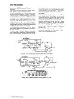
We study the dual-axis, surface-micromachined ADXL202 accelerometer
(manufactured on a single monolithic silicon chip) which combines highly
accurate acceleration sensing motion microstructure (proof mass) and signal
processing electronics (signal conditioning ICs). As documented in the Analog
Device Catalog data (which is attached), this accelerometer, which is
manufactured using the iMEMS technology, can measure dynamic positive and
negative acceleration (vibration) as well as static acceleration (force of gravity).
The functional block diagram of the ADXL202 accelerometer with two digital
outputs (ratio of pulse width to period is proportional to the acceleration) is
illustrated in Figure 3.1.7.
Figure 3.1.7. Functional block diagram of the ADXL202 accelerometer
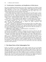
Polysilicon surface-micromachined sensor motion microstructure is
fabricated on the silicon wafer by depositing polysilicon on the sacrificial oxide
layer which is then etched away leaving the suspended proof mass (beam).
Polysilicon springs suspend this proof mass over the surface of the wafer. The
deflection of the proof mass is measured using the capacitance difference, see
Figure 3.1.8.
Demodulator
Demodulator
Y–Axis Sensor
X–Axis Sensor
Oscillator
Duty Cycle
Modulator
Output:
X–Axis
Output:
Y–Axis
© 2001 by CRC Press LLC
Figure 3.1.8. Accelerometer structure: proof mass, polysilicon springs, and
sensing elements (fixed outer plates and central movable
plates attached to the proof mass)
The proof mass (
m3.1
µ
,
m2
µ
thick) has movable plates which are
shown in Figure 3.1.8. The air capacitances
1
C and
2
C (capacitances between
the movable plate and two stationary outer plates) are functions of the
corresponding displacements
1
x and
2
x .
The parallel-plate capacitance is proportional to the overlapping area
between the plates (
m2m125
µ
µ
×
) and the displacement (up to
m3.1
µ
). In
particular, neglecting the fringing effects (nonuniform distribution near the
edges), the parallel-plate capacitance is
d
d
A
C
A
1
εε ==
,
where
ε
is the permittivity; A is the overlapping area; d is the displacement
between plates;
A
A
εε =
If the acceleration is zero, the capacitances
1
C and
2
C are equal
because
21
xx = (in ADXL202 accelerometer, m3.1
21
µ== xx ).
Thus, one has
Fixed Outer
Plates
m125
µ
Proof Mass:
Movable
Microstructure
m3.1
µ
Motion, x
Base (Substrate)
Polysilicon
Spring
Movable Plates
2
C
1
C
2
x
1
x
2
x
s
kSpring
2
1
,
s
kSpring
2
1
,
Polysilicon
Spring
Base (Substrate)
© 2001 by CRC Press LLC
21
CC = ,
where
1
1
1
x
C
A
ε= and
2
2
1
x
C
A
ε= .
The proof mass (movable microstructure) displacement x results due to
acceleration. If
0
≠
x , we have the following expressions for capacitances
xx
C
A
+
=
1
1
1
ε
and
xxxx
C
AA
−
=
−
=
12
2
11
εε
.
The capacitance difference is found to be
2
1
2
21
2
xx
x
CCC
A
−
=−=∆ ε
.
Measuring
C
∆
, one finds the displacement x by solving the following
nonlinear algebraic equation
02
2
1
2
=∆−−∆ CxxCx
A
ε .
For small displacements, neglecting the term
2
Cx∆ , one has
C
x
x
A
∆−≈
ε2
2
1
.
Hence, the displacement is proportional to the capacitance difference
C
∆
.
For an ideal spring, Hook’s law states that the spring exhibits a restoring
force F
s
which is proportional to the displacement x. Hence, we have the
following formula
F
s
= k
s
x,
where k
s
is the spring constant.
From Newton’s second law of motion, neglecting friction, one writes
xk
dt
xd
mma
s
==
2
2
.
Thus, the displacement due to the acceleration is
a
k
m
x
s
=
,
while the acceleration, as a function of the displacement, is given as
x
m
k
a
s
= .
Then, making use of the measured (calculated)
C
∆
, the acceleration is
found to be
C
m
xk
a
A
s
∆−=
ε2
2
1
.
Making use of Newton’s second law of motion, we have
© 2001 by CRC Press LLC
force spring
2
2
)(xf
dt
xd
mma
s
== ,
where
)(xf
s
is the spring restoring force which is a nonlinear function of the
displacement, and
3
3
2
21
)( xkxkxkxf
ssss
++= ; k
s1
, k
s2
and k
s3
are the
spring constants.
Therefore, the following nonlinear equation results
3
3
2
21
xkxkxkma
sss
++= .
Thus,
(
)
3
3
2
21
1
xkxkxk
m
a
sss
++= ,
where
C
x
x
A
∆−≈
ε2
2
1
.
This equation can be used to calculate the acceleration a using the
capacitance difference
C
∆
.
Two beams (proof masses which are motion microstructures) can be
placed orthogonally to measure the accelerations in the X and Y axis
(ADXL250), as well as the movable plates can be mounted along the sides of
the square beam (ADXL202). Figures 3.1.9 and 3.1.10 document the
ADXL202 and ADXL250 accelerometers.
© 2001 by CRC Press LLC
Figure 3.1.9. ADXL202 accelerometer: proof mass with fingers and ICs
(courtesy of Analog Devices)
© 2001 by CRC Press LLC
Figure 3.1.10.ADXL250 accelerometer: proof masses with fingers and ICs
(courtesy of Analog Devices)
Responding to acceleration, the proof mass moves due to the mass of the
movable microstructure (m) along X and Y axes relative to the stationary
member (accelerometer). The motion of the proof mass is constrained, and the
polysilicon springs hold the movable microstructure (beam). Assuming that the
polysilicon springs and the proof mass obey Hook’s and Newton’s laws, it was
shown that the acceleration is found using the following formula
© 2001 by CRC Press LLC
x
m
k
a
s
= .
The fixed outer plates are excited by two square wave 1 MHz signals of
equal magnitude that are 180 degrees out of phase from each other. When the
movable plates are centered between the fixed outer plates we have
21
xx = .
Thus, the capacitance difference
C
∆
and the output signal is zero. If the proof
mass (movable microstructure) is displaced due to the acceleration, we have
0
≠
∆
C . Thus, the capacitance imbalance, and the amplitude of the output
voltage is a function (proportional) to the displacement of the proof mass x.
Phase demodulation is used to determine the sign (positive or negative) of
acceleration. The ac signal is amplified by buffer amplifier and demodulated by
a synchronous synchronized demodulator. The output of the demodulator
drives the high-resolution duty cycle modulator. In particular, the filtered signal
is converted to a PWM signal by the 14-bit duty cycle modulator. The zero
acceleration produces 50% duty cycle. The PWM output fundamental period
can be set from 0.5 to 10ms.
There is a wide range of industrial systems where smart integrated sensors
are used. For example, accelerometers can be used for
1. active vibration control and diagnostics,
2. health and structural integrity monitoring,
3. internal navigation systems,
4. earthquake-actuated safety systems,
5. seismic instrumentation: monitoring and detection,
6. etc.
Current research activities in analysis, design, and optimization of
flexible structures (aircraft, missiles, manipulators and robots, spacecraft,
surface and underwater vehicles) are driven by requirements and standards
which must be guaranteed. The vibration, structural integrity, and structural
behavior are addressed and studied. For example, fundamental, applied, and
experimental research in aeroelasticity and structural dynamics are conducted
to obtain fundamental understanding of the basic phenomena involved in
flutter, force and control responses, vibration, and control. Through
optimization of aeroelastic characteristics as well as applying passive and
active vibration control, the designer minimizes vibration and noise, and
current research integrates development of aeroelastic models and
diagnostics to predict stalled/whirl flutter, force and control responses,
unsteady flight, aerodynamic flow, etc. Vibration control is a very
challenging problem because the designer must account complex interactive
physical phenomena (elastic theory, structural and continuum mechanics,
radiation and transduction, wave propagation, chaos, et cetera). Thus, it is
necessary to accurately measure the vibration, and the accelerometers, which
allow one to measure the acceleration in the micro-g range, are used. The
application of the MEMS-based accelerometers ensures small size, low cost,
© 2001 by CRC Press LLC
ruggedness, hermeticity, reliability, and flexible interfacing with
microcontrollers, microprocessors, and DSPs.
High-accuracy low-noise accelerometers can be used to measure the
velocity and position. This provides the back-up in the case of the GPS system
failures or in the dead reckoning applications (the initial coordinates and speed
are assumed to be known). Measuring the acceleration, the velocity and
position in the xy plane are found using integration. In particular,
∫
=
f
t
t
xx
dttatv
0
)()( ,
∫
=
f
t
t
yy
dttatv
0
)()( ,
∫
=
f
t
t
xx
dttvtx
0
)()( ,
∫
=
f
t
t
yy
dttvtx
0
)()( .
The Analog Devices data for iMEMS accelerometers
ADXL202/ADXL210 and ADXL150/ADXL250 are given below (courtesy of
Analog Devices).
It is important to emphasize that microgyroscope have been designed,
fabricated, and deployed using the similar technology as iMEMS
accelerometers. In particular, using the difference capacitance (between the
movable rotor and stationary stator plates), the angular acceleration is
measured. The butterfly-shaped polysilicon rotor suspended above the
substrate, and Figure 3.1.11 illustrates the microgyroscope.
Figure 3.1.11. Angular microgyroscope structure
Angular
displacement
Rotor:
Movable
Microstructure
Movable Plates
Stator: Stationary Base
Stationary Plates
© 2001 by CRC Press LLC
Microaccelerometer Mathematical Model
Using the experimental data (input-output dynamic behavior and Bode
plots), the mathematical model of microaccelerometers is obtained in the form
of ordinary differential equations, and the coefficients (accelerometer
parameters) are identified. The dominant microaccelerometer dynamics is
described by a system of six linear differential equations
,, CxyBuAx
dt
dx
=+=
where the matrices of coefficients are
[ ]
.
,,
27
27232014104
107.300000
0
0
0
0
0
1
010000
001000
000100
000010
000001
107.3109105.1102.4107.2106.2
×
×−×−×−×−×−×−
=
=
=
C
BA
The accelerometer output, which is the measured acceleration a, was
denoted as y, y = a. It is evident that the acceleration is a function of the state
variable x
6
. All other five states model the proof mass (motion microstructure)
and microICs (oscillator, demodulator, modulator, filter, et cetera) dynamics.
The eigenvalues are found to be
4353
108.8102.4,104.1109.5 ×±×−×±×− ii , .104103
33
×±×− i
This mathematical model of the microaccelerometer can be used in
systems analysis, diagnostics, and design of a wide variety of systems where
iMEMS are used.
© 2001 by CRC Press LLC
142
Chapter three: Structural design, modeling, and simulation
FEATURES
2-Axis Acceleration Sensor on a Single IC Chip
Measures Static Acceleration as Well as Dynamic
Acceleration
Duty Cycle Output with User Adjustable Period
Low Power <0.6 mA
Faster Response than Electrolytic, Mercury or Thermal
Tilt Sensors
Bandwidth Adjustment with a Single Capacitor Per Axis
5 m
g
Resolution at 60 Hz Bandwidth
+3 V to +5.25 V Single Supply Operation
1000
g
Shock Survival
APPLICATIONS
2-Axis Tilt Sensing
Computer Peripherals
Inertial Navigation
Seismic Monitoring
Vehicle Security Systems
Battery Powered Motion Sensing
GENERAL DESCRIPTION
The ADXL202/ADXL210 are low cost
,
low power
,
complete
2-axis accelerometers with a measurement range of either
±
2
g
/
±
10
g
. The ADXL202/ADXL210 can measure both dy-
namic acceleration (e.g.
,
vibration) and static acceleration (e.g.
,
gravity).
The outputs are digital signals whose duty cycles (ratio of pulse-
width to period) are proportional to the acceleration in each of
the 2 sensitive axes. These outputs may be measured directly
with a microprocessor counter
,
requiring no A/D converter or
glue logic. The output period is adjustable from 0.5 ms to 10 ms
via a single resistor (R
SET
). If a voltage output is desired
,
a
voltage output proportional to acceleration is available from the
X
FILT
and Y
FILT
pins
,
or may be reconstructed by filtering the
duty cycle outputs.
The bandwidth of the ADXL202/ADXL210 may be set from
0.01 Hz to 5 kHz via capacitors C
X
and C
Y
. The typical noise
floor is 500
µ
g
/ allowing signals below 5 m
g
to be resolved
for bandwidths below 60 Hz.
The ADXL202/ADXL210 is available in a hermetic 14-lead
Surface Mount CERPAK
,
specified over the 0°C to
+
70°C com-
mercial or
−
40°C to
+
85°C industrial temperature range.
i
MEM
S is a registered trademark of Analog Devices
,
Inc.
REV. B
Information fumishisd by Analog Devices is believed to be accurate
and reliable. However, no responsibility is assumed by Analog Devices
for its use, nor for any infringements of patents or other rights of third
parties which may result from its use. No license is granted by impli-
cation or otherwise under any patent or patent rights of Analog Devices.
One Technology Way, P.O. Box 9106, Norwood, MA 02062-9106, U.S.A.
Tel: 781/329-4700 World Wide Web Site:
Fax: 781/326-8703 © Analog Devices, Inc., 1999
Hz
FUNCTIONAL BLOCK DIAGRAM
ADXL202/ADXL210
Low Cost ±2
g
/±10
g
Dual Axis
i
MEM
S
®
Accelerometers
with Digital Output
© 2001 by CRC Press LLC
Chapter three: Structural design, modeling, and simulation
143
ADXL202/ADXL210–SPECIFICATIONS
(T
A
= T
MIN
to T
MAX
, T
A
= +25°C for J Grade only, V
DD
= +5 V,
R
SET
= 125 k
Ω
, Acceleration = 0
g
, unless otherwise noted)
ADXL202/JQC/AQC ADXL210/JQC/AQC
Parameter Conditions Min Typ Max Min Typ Max Units
SENSOR INPUT
Measurement Range
1
Nonlinearity
Alignment Error
2
Alignment Error
Transverse Sensitivity
3
Each Axis
Best Fit Straight Line
X Sensor to Y Sensor
±
1.5
±
2
0.2
±
1
±
0.01
±
2
±
8
±
10
0.2
±
1
±
0.01
±
2
g
% of FS
Degrees
Degrees
%
SENSITIVITY
Duty Cycle per
g
Sensitivity
,
Analog Output
Temperature Drift
4
Each Axis
T1/T2
@
+25°C
At Pins X
FILT
,
Y
FILT
∆
from +25°C
10 12.5
312
±
0.5
15 3.2 4.0
100
±
0.5
4.8 %/
g
mV/
g
% Rdg
ZERO
g
BIAS LEVEL
0
g
Duty Cycle
Initial Offset
0
g
Duty Cycle vs. Supply
0
g
Offset vs. Temperature
4
Each Axis
T1/T2
∆
from
+
25°C
25 50
±
2
1.0
2.0
75
4.0
42 50
±
2
1.0
2.0
58
4.0
%
g
%/V
m
g
/°C
NOISE PERFORMANCE
Noise Density
5
@
+
25°C 500 1000 500 1000
FREQUENCY RESPONSE
3 dB Bandwidth
3 dB Bandwidth
Sensor Resonant Frequency
Duty Cycle Output
At Pins X
FILT
,
Y
FILT
500
5
10
500
5
14
Hz
kHz
kHz
FILTER
R
FILT
Tolerance
Minimum Capacitance
32 k
Ω
Nominal
At X
FILT
,
Y
FILT
1000
±
15
1000
±
15 %
pF
SELF TEST
Duty Cycle Change Self-Test
“
0
”
to
“
1
”
10 10 %
DUTY CYCLE OUTPUT STAGE
F
SET
F
SET
Tolerance
Output High Voltage
Output Low Voltage
T2 Drift vs. Temperature
Rise/Fall Time
R
SET
=
125 k
Ω
I
=
25
µ
A
I
=
25
µ
A
0.7
35
200
1.3
200
0.7
35
200
1.3
200
kHz
mV
mV
ppm/°C
ns
POWER SUPPLY
Operating Voltage Range
Specified Performance
Quiescent Supply Current
Turn-On Time
6
To 99%
3.0
4.75
0.6
5.25
5.25
1.0
2.7
4.75
0.6
5.25
5.25
1.0
V
V
mA
ms
TEMPERATURE RANGE
Operating Range
Specified Performance
JQC
AQC
0
−
40
+
70
+
85
0
−
40
+
70
+
85
°C
°C
NOTES
1
For all combination of offset no sensitivity variation.
2
Alignment error is specified as the angle between the true and indicated axis of sensitivity.
3
Transverse sensitivity is the algebraic non of the alignment and the inherent sensitivity errors.
4
Specification refers to the maximum change in parameter from its initial at
+
25°C to its worst case value at T
MIN
T
MAX
.
5
Noose density is the average noise at any frequency in the bandwith of the part.
6
C
FILT
in
µ
F. Addition of filter capacitor will increase turn on time. Please see the Application section on power cycling.
All min and max specifications are guaranteed. Typical specifications are not tested or guaranteed.
Specifications subject to change without notice.
µg/Hz
µg/Hz()
125 M
Ω
/R
SET
125 M
Ω
/R
SET
V
S
−
200 mV
V
S
−
200 mV
160 C
FILT
+
0.3
160 C
FILT
+
0.3
© 2001 by CRC Press LLC
144
Chapter three: Structural design, modeling, and simulation
ADXL202/ADXL210
ABSOLUTE MAXIMUM RATINGS*
Acceleration (Any Axis
,
Unpowered for 0.5 ms) . . . . . 1000
g
Acceleration (Any Axis
,
Powered for 0.5 ms) . . . . . . . .500
g
+
V
S
. . . . . . . . . . . . . . . . . . . . . . . . . . . . . . . .
−
0.3 V to
+
7.0 V
Output Short Circuit Duration
(Any Pin to Common) . . . . . . . . . . . . . . . . . . . . . . . Indefinite
Operating Temperature . . . . . . . . . . . . . . . . .
−
55°C to
+
125°C
Storage Temperature. . . . . . . . . . . . . . . . . . .
−
65°C to
+
I 50°C
*Stresses above those listed under Absolute Maximum Ratings may cause perma-
nent damage to the device. This is a stress rating only
;
the functional operation of
the device at these or any other conditions above those indicated in the operational
sections of this specification is not implied. Exposure to absolute maximum rating
conditions for extended periods may affect device reliability.
Drops onto hard surfaces can cause shocks of greater than 1000
g
and exceed the absolute maximum rating of the device. Care
should be exercised in handling to avoid damage.
PIN FUNCTION DESCRIPTIONS
Pin Name Description
1 NC Not Connect
2 V
TP
Test Point
,
Do Not Connect
3 ST Self Test
4 COM Common
5 T2 Connect R
SET
to Set T2 Period
6 NC No Connect
7 COM Common
8 NC No Connect
9 Y
OUT
Y Axis Duty Cycle Output
10 X
OUT
X Axis Duty Cycle Output
11 Y
FILT
Connect Capacitor for Y Filter
12 X
FILT
Connect Capacitor for X Filter
13 V
DD
+
3 V to
+
5.25 V
,
Connect to 14
14 V
DD
+
3 V to
+
5.25 V
,
Connect to 13
PACKAGE CHARACTERISTICS
Package
θ
JA
θ
JC
Device Weight
14-Lead CERPAK 110°C/W 30°C/W 5 Grams
PIN CONFIGURATION
Figure 1 shows the response of the ADXL202 to the Earth
’
s
gravitational field. The output values shown are nominal. They
are presented to show the user what type of response to expect
from each of the output pins due to changes in orientation with
respect to the Earth. The ADXL210 reacts similarly with output
changes appropriate to its scale.
Figure 1. ADXL202/ADXL210 Nominal Response Due to
Gravity
ORDERING GUIDE
Model
g
Range
Temperature
Range
Package
Description
Package
Option
ADXL202JQC
±
2 0°C to
+
70°C 14-Lead CERPAK QC-14
ADXL202AQC
±
2
−
40°C to +85°C 14-Lead CERPAK QC-14
ADXL210JQC
±
10 0°C to +70°C 14-Lead CERPAK QC-14
ADXL210AQC
±
10
−
40°C to +85°C 14-Lead CERPAK QC-14
CAUTION
ESD (electrostatic discharge) sensitive device. Electrostatic charges as high as 4000 V readily
accumulate on the human body and test equipment and can discharge without detection. Although
the ADXL202/ADXL210 features proprietary ESD protection circuitry
,
permanent damage may
occur on devices subjected to high energy electrostatic discharges. Therefore
,
proper ESD pre-
cautions are recommended to avoid performance degradation or loss of functionality.
© 2001 by CRC Press LLC
Chapter three: Structural design, modeling, and simulation 145
ADXL202/ADXL210
TYPICAL CHARACTERISTICS (@ +25°C R
SET
= 125 kΩ, V
DD
= +5 V, unless otherwise noted)
Figure 2. Normalized DCM Period (T2) vs. Temperature Figure 5. Typical X Axis Sensitivity Drift Due to Temperature
Figure 3. Typical Zero g Offset vs. Temperature Figure 6. Typical Turn-On Time
Figure 4. Typical Supply Current vs. Temperature Figure 7. Typical Zero g Distribution at +25°C
© 2001 by CRC Press LLC
146 Chapter three: Structural design, modeling, and simulation
ADXL202/ADXL210
Figure 8. Typical Sensitivity per g at +25°C Figure 10. Typical Noise at Digital Outputs
Figure 9. Typical Noise at X
FILT
Output Figure 11. Rotational Die Alignment
© 2001 by CRC Press LLC
Chapter three: Structural design, modeling, and simulation 147
ADXL202/ADXL210
DEFINITIONS
T1 Length of the “on” portion of the cycle.
T2 Length of the total cycle.
Duty Cycle Ratio of the “on” time (T1) of the cycle to the
total cycle (T2). Defined as TIM for the
ADXL202/ADXL210.
Pulsewidth Time period of the “on” pulse. Defined as T1 for
the ADXL202/ADXL210.
THEORY OF OPERATION
The ADXL202/ADXL210 are complete dual axis acceleration
measurement systems on a single monolithic IC. They contain a
polysilicon surface-micromachined sensor and signal condition-
ing circuitry to implement an open loop acceleration measure-
ment architecture. For each axis, an output circuit converts the
analog signal to a duty cycle modulated (DCM) digital signal that
can be decoded with a counter/timer port on a microprocessor
cessor. The ADXL202/ADXL210 are capable of measuring both
positive and negative accelerations to a maximum level of ± 2 g
or ± 10 g. The accelerometer measures static acceleration forces
such as gravity, allowing it to be used as a tilt sensor.
The sensor is a surface micromachined polysilicon structure
built on top of the silicon wafer. Polysilicon springs suspend
the structure over the surface of the wafer and provide a resis-
tance against acceleration forces. Deflection of the structure is
measured using a differential capacitor that consists of indepen-
dent fixed plates and central plates attached to the moving mass.
The fixed plates are driven by 180° out of phase square waves.
An acceleration will deflect the beam and unbalance the differ-
ential capacitor, resulting in an output square wave whose
amplitude is proportional to acceleration. Phase sensitive
demodulation techniques are then used to rectify the signal and
determine the direction of the acceleration.
The output of the demodulator drives a duty cycle modulator
(DCM) stage through a 32 kΩ resistor. At this point a pin is
available on each channel to allow the user to set the signal
bandwidth of the device by adding a capacitor. This filtering
improves measurement resolution and helps prevent aliasing.
After being low-pass filtered, the analog signal is converted to
a duty cycle modulated signal by the DCM stage. A single
resistor sets the period for a complete cycle (T2), which can be
set between 0.5 ms and 10 ms (see Figure 12). A 0 g acceleration
produces a nominally 50% duty cycle. The acceleration signal
can be determined by measuring the length of the T1 and T2
pulses with a counter/timer or with a polling loop using a low
cost microcontroller
An analog output voltage can be obtained either by buffering
the signal from the X
FILT
and Y
FILT
pin, or by passing the duty
cycle signal through an RC filter to reconstruct the dc value.
The ADXL202/ADXL210 will operate with supply voltages as
low as 3.0 V or as high as 5.25 V.
APPLICATIONS
POWER SUPPLY DECOUPLING
For most applications a single 0. 1 µF capacitor, C
DC
, will ade-
quately decouple the accelerometer from signal and noise on the
power supply. However, in some cases, especially where digital
devices such as microcontrollers share the same power supply,
digital noise on the supply may cause interference on the
ADXL202/ ADXL210 output. This is often observed as a slowly
undulating fluctuation of voltage at X
FILT
and Y
FILT
. If additional
decoupling is needed, a 100 Ω (or smaller) resistor or ferrite beads,
may be inserted in the ADXL202/ADXL210’s supply line.
DESIGN PROCEDURE FOR THE ADXL202/ADXL210
The design procedure for using the ADXL202/ADXL210 with
a duty cycle output involves selecting a duty cycle period and
a filter capacitor. A proper design will take into account the
Application requirements for bandwidth, signal resolution and
acquisition time, as discussed in the following sections.
V
DD
The ADXL202/ADXL210 have two power supply (V
DD
) Pins:
13 and 14. These two pins should be connected directly together.
COM
The ADXL202/ADXL210 have two commons, Pins 4 and 7.
These two pins should be connected directly together and Pin
7 grounded.
V
TP
This pin is to be left open; make no connections of any kind to
this pin.
Decoupling Capacitor C
DC
A 0.1 µF Capacitor is recommended from Von to COM for
power supply decoupling.
ST
The ST pin controls the self-test feature. When this pin is set
to V
DD
, an electrostatic force is exerted on the beam of the
accelerometer. The resulting movement of the beam allows the
user to test if the accelerometer is functional. The typical change
in output will be 10% at the duty cycle outputs (corresponding
to 800 mg). This pin may be left open circuit or connected to
common in normal use.
Duty Cycle Decoding
The ADXL202/ADXL210’s digital output is a duty cycle mod-
ulator. Acceleration is proportional to the ratio T1/T2. The nom-
inal output of the ADXL202 is:
0 g = 50% Duty Cycle
Scale factor is 12.5% Duty Cycle Change per g
The nominal output of the ADXL210 is:
0 g = 50% Duty Cycle
Scale factor is 4% Duty Cycle Change per g
These nominal values are affectcd by the initial tolerance of the
device including zero g offset error and sensitivity error.
T2 does not have to be measured for every measurement cycle.
It need only be updated to account for changes due to temper-
ature, (a relatively slow process). Since the T2 time period is
shared by both X and Y channels, it is necessary only to measure
it on one channel of the ADXL202/ADXL210. Decoding algo-
rithms for various microcontrollers have been developed. Con-
sult the appropriate Application Note.
Figure 12. Typical Output Duty Cycle
© 2001 by CRC Press LLC
148 Chapter three: Structural design, modeling, and simulation
ADXL202/ADXL210
Setting the Bandwidth Using C
X
and C
Y
The ADXL202/ADXL210 have provisions for bandlimiting the
X
FILT
and Y
FILT
pins. Capacitors must be added at these pins to
implement low-pass filtering for antialiasing and noise reduc-
tion. The equation for the 3 dB bandwidth is:
or, more simply,
The tolerance of the internal resistor (R
FILT
) can vary as much
as ±25% of its nominal value of 32 kΩ
; so the bandwidth will
vary accordingly. A minimum capacitance of 1000 pF for C
(X,Y)
is required in all cases.
Setting the DCM Period with R
SET
The period of the DCM output is set for both channels by a
single resistor from R
SET
to ground. The equation for the period
is:
A 125 kΩ resistor will set the duty cycle repetition rate to
approximately 1 kHz, or 1 ms. The device is designed to operate
at duty cycle periods between 0.5 ins and 10 ms.
Note that the R
SET
should always be included, even if only an
analog output is desired. Use an R
SET
value between 500 kΩ
and 2 MΩ when taking the output from X
FILT
or Y
FILT
. The R
SET
resistor should be place close to the T2 Pin to minimize parasitic
capacitance at this node.
Selecting the Right accelerometer
For most tilt sensing applications the ADXL202 is the most
appropriate accelerometer. Its higher sensitivity (12.5%/g
allows the user to use a lower speed counter for PWM decoding
while maintaining high resolution. The ADXL210 should be
used in applications where accelerations of greater than ±2 g
are expected.
MICROCOMPUTER INTERFACES
The ADXL202/ADXL210 were specifically designed to work
with low cost microcontrollers. Specific code sets, reference
designs, and application notes are available from the factory.
This section will outline a general design procedure and discuss
the various trade-offs that need to be considered.
The designer should have some idea of the required performance
of the system in terms of:
Resolution: the smallest signal change that needs to be detected.
Bandwidth: the highest frequency that needs to be detected.
Acquisition Time: the time that will be available to acquire the
signal on each axis.
These requirements will help to determine the accelerometer
bandwidth, the speed of the microcontroller clock and the length
of the T2 period.
When selecting a microcontroller it is helpful to have a counter
timer port available. The microcontroller should have provisions
for software calibration. While the ADXL202/ADXL210 are
highly accurate accelerometers, they have a wide tolerance for
Figure 13. Block Diagram
Table I. Filter Capacitor Selection, C
X
and C
Y
Bandwidth
Capacitor
Value
10 Hz 0.47 µF
50 Hz 0.10 µF
100 Hz 0.05 µF
200 Hz 0.027 µF
500 Hz 0.01 µF
5 kHz 0.001 µF
F
3 dB–
1
2π 32 kΩ()Cxy,()×
=
F
3 dB–
5µF
C
XY,()
=
T 2
R
SET
Ω()
125 MΩ
=
Table II. Resistor Values to Set T2
T2 R
SET
1 ms 125 kΩ
2 ins 250 kΩ
5 ms 625 kΩ
10 ms 1.25 MΩ
© 2001 by CRC Press LLC
Chapter three: Structural design, modeling, and simulation 149
ADXL202/ADXL210
initial offset. The easiest way to null this offset is with a cali-
bration factor saved on the mictrocontroller or by a user cali-
bration for zero g. In the case where the offset is calibrated
during manufacture, there are several options, including external
EEPROM and microcontrollers with “one-time programmable”
features.
DESIGN TRADE-OFFS FOR SELECTING FILTER
CHARACTERISTICS: THE NOISE/BW TRADE-OFF
The accelerometer bandwidth selected will determine the mea-
surement resolution (smallest detectable acceleration). Filtering
can be used to lower the noise floor and improve the resolution
of the accelerometer. Resolution is dependent on both the analog
filter bandwidth at X
FILT
and Y
FILT
and on the speed of the
microcontroller counter.
The analog output of the ADXL202/ADXL210 has a typical
bandwidth of 5 kHz, much higher than the duty cycle stage is
capable of converting. The user must filter the signal at this
point to limit aliasing errors. To minimize DCM errors the
analog bandwidth should be less than 1/10 the DCM frequency.
Analog bandwidth may be increased to up to 1/2 the DCM
frequency in many applications. This will result in greater
dynamic error generated at the DCM.
The analog bandwidth may be further decreased to reduce noise
and improve resolution. The ADXL202/ADXL210 noise has
the characteristics of white Gaussian noise that contributes
equally at all frequencies and is described in terms of µg per
root Hz
; i.e., the noise is proportional to the square root of the
handwidth of the accelerometer. It is recommended that the user
limit bandwidth to the lowest frequency needed by the applica-
tion, to maximize the resolution and dynamic range of the
accelerometer.
With the single pole roll-off characteristic, the typical noise of the
ADXL202/ADXL210 is determined by the following equation:
At 100 Hz the noise will be:
Often the peak value of the noise is desired. Peak-to-peak noise
can only be estimated by statistical methods. Table III is useful
for estimating the probabilities of exceeding various peak val-
ues, given the rms value.
The peak-to-peak noise value will give the best estimate of the
uncertainty in a single measurement.
Table IV gives typical noise output of the ADXL202/ADXL210
for various C
X
and C
Y
values.
CHOOSING T2 AND COUNTER FREQUENCY: DESIGN
TRADE-OFFS
The noise level is one determinant of accelerometer resolution.
The second relates to the measurement resolution of the counter
when decoding the duty cycle output.
The ADXL202/ADXL210’s duty cycle converter has a resolu-
tion of approximately 14 bits
; better resolution than the accel-
erometer itself. The actual resolution of the acceleration signal
is, however, limited by the time resolution of the counting
devices used to decode the duty cycle. The faster the counter
clock, the higher the resolution of the duty cycle and the shorter
the T2 period can be for a given resolution. The following table
shows some of the trade-offs. It is important to note that this is
the resolution due to the microprocessors’s counter. It is prob-
able that the accelerometer’s noise floor may set the lower limit
on the resolution as discussed in the previous section.
Table III. Estimation of Peak-to-Peak Noise
Nominal Peak-to-Peak
Value
% of Time that Noise
Will Exceed Nominal
Peak-to-Peak Value
2.0 × rms 32%
4.0 × rms 4.6%
6.0 × rms 0.27%
8.0 × rms 0.006%
Noise rms() 500 µg/ Hz
BW 1.5×
×=
Noise rms() 500µg/ Hz
100 1.5()×
× 6.12 mg==
Table IV. Filter Capacitor Selection, C
X
and C
Y
Bandwidth C
X
, C
Y
rms Noise
Peak-to-Peak Noise
Estimate 95%
Probability (rms ××
××
4)
10 Hz 0.47 µF 1.9 mg 7.6 mg
50 Hz 0.10 µF 4.3 mg 17.2 mg
100 Hz 0.05 µF 6.1 mg 24.4 mg
200 Hz 0.027 µF 8.7 mg 35.8 mg
500 Hz 0.01 µF 13.7 mg 54.8 mg
Table V. Trade-offs Between Microcontroller Counter Rate,
T2 Period and Resolution of Duty Cycle Modulator
T2(ms)
R
SET
(kΩΩ
ΩΩ
)
ADXL202/
ADXL210
Sample
Rate
Counter-
Clock
Rate
(MHz)
Counts
per T2
Cycle
Counts
per g
Resolution
(mg)
1.0 124 1000 2.0 2000 250 4.0
1.0 124 1000 1.0 1000 125 8.0
1.0 124 1000 0.5 500 62.5 16.0
5.0 625 200 2.0 10000 1250 0.8
5.0 625 200 1.0 5000 625 1.6
5.0 625 200 0.5 2500 312.5 3.2
10.0 1250 100 2.0 20000 2500 0.4
10.0 1250 100 1.0 10000 1250 0.8
10.0 1250 100 0.5 5000 625 1.6
© 2001 by CRC Press LLC
150 Chapter three: Structural design, modeling, and simulation
ADXL202/ADXL210
STRATEGIES FOR USING THE DUTY CYCLE OUTPUT
WITH MICROCONTROLLERS
Application notes outlining various strategies for using the duty
cycle output with low cost microcontrollers are available from
the factory.
USING THE ADXL202/ADXL210 AS A DUAL AXIS TILT
SENSOR
One of the most popular applications of the ADXL202/ADXL210
is tilt measurement. An accelerometer uses the force of gravity
as an input vector to determine orientation of an object in space.
An accelerometer is most sensitive to tilt when its sensitive axis
is perpendicular to the force of gravity, i.e., parallel to the earth’s
surface. At this orientation its sensitivity to changes in tilt is
highest. When the accelerometer is oriented on axis to gravity,
i. e., near its +1 g or −1 g reading, the change in output accel-
eration per degree of tilt is negligible. When the accelerometer
is perpendicular to gravity, its output will change nearly 17.5 mg
per degree of tilt, but at 45° degrees it is changing only at 12.2 mg
per degree and resolution declines. The following table illus-
trates the changes in the X and Y axes as the device is tilted
±90° through gravity.
A DUAL AXIS TILT SENSOR: CONVERTING
ACCELERATION TO TILT
When the accelerometer is oriented so both its X and Y axes
are parallel to the earth’s surface it can be used as a two axis
tilt sensor with a roll and a pitch axis. Once the output signal
from the accelerometer has been converted to an acceleration
that varies between −1 g and +1 g, the output tilt in degrees is
calculated as follows:
Pitch = ASIN (Ax/1 g)
Roll = ASIN (Ay/1 g)
Be sure to account for overranges. It is possible for the accel-
erometers to output a signal greater than ± 1 g due to vibration,
shock or other accelerations.
MEASURING 360° OF TILT
It is possible to measure a full 360° of orientation through gravity
by using two accelerometers oriented perpendicular to one
another (see Figure 15). When one sensor is reading a maximum
change in output per degree, the other is at its minimum.
X OUTPUT Y OUTPUT (g)
X AXIS
ORIENTATION
TO HORIZON (°) X OUTPUT (g)
D PER
DEGREE OF
TILT (mg) Y OUTPUT (g)
∆ PER
DEGREE OF
TILT (mg)
−90 −1.000 −0.2 0.000 17.5
−75 −0.966 4.4 0.259 16.9
−60 −0.866 8.6 0.500 15.2
−45 −0.707 12.2 0.707 12.4
−30 −0.500 15.0 0.866 8.9
−15 −0.259 16.8 0.966 4.7
0 0.000 17.5 1.000 0.2
15 0.259 16.9 0.966 −4.4
30 0.500 15.2 0.866 −8.6
45 0.707 12.4 0.707 −12.2
60 0.866 8.9 0.500 −15.0
75 0.966 4.7 0.259 −16.8
90 1.000 0.2 0.000 −17.5
Figure 14. How the X and Y Axes Respond to Changes in Tilt
Figure 15. Using a Two-Axis Accelerometer to Measure 360°
of Tilt
© 2001 by CRC Press LLC
Chapter three: Structural design, modeling, and simulation 151
ADXL202/ADXL210
USING THE ANALOG OUTPUT
The ADXL202/ADXL210 was specifically designed for use
with its digital outputs, but has provisions to provide analog
outputs as well.
Duty Cycle Filtering
An analog output can be reconstructed by filtering the duty cycle
output. This technique requires only passive components. The
duty cycle period (T2) should be set to 1 ms. An RC filter with
a 3 dB point at least a factor of 10 less than the duty cycle
frequency is connected to the duty cycle output. The filter resis-
tor should be no less than 100 kΩ to prevent loading of the
output stage. The analog output signal will be ratiometric to the
supply voltage. The advantage of this method is an output scale
factor of approximately double the analog output. Its disadvan-
tage is that the frequency response will be lower than when
using the X
FILT
, Y
FILT
output.
X
FILT
, Y
FILT
Output
The second method is to use the analog output present at the
X
FILT
and Y
FILT
pin. Unfortunately, these pins have a 32 kΩ
output impedance and are not designed to drive a load directly.
An op amp follower may be required to buffer this pin. The
advantage of this method is that the full 5 kHz bandwidth of
the accelerometer is available to the user. A capacitor still must
be added at this point for filtering. The duty cycle converter
should be kept running by using R
SET
<10 MΩ. Note that the
accelerometer offset and sensitivity are ratiometric to the supply
voltage. The offset and sensitivity are nominally:
0 g Offset = V
DD
/2 2.5 V at +5 V
ADXL202 Sensitivity
= (60 mV × V
S
)/g 300 mV/g at +5 V, V
DD
ADXL2l0 Sensitivity = (20 mV × V
S
)/g 100 mV/g at +5 V, V
DD
USING THE ADXL202/ADXL210 IN VERY LOW POWER
APPLICATIONS
An application note outlining low power strategies for the
ADXL202/ADXL210 is available. Some key points are pre-
sented here. It is possible to reduce the ADXL202/ADXL210’s
average current from 0.6 mA to less than 20 µA by using the
following techniques:
1. Power Cycle the accelerometer.
2. Run the accelerometer at a Lower Voltage, (Down to 3 V).
Power Cycling with an External A/D
Depending on the value of the X
FILT
capacitor, the ADXL202/
ADXL210 is capable of turning on and giving a good reading
in 1.6 ms. Most microcontroller based A/Ds can acquire a read-
ing in another 25 µs. Thus it is possible to turn on the ADXL202/
ADXL210 and take a reading in <2 ms. If we assume that a
20 Hz sample rate is sufficient, the total current required to
take 20 samples is 2 ms × 20 samples/s × 0.6 mA = 24 µA
average current. Running the part at 3 V will reduce the supply
current from 0.6 mA to 0.4 mA, bringing the average current
down to 16 µA.
The A/D should read the analog output of the ADXL202/
ADXL210 at the X
FILT
and Y
FILT
pins. A buffer amplifier is
recommended, and may be required in any case to amplify the
analog Output to give enough resolution with an 8-bit to 10-bit
converter.
Power Cycling When Using the Digital Output
An alternative is to run the microcontroller at a higher clock
rate and put it into shutdown between readings, allowing the
use of the digital output. In this approach the
ADXL202/ADXL210 should be set at its fastest sample rate
(T2 = 0.5 ms), with a 500 Hz filter at X
FILT
and Y
FILT
. The concept
is to acquire a reading as quickly as possible and then shut down
the ADXL202/ADXL210 and the microcontroller until the next
sample is needed.
In either of the above approaches, the ADXL202/ADXL210 can
be turned on and off directly using a digital port pin on the
microcontroller to power the accelerometer without additional
components. The port should be used to switch the common
pin of the accelerometer so the port pin is “pulling down.”
CALIBRATING THE ADXL202/ADXL210
The initial value of the offset and scale factor for the ADXL202/
ADXL210 will require calibration for applications such as tilt
measurement. The ADXL202/ADXL210 architecture has been
designed so that these calibrations take place in the software of
the microcontroller used to decode the duty cycle signal. Cali-
bration factors can be stored in EEPROM or determined at turn-
on and saved in dynamic memory.
For low g applications, the force of gravity is the most stable,
accurate and convenient acceleration reference available. A
reading of the 0 g point can be determined by orientating the
device parallel to the earth’s surface and then reading the output.
A more accurate calibration method is to make a measurements
at +1 g and −1 g. The sensitivity can be determined by the two
measurements.
To calibrate, the accelerometer’s measurement axis is pointed
directly at the earth. The 1 g reading is saved and the sensor is
turned 180° to measure −1 g. Using the two readings, the
sensitivity is:
Let A = Accelerometer output with axis oriented to +1 g
Let B = Accelerometer output with axis oriented to −1 g then:
Sensitivity = [A − B]/2 g
For example, if the +1 g reading (A) is 55% duty cycle and the
−1 g reading (B) is 32% duty cycle, then:
Sensitivity = [55% − 32%]/2 g = 11.5%/g
These equations apply whether the output is analog, or duty
cycle.
Application notes outlining algorithms for calculating acceler-
ation from duty cycle and automated calibration routines are
available from the factory.
OUTLINE DIMENSIONS
Dimensions shown in inches and (mm).
14-Lead CERPAK
(QC-14)
© 2001 by CRC Press LLC
152
Chapter three: Structural design, modeling, and simulation
FEATURES
Complete Acceleration Measurement System
on a Single Monolithic IC
80 dB Dynamic Range
Pin Programmable ±50 g or ±25
g
Full Scale
Low Noise: 1 m
g
Typical
Low Power: <2 mA per Axis
Supply Voltages as Low as 4 V
2-Pole Filter On-Chip
Ratiometric Operation
Complete Mechanical & Electrical Self-Test
Dual & Single Axis Versions Available
Surface Mount Package
GENERAL DESCRIPTION
The ADXL150 and ADXL250 are third generation
±
50
g
sur-
face micromachined accelerometers. These improved replace-
ments for the ADXL50 offer lower noise
,
wider dynamic range
,
reduced power consumption and improved zero
g
bias drift.
The ADXL150 is a single axis product
;
the ADXL250 is a fully
integrated dual axis accelerometer with signal conditioning on
a single monolithic IC
,
the first of its kind available on the
commercial market. The two sensitive axes of the ADXL250
are orthogonal (90°) to each other. Both devices have their
sensitive axes in the same plane as the silicon chip.
The ADXL150/ADXL250 offer lower noise and improved
signal-to-noise ratio over the ADXL50. Typical S/N is 80 dB
,
allowing resolution of signals as low as 10 m
g
,
yet still provid-
ing a
±
50
g
full-scale range. Device scale factor can be increased
from 38 mV/
g
to 76 mV/
g
by connecting a jumper between
V
OUT
and the offset null pin. Zero
g
drift has been reduced to
0.4
g
over the industrial temperature range
,
a 10
×
improvement
over the ADXL50. Power consumption is a modest 1.8 mA per
axis. The scale factor and zero
g
output level are both ratiometric
to the power supply
,
eliminating the need for a voltage reference
when driving ratiometric A/D converters such as those found in
most microprocessors. A power supply bypass capacitor is the
only external component needed for normal operation.
The ADXL150/ADXL250 are available in a hermetic 14-lead
surface mount cerpac package specified over the 0°C to
+
70°C
commercial and
−
40°C to
+
85°C industrial temperature ranges.
Contact factory for availability of devices specified over auto-
motive and military temperature ranges.
Hz
FUNCTIONAL BLOCK DIAGRAMS
ADXL150/ADXL250
±5
g
to±50
g
, Low Noise, Low Power,
Single/Dual Axis
i
MEM
S
®
Accelerometers
i
MEM
S is registered trademark of Analog Devices
,
Inc.
REV. 0
Information furnished by Analog Devices is believed to be accurate and
reliable. However, no responsibility is assumed by Analog Devices for
its use, nor for any infringements of patents or other rights of third
parties which may result from its use. No license is granted by impli-
cation or otherwise under any patent or patent rights of Analog Devices.
One Technology Way, P.O. Box 9106 Norwood, MA 02062-9106, U.S.A.
Tel: 781/329-4700 World Wide Web Site:
Fax: 781/326-8703 © Analog Devices, Inc., 1998
© 2001 by CRC Press LLC
Chapter three: Structural design, modeling, and simulation
153
ADXL150/ADXL250–SPECIFICATIONS
ADXL150JQC/AQC ADXL250JQC/AQC
Parameter Condition Min Typ Max Min Typ Max Units
SENSOR
Guaranteed Full-Scale Range
Nonlinearity
Package Alignment Error
1
Sensor-to-Sensor Alignment Error
Transverse Sensitivity
2
±
40
±
50
0.2
±
1
±
2
±
40
±
50
0.2
±
1
±
0.1
±
2
g
% of FS
Degrees
Degrees
%
SENSITIVITY
Sensitivity (Ratiometric)
3
Sensitivity Drift Due to Temperature
Y Channel
X Channel
Delta from 25°C to T
MIN
or T
MAX
33.0 38.0
±
0.5
43.0
33.0
33.0
38.0
38.0
±
0.5
43.0
43.0
mV/
g
mV/
g
%
ZERO
g
BIAS LEVEL
Output Bias voltage
4
Zero
g
Drift Due to Temperature Delta from 25°C to T
MIN
or T
MAX
V
S
/2
−
0.35 V
S
/2
0.2
V
S
/2
+
0.35 V
S
/2
−
0.35 V
S
/2
0.3
V
S
/2
+
0.35 V
g
ZERO-
g
OFFSET ADJUSTMENT
Voltage Gain
Input Impedence
Delta V
OUT
/Delta V
OS PIN
0.45
20
0.50
30
0.55 0.45
20
0.50
30
0.55 V/V
k
Ω
NOISE PERFORMANCE
Noise Density
5
Clock Noise
1
5
2.5 1
5
2.5
mV p-p
FREQUENCY RESPONSE
−
3 dB Bandwidth
Bandwidth Temperature Drift
Sensor Resonant Frequency
T
MIN
to T
MAX
Q = 5
900 1000
50
24
900 1000
50
24
Hz
kHz
kHz
SELF-TEST
Output Change
Logic
“
1
”
Voltage
Logic
“
0
”
Voltage
Input Resistance
ST Pin from Logic
“
0
”
to ‘1
”
To Common
0.25
V
S
−
1
30
0.40
50
0.60
1.0
0.25
V
S
−
1
30
0.40
50
0.60
1.0
V
V
V
k
Ω
OUTPUT AMPLIFIER
Output Voltage Swing
Capacitive Load Drive
I
OUT
= ±100
µ
A 0.25
1000
V
S
−
0.25 0.25
1000
V
S
−
0.25 V
pF
POWER SUPPLY (V
S
)
7
Functional Voltage Range
Quiescent Supply Current ADXL150
ADXL250 (Total 2 Channels)
4.0
1.8
6.0
3.0
4.0
3.5
6.0
5.0
V
mA
mA
TEMPERATURE RANGE
Operating Range J
Specified Performance A
0
−
40
+
70
+
85
0
−
40
+
70
+
85
°C
°C
NOTES
1
Alignment error is specified as the scale between the ture axis of sensitivity and the edge of the package.
2
Transverse sensitivity is measured with an applied acceleration that is 90 degrees from the indicated axis of sensitivity.
3
Ratiometric: V
OUT
=
V
S
/2
+
(Sensitivity
×
V
S
/5 V
×
a) where a
=
applied acceleration in
g
s
,
and V
S
=
supply voltage. See Figure 21. Output scale factor can be
doubled by connecting V
OUT
to the offset null pin.
4
Ratiometric
,
proportional to V
S
/2. See Figure 21.
5
See Figure 11 and Device Bandwidth vs. Resolution section.
6
Sclf-test output varies with supply voltage.
7
When wing ADXL250
,
both Pins 13 and 14 must be connected to the supply for the device to function.
Specifications subject to change without notice.
mg/Hz
(T
A
= +25°C for J Grade, T
A
= 40°C to +85°C for A Grade,
V
S
= +5.00 V, Acceleration = Zero
g
, unless otherwise noted)
© 2001 by CRC Press LLC