Nano and Microelectromechanical Systems P4
Bạn đang xem bản rút gọn của tài liệu. Xem và tải ngay bản đầy đủ của tài liệu tại đây (1.88 MB, 20 trang )
Chapter three: Structural design, modeling, and simulation
159
ADXL150/ADXL250
Increasing the i
MEM
S
Accelerometer’s Output
Scale Factor
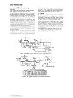
Figure 15 shows the basic connections for using an external
buffer amplifier to increase die output scale factor.
The output multiplied by the gain of the buffer, which is simply
the value of resistor R3 divided by RI. Choose a convenient
scale factor, keeping in mind that the buffer pin not only ampli-
fies the signal, but my noise or drift as well. Too much pin can
also cause the buffer to saturate and clip the output waveform.
Note that the “+” input of the external op amp uses the offset
null pin of the ADXL150/ADXL250 as a reference, biasing the
op amp at midsupply, saving two resistors and reducing power
consumption. The offset null pin connects to the V
S
/2 reference
point inside the accelerometer via 30 kΩ, so it is important not
to load this pin with more dim a few microamps.
It is important to use a single-supply or “rail-to-rail” op amp
for the external buffer as it needs to be able to swing close to
the supply and ground.
The circuit of Figure 15 is entirely adequate for many applica-
tions, but its accuracy is dependent on the pretrimmed accuracy
of the accelerometer and this will vary by product type and grade.
For the highest possible accuracy, an external trim is mended.
As shown by Figure 20, this consists of a potentiometer Rla,
in series with a fixed resistor, Rlb. Another to select resistor
values after measuring the device’s scale (see Figure 17).
AC Coupling
If a dc (gravity) response is not required—for example ** tion
measurement applications—ac coupling can be ** between the
accelerometer’s output and the external op** input as shown in
Figure 16. The use of ac coupling ** eliminates my zero g drift
and allows the maximum ** amp gain without clipping.
Resistor R2 and capacitor C3 together form a high ** whose
corner frequency is 1/(2 x R2 C3). This filter ** the signal from
the accelerometer by 3 dB at the **, and it will continue to
reduce it at a rate of 6 ** (20 dB per decade) for signals below
the corner frequ ** Capacitor CBS should be a nonpolarized,
low leakage type **
If ac coupling is used, the self-test feature must be ** the
accelerometer’s output rather than at the external ** output
(since the self-test output is a dc voltage).
© 2001 by CRC Press LLC
160
Chapter three: Structural design, modeling, and simulation
ADXL150/ADXL250
Adjusting the Zero g Bias Level
When a true dc (gravity) response is needed, the output from
the accelerometer must be dc coupled to the external amplifier’s
input. For high gain applications, a zero g offset trim will also
be needed. The external offset trim permits the user to set the
zew g offset voltage to exactly +2.5 volts (allowing the maxi-
mum output swing from the external amplifier without clipping
with a +5 supply).
With a dc coupled connection, any difference between the zero
g output and +2.5 V will be amplified along with the signal. To
obtain the exact zero g output desired or to allow the maximum
output voltage swing from the external amplifier, the zero g
offset will need to be externally trimmed using the circuit of
Figure 20.
The external amplifier’s maximum output swing should be
limited to ±2 volts, which provides a safety margin of ±0.25
volts before clipping. With a +2.5 volt zero g level, the maximum
gain will equal:
The device scale factor and zero g offset levels can be calibrated
using the earth’s gravity, as explained in the section “calibrating
the ADXL150/ADXL250.”
Using the Zero g “Quick-Cal” Method
In Figure 18 (accelerometer alone, no external op amp), a trim
potentiometer connects directly to the accelerometer’s zero g
null pin. The “quick offset calibration” scheme shown in Figure
17 is preferred over using a potentiometer, which could change
its setting over time due to vibration. The “quick offset calibra-
tion” method requires measuring only the output voltage of the
ADXL150/ADXL250 while it is oriented normal to the earth’s
gravity. Then, by using the simple equations shown in the fig-
ures, the correct resistance value for R2 can be calculated. In
Figure 17, an external op amp is used to amplify the signal. A
resistor, R2, is connected to the op amp’s summing junction.
The other side of R2 connects to either ground or +V
S
depending
on which direction the offset needs to be shifted.
DESIRED
OUTPUT
SCALE FACTOR
76mV/g
100mV/g
200mV/g
400mV/g
(a)
(b)
(c)
NOTES:
0g “QUICK” CALIBRATION METHOD USING RESISTOR R2 AND A +5V SUPPLY.
WITH ACCELEROMETER ORIENTED AWAY FROM EARTH’S
GRAVITY (i.e., SIDEWAYS), MEASURE PIN 10 OF THE ADXL150.
CALCULATE THE OFFSET VOLTAGE THAT NEEDS TO BE NULLED:
Figure 17. “Quick Zero g Calibration” Connection
V
OS
= (+2.5V − V
PIN
(10)(R3/R1).
R2 =
(d)
FOR V
PIN
10 > +2.5V, R2 CONNECTS TO GND.
(e)
FOR V
PIN
10 < +2.5V, R2 CONNECTS TO +V
S
.
2.5 V (R3)
V
OS
±25g
±20g
±10g
±5g
2.0
2.6
5.3
10.5
49.9kΩ
38.3kΩ
18.7kΩ
9.53kΩ
FS
RANGE
EXT
AMP
GAIN
R1
VALUE
2 Volts
38 mV/g Times the Max Applied Acceleration in g
---------------------------------------------------------------------------------------------------------------------------
Figure 18. Offset Nulling the ADXL150/ADXL250 Using a Trim Potentiometer
© 2001 by CRC Press LLC
Chapter three: Structural design, modeling, and simulation
161
ADXL150/ADXL250
DEVICE BANDWIDTH VS. MEASUREMENT
RESOLUTION
Although an accelerometer is usually specified according to its
full-scale g level, the limiting resolution of the device, i.e., its
minimum discernible input level, is extremely important when
measuring low g accelerations.
The limiting resolution is predominantly set by the measure-
ment noise “floor,” which includes the ambient background
noise and the noise of the ADXL150/ADXL250 itself. The level
of the noise floor varies directly with the bandwidth of the
measurement. As the measurement bandwidth is reduced, the
noise floor drops, improving the signal-to-noise ratio of the
measurement and increasing its resolution.
The bandwidth of the accelerometer can be easily reduced by
adding low-pass or bandpass filtering. Figure 19 shows the
typical noise vs. bandwidth characteristic of the ADXL150/
ADXL250.
The output noise of the ADXL150/ADXL250 scales with the
square root of the measurement bandwidth. With a single pole
roll-off, the equivalent rms noise bandwidth is π divided by 2
or approximately 1.6 times the 3 dB bandwidth. For example,
the typical rms noise of the ADXL150 using a 100 Hz one pole
post filter is:
Because the ADXL150/ADXL250’s noise is, for all practical
purposes, Gaussian in amplitude distribution, the highest noise
amplitudes have die smallest (yet nonzero) probability. Peak-
to-peak noise is therefore difficult to measure and can only be
estimated due to its statistical nature. Table I is useful for esti-
mating the probabilities of exceeding various peak values, given
the rms value.
RMS and peak-to-peak noise (for 0. 1% uncertainty) for various
bandwidths are estimated in Figure 19. As shown by the figure,
device noise drops dramatically as the operating bandwidth is
reduced. For example, when operated in a 1 kHz bandwidth,
the ADXL150/ADXL250 typically have an rms noise level of
32 mg. When the device bandwidth is rolled off to 100 Hz, the
noise level is reduced to approximately 10 mg.
Alternatively, the signal-to-noise ratio may be improved con-
siderably by using a microprocessor to perform multiple mea-
surements and then to compute the average signal level.
Low-Pass Filtering
The bandwidth of the accelerometer can easily be reduced by using
post filtering. Figure 20 shows how the buffer amplifier can be
connected to provide 1-pole post filtering, zero g offset trimming,
and output scaling. The table provides practical component values
Figure 19. ADXL150/ADXL250 Noise Level vs. 3 dB Band-
width (Using a “Brickwall” Filter)
TABLE I.
Nominal Peak-to-
Peak Value
% of Time that Noise Will Exceed
Nominal Peak-to-Peak Value
2.0 × rms
4.0 × rms
6.0 × rms
6.6 × rms
8.0 × rms
32%
4.6%
0.27%
0.1%
0.006%
Noise rms()1 mg/ Hz 100 1.6()× 12.25 mg==
Figure 20. One-Pole Post Filter Circuit with SF and Zero g Offset Trims
DESIRED
OUTPUT
SCALE FACTOR
76m/g
100m/g
200m/g
400m/g
±25g
±20g
±10g
±5g
2.0
2.6
5.3
10.5
200kΩ
261kΩ
536kΩ
1MΩ
0.0082
0.0056
0.0033
0.0015
0.027
0.022
0.010
0.0056
0.082
0.056
0.033
0.015
F. S.
RANGE
EXT
AMP
GAIN
R3
VALUE
Cf (µF)
100Hz
Cf (µF)
30Hz
Cf (µF)
10Hz
© 2001 by CRC Press LLC
162
Chapter three: Structural design, modeling, and simulation
ADXL150/ADXL250
for various full-scale g levels and approximate circuit band-
widths. For bandwidths other than those listed, use the
formula:
or simply scale the value of capacitor Cf accordingly; i.e., for
an application with a 50 Hz bandwidth, the value of Cf will
need to be twice as large as its 100 Hz value. If further noise
reduction is needed while maintaining the maximum possible
bandwidth, a 2- or 3-pole post filter is recommended. These
provide a much steeper roll-off of noise above the pole fre-
quency. Figure 21 shows a circuit that provides 2-pole post
filtering. Component values for the 2-pole filter were selected
to operate the first op amp at unity gain. Capacitors C3 and C4
were chosen to provide 3 dB bandwidths of 10 Hz, 30 Hz, 100 Hz
and 300 Hz.
The second op amp offsets and scales the output to provide a
+2.5 V ± 2 V output over a wide range of full-scale g levels.
APPLICATION HINTS
ADXL250 Power Supply Pins
When wiring the ADXL250, be sure to connect BOTH power
supply terminals, Pins 14 and 13.
Ratiometric Operation
Ratiometric operation means that the circuit uses the power
supply as its voltage reference. If the supply voltage varies, the
accelerometer and the other circuit components (such as an
ADC, etc.) track each other and compensate for the change.
Figure 22 shows how both the zero g offset and output sensi-
tivity of the ADXL150/ADXL250 vary with changes in supply
voltage. If they are to be used with nonratiometric devices, such
as an ADC with a built-in 5 V reference, then both components
should be referenced to the same source, in this case the ADC
reference. Alternatively, the circuit can be powered from an
external +5 volt reference.
Since any voltage variation is transferred to the accelerometer’s
output, it is important to reduce any power supply noise. Simply
following good engineering practice of bypassing the power
supply right at Pin 14 of the ADXL150/ADXL250 with a 0.1 µF
capacitor should be sufficient.
Cf
1
2πR3() Desired 3dB Bandwidth in Hz
---------------------------------------------------------------------------------------------=
Figure 22. Typical Ratiornetric Operation
Figure 21. Two-Pole Post Filter Circuit
© 2001 by CRC Press LLC
Chapter three: Structural design, modeling, and simulation
163
ADXL150/ADXL250
Additional Noise Reduction Techniques
Shielded wire should be used for connecting the accelerometer
to any circuitry that is more than a few inches away—to avoid
60 Hz pickup from ac line voltage. Ground the cable’s shield at
only one end and connect a separate common lead between the
circuits; this will help to prevent ground loops. Also, if the
accelerometer is inside a metal enclosure, this should be
grounded as well.
Mounting Fixture Resonances
A common source of error in acceleration sensing is resonance
of the mounting fixture. For example, the circuit board that the
ADXL150/ADXL250 mounts to may have resonant frequencies
in the same range as the signals of interest. This could cause
the signals measured to be larger than they really are. A common
solution to this problem is to damp these resonances by mount-
ing the ADXL150/ADXL250 near a mounting post or by adding
extra screws to hold the board more securely in place.
When testing the accelerometer in your end application, it is
recommended that you test the application at a variety of fre-
quencies to ensure that no major resonance problems exist.
REDUCING POWER CONSUMPTION
The use of a simple power cycling circuit provides a dramatic
reduction in the accelerometer’s average current consumption.
In low bandwidth applications such as shipping recorders, a
simple, low cost circuit can provide substantial power reduction.
If a microprocessor is available, it can supply a TTL clock pulse
to toggle the accelerometer’s power on and off.
A 10% duty cycle, 1 ms on, 9 ms off, reduces the average
current consumption of the accelerometer from 1.8 mA to 180
µA, providing a power reduction of 90%.
Figure 23 shows the typical power-on settling time of the
ADXL150/ADXL250.
CALIBRATING THE ADXL150/ADXL250
If a calibrated shaker is not available, both the zero g level and
scale factor of the ADXL150/ADXL250 may be easily set to fair
accuracy by using a self-calibration technique based on the 1 g
acceleration of the earth’s gravity. Figure 24 shows how gravity
and package orientation affect the ADXL150/ADXL250’s output.
With its axis of sensitivity in the vertical plane, the ADXL150/
ADXL250 should register a 1 g acceleration, either positive or
negative, depending on orientation. With the axis of sensitivity
in the horizontal plane, no acceleration (the zero g bias level)
should be indicated. The use of an external buffer amplifier may
invert the polarity of the signal.
Figure 24 shows how to self-calibrate the ADXL150/ADXL250.
Place the accelerometer on its side with its axis of sensitivity
oriented as shown in “a.” (For the ADXL250 this would be the
“X” axis—its “Y” axis is calibrated in the same manner, but the
part is rotated 90° clockwise.) The zero g offset potentiometer
RT is then roughly adjusted for midscale: +2.5 V at the external
amp output (see Figure 20).
Next, the package axis should be oriented as in “c” (pointing
down) and the output reading noted. The package axis should
then be rotated 180° to position “d” and the scale factor poten-
tiometer, Rlb, adjusted so that the output voltage indicates a
change of 2 gs in acceleration. For example, if the circuit scale
factor at the external buffer’s output is 100 mV per g, the scale
factor trim should be adjusted so that an output change of 200
mV is indicated.
Self-Test Function
A Logic “1” applied to the self-test (ST) input will cause an
electrostatic force to be applied to the sensor that will cause it
to deflect. If the accelerometer is experiencing an acceleration
when the self-test is initiated, the output will equal the algebraic
sum of the two inputs. The output will stay at the self-test level
as long as the ST input remains high, and will return to the
actual acceleration level when the ST voltage is removed.
Using an external amplifier to increase output scale factor may
cause the self-test output to overdrive the buffer into saturation.
The self-test may still be used in this case, but the change in
the output must then be monitored at the accelerometer’s output
instead of the external amplifier’s output.
Note that the value of the self-test delta is not an exact indication
of the sensitivity (mV/g) and therefore may not be used to
calibrate the device for sensitivity error.
Figure 23. Typical Power-On Settling with Full-Scale Input.
Time Constant of Post Filter Dominates the Response When
a Signal Is Present.
Figure 24. Using the Earth’s Gravity to Self-Calibrate the
ADXL150/ADXL250
© 2001 by CRC Press LLC
164
Chapter three: Structural design, modeling, and simulation
ADXL150/ADXL250
MINIMIZING EMI/RFI
The architecture of the ADXL150/ADXL250, and its use of syn-
chronous demodulation, makes the device immune to most elec-
tromagnetic (EMI) and radio frequency (RFI) interference. The
use of synchronous demodulation allows the circuit to reject all
signals except those at the frequency of the oscillator driving the
sensor element. However, the ADXL150/ADXL250 have a sen-
sitivity to noise on the supply lines that is near its internal clock
frequency (approximately 100 kHz) or its odd harmonics and can
exhibit baseband errors at the output. These error signals are the
beat frequency signals between the clock and the supply noise.
Such noise can be generated by digital switching elsewhere in
the system and must be attenuated by proper bypassing. By insert-
ing a small value resistor between the accelerometer and its power
supply, an RC filter is created. This consists of the resistor and
the accelerometer’s normal 0.1 µF bypass capacitor. For example
if R = 20 Ω and C = 0.1 µF, a filter with a pole at 80 kHz is
created, which is adequate to attenuate noise on the supply from
most digital circuits, with proper ground and supply layout.
Power supply decoupling, short component leads, physically
small (surface mount, etc.) components and attention to good
grounding practices all help to prevent RFI and EMI problems.
Good grounding practices include having separate analog and
digital grounds (as well as separate power supplies or very good
decoupling) on the printed circuit boards.
INTERFACING THE ADXL150/ADXL250 SERIES i
MEM
S
ACCELEROMETERS WITH POPULAR ANALOG-TO-
DIGITAL CONVERTERS.
Basic Issues
The ADXL150/ADXL250 Series accelerometers were designed
to drive popular analog-to-digital converters (ADCs) directly.
In applications where both a ±50 g full-scale measurement range
and a 1 kHz bandwidth are needed, the V
OUT
terminal of the
accelerometer is simply connected to the V
IN
terminal of the
ADC as shown in Figure 25a. The accelerometer provides its
(nominal) factory preset scale factor of +2.5 V ±38 mV/g which
drives the ADC input with +2.5 V ±1.9 V when measuring a 50 g
full-scale signal (38 mV/g × 50 g = 1.9 V).
As stated earlier, the use of post filtering will dramatically
improve the accelerometer’s low g resolution. Figure 25b shows
a simple post filter connected between the accelerometer and
the ADC. This connection, although easy to implement, will
require fairly large values of Cf, and the accelerometer’s signal
will be loaded down (causing a scale factor error) unless the
ADC’s input impedance is much greater than the value of Rf.
ADC input impedance’s range from less than 1.5 kΩ up to
greater than 15 kΩ with 5 kΩ values being typical. Figure 25c
is the preferred connection for implementing low-pass filtering
with the added advantage of providing an increase in scale
factor, if desired.
Calculating ADC Requirements
The resolution of commercial ADCs is specified in bits. In an
ADC, the available resolution equals 2
n
, where n is the number
of bits. For example, an 8-bit converter provides a resolution of
2
8
which equals 256. So the full-scale input range of the converter
divided by 256 will equal the smallest signal it can resolve.
In selecting an appropriate ADC to use with our accelerometer
we need to find a device that has a resolution better than the
measurement resolution but, for economy’s sake, not a great
deal better.
For most applications, an 8- or 10-bit converter is appropriate.
The decision to use a 10-bit converter alone, or to use a gain
stage together with an 8-bit converter, depends on which is more
important: component cost or parts count and ease of assembly,
Table II shows some of the tradeoffs involved.
Adding amplification between the accelerometer and the ADC
will reduce the circuit’s full-scale input range but will greatly
reduce the resolution requirements (and therefore the cost) of
the ADC. For example, using an op amp with a gain of 5.3
following the accelerometer will increase the input drive to the
ADC from 38 mV/g to 200 mV/g. Since the signal has been
gained up, but the maximum full-scale (clipping) level is still
the same, the dynamic range of the measurement has also been
reduced by 5.3.
Table III is a chart showing the required ADC resolution vs. the
scale factor of the accelerometer with or without a gain ampli-
fier. Note that the system resolution specified in the table refers
Table II.
8-Bit Converter and
Op Amp Preamp
10-bit (or 12-Bit)
Converter
Advantages:
Low Cost Converter No Zero g Trim Required
Disadvantages:
Needs Op Amp
Needs Zero g Trim
Higher Cost Converter
Table III. Typical System Resolution Using Some Popular
ADCs Being Driven with and without an Op Amp Preamp
Converter
Type 2
n
Converter
mV/Bit
(5 V/2
n
)
Preamp
Gain
SF
in
mV/g
FS
Range
in g’s
System
Resolution
in g’s (p-p)
8 Bit 256 19.5 mV None 38 ±50 0.51
256 19.5 mV 2 76 ±25 0.26
256 19.5 mV 2.63 100 ±20 0.20
256 19.5 mV 5.26 200 ±10 0.10
10 Bit 1,024 4.9 mV None 38 ±50 0.13
1,024 4.9 mV 2 76 ±25 0.06
1,024 4.9 mV 2.63 100 ±20 0.05
1,024 4.9 mV 5.26 200 ±10 0.02
12 Bit 4,096 1.2 mV None 38 ±50 0.03
4,096 1.2 mV 2 76 ±25 0.02
4,096 1.2 mV 2.63 100 ±20 0.01
4,096 1.2 mV 5.26 200 ±10 0.006
© 2001 by CRC Press LLC
Chapter three: Structural design, modeling, and simulation
165
ADXL150/ADXL250
to that provided by the converter and preamp (if used). It is
necessary to use sufficient post filtering with the accelerometer
to reduce its noise floor to allow full use of the converter’s
resolution (see post filtering section).
The use of a pin stage following the accelerometer will normally
require the user to adjust the zero g offset level (either by
trimming or by resistor selection—see previous sections).
For many applications, a modern “economy priced” 10-bit
converter, such as the AD7810 allows you to have high resolu-
tion without using a preamp or adding much to the overall circuit
cost. In addition to simplicity and cost, it also meets two other
necessary requirements: it operates from a single +5 V supply
and is very low power.
OUTLINE DIMENSIONS
Dimensions shows in inches and (mm).
14-Lead Cerpac
(QC-14)
Figure 25. Interfacing the ADXL150/ADXL250 Series Accel-
erometers to an ADC
© 2001 by CRC Press LLC
3.2. STRUCTURAL SYNTHESIS OF NANO- AND
MICROELECTROMECHANICAL ACTUATORS AND SENSORS
New advances in micromachining and microstructures, nano- and
microscale electromechanical devices, analog and digital ICs, provide
enabling benefits and capabilities to design and manufacture NEMS and
MEMS. Critical issues are to improve power and thermal management,
circuitry and actuator/sensor integration, as well as embedded electronically
controlled actuator/sensor assemblies. Very large scale integrated circuit and
micromachining silicon, germanium, and gallium arsenic technologies have
been developed and used to manufacture ICs and motion microstructures
(microscale actuators and sensors). While enabling technologies have been
developed to manufacture NEMS and MEMS, a spectrum of challenging
problems remains. Electromagnetics and fluid dynamic, quantum
phenomena, electro-thermo-mechanics and optics, biophysics and
biochemistry, mechanical and structural synthesis, analysis and optimization,
simulation and virtual prototyping, among other important problems, must be
thoroughly studied in nano- and microscale. There are several key focus
areas to be studied. In particular, structural synthesis and optimization,
fabrication, nonlinear model development and analysis, system design and
simulations.
An important problem addressed and studied in this section is the
structural synthesis of motion nano- and microstructures (shape/geometry
synthesis, optimization, and database developments). The proposed concept
allows the designer to generate optimal structures of actuators and sensors.
Using the proposed concept one can generate and optimize different nano-
and microdevices, perform modeling and simulations, etc. These directly
leverage high-fidelity model development and structural synthesis, allowing
the designer to attain physical and behavioral (steady-state and transient)
analysis, optimization, performance assessment, outcome prediction, etc.
3.2.1. Configurations and Structural Synthesis of Motion Nano- and
Microstructures (Actuators and Sensors)
Using the structural synthesis concept, nano-, micro-, and miniscale
actuators and sensors can be synthesized, analyzed, and optimized. In
particular, electromechanical/electromagnetic-based motion nano- and
microstructures (actuators and sensors) are classified using the specific
classifiers, and the structural synthesis can be performed based upon different
possible configurations, operating principles, phenomena, and physical laws.
We use the following electromagnetic systems
• endless (E),
• open-ended (O),
• integrated (I),
© 2001 by CRC Press LLC