Tài liệu Nano and Microelectromechanical Systems P1 ppt
Bạn đang xem bản rút gọn của tài liệu. Xem và tải ngay bản đầy đủ của tài liệu tại đây (159.52 KB, 22 trang )
CHAPTER 1
NANO- AND MICROENGINEERING,
AND NANO- AND MICROTECHNOLOGIES
1.1. INTRODUCTION
The development and deployment of NEMS and MEMS are critical to the
U.S. economy and society because nano- and microtechnologies will lead to
major breakthroughs in information technology and computers, medicine and
health, manufacturing and transportation, power and energy systems, and
avionics and national security. NEMS and MEMS have important impacts in
medicine and bioengineering (DNA and genetic code analysis and synthesis,
drug delivery, diagnostics, and imaging), bio and information technologies,
avionics, and aerospace (nano- and microscale actuators and sensors, smart
reconfigurable geometry wings and blades, space-based flexible structures, and
microgyroscopes), automotive systems and transportation (sensors and
actuators, accelerometers), manufacturing and fabrication, public safety, etc.
During the last years, the government and the high-technology industry have
heavily funded basic and applied research in NEMS and MEMS due to the
current and potential rapidly growing positive direct and indirect social and
economic impacts.
Nano- and microengineering are the fundamental theory, engineering
practice, and leading-edge technologies in analysis, design, optimization, and
fabrication of NEMS and MEMS, nano- and microscale structures, devices,
and subsystems. The studied nano- and microscale structures and devices
have dimensions of nano- and micrometers.
To support the nano- and microtechnologies, basic and applied research
and development must be performed. Nanoengineering studies nano- and
microscale-size materials and structures, as well as devices and systems, whose
structures and components exhibit novel physical (electromagnetic and
electromechanical), chemical, and biological properties, phenomena, and
processes. The dimensions of nanosystems and their components are 10
-10
m
(molecule size) to 10
-7
m; that is, 0.1 to 100 nanometers. Studying
nanostructures, one concentrates one’s attention on the atomic and molecular
levels, manufacturing and fabrication, control and dynamics, augmentation and
structural integration, application and large-scale system synthesis, et cetera.
Reducing the dimensions of systems leads to the application of novel materials
(carbon nanotubes, quantum wires and dots). The problems to be solved range
from mass-production and assembling (fabrication) of nanostructures at the
atomic/molecular scale (e.g., nanostructured electronics and actuators/sensors)
with the desired properties. It is essential to design novel nanodevices such as
nanotransistors and nanodiodes, nanoswitches and nanologic gates, in order
to design nanoscale computers with terascale capabilities. All living biological
© 2001 by CRC Press LLC
systems function due to molecular interactions of different subsystems. The
molecular building blocks (proteins and nucleic acids, lipids and
carbohydrates, DNA and RNA) can be viewed as inspiring possible strategy
on how to design high-performance NEMS and MEMS that possess the
properties and characteristics needed. Analytical and numerical methods are
available to analyze the dynamics and three-dimensional geometry, bonding,
and other features of atoms and molecules. Thus, electromagnetic and
mechanical, as well as other physical and chemical properties can be studied.
Nanostructures and nanosystems will be widely used in medicine and
health. Among possible applications of nanotechnology are: drug synthesis
and drug delivery (the therapeutic potential will be enormously enhanced due
to direct effective delivery of new types of drugs to the specified body sites),
nanosurgery and nanotherapy, genome synthesis and diagnostics, nanoscale
actuators and sensors (disease diagnosis and prevention), nonrejectable nano-
artificial organs design and implant, and design of high-performance
nanomaterials.
It is obvious that nano- and microtechnologies drastically change the
fabrication and manufacturing of materials, devices, and systems through:
•
predictable properties of nano composites and materials (e.g., light
weight and high strength, thermal stability, low volume and size,
extremely high power, torque, force, charge and current densities,
specified thermal conductivity and resistivity, et cetera),
•
virtual prototyping (design cycle, cost, and maintenance reduction),
•
improved accuracy and precision, reliability and durability,
•
higher degree of efficiency and capability, flexibility and integrity,
supportability and affordability, survivability and redundancy,
•
improved stability and robustness,
•
higher degree of safety,
•
environmental competitiveness.
Foreseen by Richard Feyman, the term “nanotechnology” was first used
by N. Taniguchi in his 1974 paper, "On the basic concept of
nanotechnology." In the last two decades, nanoengineering and
nanomanufacturing have been popularized by Eric Drexler through the
Foresight Institute.
Advancing miniaturization towards the molecular level with the ultimate
goal to design and manufacture nanocomputers and nanomanipulators
(nanoassemblers), large-scale intelligent NEMS and MEMS (which have
nanocomputers as the core components), the designer faces a great number of
unsolved problems.
Possible basic concepts in the development of nanocomputers are listed
below. Mechanical “computers” have the richest history traced thousand
years back. While the most creative theories and machines have been
developed and demonstrated, the feasibility of mechanical nanocomputers is
questioned by some researchers due to the number of mechanical
components (which are needed to be controlled), as well as due to unsolved
© 2001 by CRC Press LLC
manufacturing (assembling) and technological difficulties. Chemical
nanocomputers can be designed based upon the processing information by
making or breaking chemical bonds, and storing the information in the
resulting chemical. In contrast, in quantum nanocomputers, the information
can be represented by a quantum state (e.g., the spin of the atom can be
controlled by the electromagnetic field).
Electronic nanocomputers can be designed using conventional concepts
tested and used for the last thirty years. In particular, molecular transistors or
quantum dots can be used as the basic elements. The nanoswitches
(memoryless processing elements), logic gates, and registers must be
manufactured on the scale of a single molecule. The so-called quantum dots
are metal boxes that hold the discrete number of electrons which is changed
applying the electromagnetic field. The quantum dots are arranged in the
quantum dot cells. Consider the quantum dot cells which have five dots and
two quantum dots with electrons. Two different states are illustrated in
Figure 1.1.1 (the dashed dots contain the electron, while the white dots do
not contain the electron). It is obvious that the quantum dots can be used to
synthesize the logic devices.
Figure 1.1.1. Quantum dots with states “0” and “1”, and “1 1” configuration
It was emphasized that as conventional electromechanical systems,
nanoelectromechanical systems (actuators and other molecular devices) are
controlled by changing the electromagnetic field. It becomes evident that
other nanoscale structures and devices (nanodiodes and nanotransistors) are
also controlled by applying the electromagnetic field (recall that the voltage
and current result due to the electromagnetic field).
1.2. BIOLOGICAL ANALOGIES
Coordinated behavior and motion, visualization and sensing, motoring
and decision making, memory and learning of living organisms are the results
of the electrical (electromagnetic) transmission of information by neurons.
One cubic centimeter of the brain contains millions of nerve cells, and these
cells communicate with thousands of neurons creating data processing
(communication) networks. The information from the brain to the muscles is
transmitted within the milliseconds, and the baseball and football, basketball,
"1" "1"State "0" State "1"
© 2001 by CRC Press LLC
and tennis players calculate the speed and velocity of the ball, analyze the
situation, make the decision, and respond (e.g., run or jump, throw or hit the
ball, et cetera). Human central nervous system, which includes brain and
spinal cord, serves as the link between the sensors (sensor receptors) and
motors peripheral nervous system (effector, muscle, and gland cells). It
should be emphasized that the nervous system has the following major
functions: sensing, integration and decision making (computing), and
motoring (actuation). Human brain consists of hindbrain (controls
homeostasis and coordinate movement), midbrain (receiving, integration, and
processing the sensory information), and forebrain (neural processing and
integration of information, image processing, short- and long-term memories,
learning functions, decision making and motor command development). The
peripheral nervous system consists of the sensory system (sensory neurons
transmit information from internal and external environment to the central
nervous system, and motor neurons carry information from the brain or
spinal cord to effectors), which supplies information from sensory receptors
to the central nervous system, and the motor nervous system feeds signals
(commands) from the central nervous system to muscles (effectors) and
glands. The spinal cord mediates reflexes that integrate sensor inputs and
motor outputs, and through the spinal cord the neurons carry information to
and from the brain. The transmission of electrical signals along neurons is a
very complex phenomenon. The membrane potential for a nontransmitting
neuron is due to the unequal distribution of ions (sodium and potassium)
across the membrane. The resting potential is maintained due to the
differential ion permeability and the so-called Na
+
- K
+
pump. The stimulus
changes the membrane permeability, and ion can depolarize or hyperpolarize
the membrane resting potential. This potential (voltage) change is
proportional to the strength of the stimulus. The stimulus is transmitted due
to the axon mechanism. The nervous system is illustrated in Figure 1.2.1.
Figure 1.2.1. Vertebrate nervous system: high-level functional diagram
There is a great diversity of the nervous system organizations. The
cnidarian (hydra) nerve net is an organized system of nerves with no central
Nervous System
Peripheral Nervous
System
Central Nervous
System
Brain Spinal Cord
Sensor
System
Motor
System
© 2001 by CRC Press LLC
control, and a simple nerve net can perform elementary tasks (jellyfishes
swim). Echinoderms have a central nerve ring with radial nerves (for
example, sea stars have central and radial nerves with nerve net). Planarians
have small brains that send information through two or more nerve trunks, as
illustrated in Figure 1.2.2.
Figure 1.2.2. Overview of invertebrate nervous systems
1.3. NANO- AND MICROELECTROMECHANICAL SYSTEMS
Through biosystems analogy, a great variety of man-made
electromechanical systems have been designed and made. To analyze, design,
develop, and deploy novel NEMS and MEMS, the designer must synthesize
advanced architectures, integrate the latest advances in nano- and microscale
actuators/sensors (transducers) and smart structures, integrated circuits (ICs)
and multiprocessors, materials and fabrications, structural design and
optimization, modeling and simulation, et cetera. It is evident that novel
optimized NEMS and MEMS architectures (with processors or
multiprocessors, memory hierarchies and multiple parallelism to guarantee
high-performance computing and decision making), new smart structures and
actuators/sensors, ICs and antennas, as well as other subsystems play a critical
role in advancing the research, developments, and implementation. In this book
we discuss optimized architectures, and the research in architecture
optimization will provide deep insights into how intelligent large-scale
integrated NEMS and MEMS can be synthesized.
Electromechanical systems, as shown in Figure 1.3.1, can be classified as
•
conventional electromechanical systems,
•
microelectromechanical systems (MEMS),
•
nanoelectromechanical systems (NEMS).
Nerve
Trunk
Brain
Ring
of Nerve
Radial Nerves
Nerve Net
cnidarian echinoderm planarian
© 2001 by CRC Press LLC
Figure 1.3.1. Classification of electromechanical systems
The operational principles and basic foundations of conventional
electromechanical systems and MEMS are the same, while NEMS are
studied using different concepts and theories. In fact, the designer applies the
classical Lagrangian and Newtonian mechanics as well as electromagnetics
(Maxwell’s equations) to study conventional electromechanical systems and
MEMS. In contrast, NEMS are studied using quantum theory and
nanoelectromechanical concepts. Figure 1.3.2 documents the fundamental
theories to study the processes and phenomena in conventional, micro, and
nanoelectromechanical systems.
Figure 1.3.2. Fundamental theories in electromechanical systems
Conventional
Electromechanical
Systems
Micro-
electromechanical
Systems
Nano-
electromechanical
Systems
Fundamental Theories:
Classical Mechanics
Electromagnetics
Fundamental Theories:
Quantum Theory
Nanoelectromechanics
Electromechanical
Systems
Electromechanical
Systems
Conventional
Electromechanical
Systems
Micro-
electromechanical
Systems
Nano-
electromechanical
Systems
© 2001 by CRC Press LLC
NEMS and MEMS integrate different structures, devices, and subsystems.
The research in integration and optimization (optimized architectures and
structural optimization) of these subsystems has not been instituted and
performed, and end-to-end (processors – networks – input/output subsystems –
ICs/antennas – actuators/sensors) performance and behavior must be studied.
Through this book we will study different NEMS and MEMS architectures, and
fundamental and applied theoretical concepts will be developed and
documented in order to design next generation of superior high-performance
NEMS and MEMS.
The large-scale NEMS and MEMS, which can integrate processor
(multiprocessor) and memories, high-performance networks and input-output
(IO) subsystems, are of far greater complexity than MEMS commonly used
today. In particular, the large-scale NEMS and MEMS can integrate:
•
thousands of nodes of high-performance actuators/sensors and smart
structures controlled by ICs and antennas;
•
high-performance processors or superscalar multiprocessors;
•
multi-level memory and storage hierarchies with different latencies
(thousands of secondary and tertiary storage devices supporting data
archives);
•
interconnected, distributed, heterogeneous databases;
•
high-performance communication networks (robust, adaptive intelligent
networks).
It must be emphasized that even the simplest nanosystems (for example,
pure actuator) usually cannot function alone. For example, at least the internal
or external source of energy is needed.
The complexity of large-scale NEMS and MEMS requires new
fundamental and applied research and developments, and there is a critical need
for coordination across a broad range of hardware and software. For example,
design of advanced nano- and microscale actuators/sensors and smart
structures, synthesis of optimized (balanced) architectures, development of new
programming languages and compilers, performance and debugging tools,
operating system and resource management, high-fidelity visualization and data
representation systems, design of high-performance networks, et cetera. New
algorithms and data structures, advanced system software and distributed access
to very large data archives, sophisticated data mining and visualization
techniques, as well as advanced data analysis are needed. In addition, advanced
processor and multiprocessors are needed to achieve sustained capability
required of functionally usable large-scale NEMS and MEMS.
The fundamental and applied research in NEMS and MEMS has been
dramatically affected by the emergence of high-performance computing.
Analysis and simulation of NEMS and MEMS have significant outcomes. The
problems in analysis, modeling, and simulation of large-scale NEMS and
MEMS that involves the complete molecular dynamics cannot be solved
because the classical quantum theory cannot be feasibly applied to complex
molecules or simplest nanostructures (1 nm cube of nanoactuator has thousands
© 2001 by CRC Press LLC
of molecules). There are a number of very challenging research problems in
which advanced theory and high-end computing are required to advance the
theory and engineering practice. The multidisciplinary fundamentals of
nanoelectromechanics must be developed to guarantee the possibility to
synthesize, analyze, and fabricate high-performance NEMS and MEMS with
desired (specified) performance characteristics. This will dramatically shorten
the time and cost of developments of NEMS and MEMS for medical and
biomedical, aerospace and automotive, electronic and manufacturing systems.
The importance of mathematical model developments and numerical
analysis has been emphasized. Numerical simulation enhances, but does not
substitute for fundamental research. Furthermore, meaningful and explicit
simulations should be based on reliable fundamental studies and must be
validated through experiments. However, it is evident that simulations lead to
understanding of performance of complex NEMS and MEMS (nano- and
microscale structures, devices, and sub-systems), reduce the time and cost of
deriving and leveraging the NEMS and MEMS technologies from concept to
device/system, and from device/system to market. Fundamental and applied
research is the core of the simulation, and focused efforts must be concentrated
on comprehensive modeling and advanced efficient computing.
To comprehensively study NEMS and MEMS, advanced modeling and
computational tools are required primarily for 3D+ (three-dimensional
geometry dynamics in time domain) data intensive modeling and simulations to
study the end-to-end dynamic behavior of actuators and sensors. The
mathematical models of NEMS, MEMS, and their components (structures,
devices, and subsystems) must be developed. These models (augmented with
efficient computational algorithms, terascale computers, and advanced
software) will play the major role to simulate the design of NEMS and MEMS
from virtual prototyping standpoints.
There are three broad categories of problems for which new algorithms
and computational methods are critical:
1.
Problems for which basic fundamental theories are developed, but the
complexity of solutions is beyond the range of current and near-future
computing technologies. For example, the conceptually straightforward
classical quantum mechanics and molecular dynamics cannot be applied
even for nanoscale actuators. In contrast, it will be illustrated that it is
possible to perform robust predictive simulations of molecular-scale
behavior for nano- and microscale actuators/sensors and smart structures
which might contain millions of molecules.
2.
Problems for which fundamental theories are not completely developed to
justify direct simulations, but can be advanced or developed by advanced
basic and numerical methods.
3.
Problems for which the developed advanced modeling and simulation
methods will produce major advances and will have a major impact. For
example, 3D+ transient end-to-end behavior of NEMS and MEMS.
For NEMS and MEMS, as well as for their devices and subsystems,
© 2001 by CRC Press LLC
high-fidelity modeling and massive computational simulations (mathematical
models designed with developed intelligent libraries and databases/archives,
intelligent experimental data manipulation and storage, data grouping and
correlation, visualization, data mining and interpretation) offer the promise of
developing and understanding the mechanisms, phenomena and processes in
order to improve efficiency and design novel high-performance NEMS and
MEMS. Predictive model-based simulations require terascale computing and an
unprecedented level of integration between engineering and science. These
modeling and simulations will lead to new fundamental results. To model and
simulate NEMS and MEMS, we augment modern quantum mechanics,
electromagnetics, and electromechanics at the nano- and microscale. In
particular, our goal is to develop the nanoelectromechanical theory.
One can perform the steady-state and dynamic analysis. While steady-state
analysis is important, and the structural optimization to comprehend the
actuators/sensors, smart structures, and antennas design can be performed,
NEMS and MEMS must be analyzed in the time domain. The long-standing
goal of nanoelectromechanics is to develop the basic fundamental conceptual
theory in order to determine and study the interactions between actuation and
sensing, computing and communication, signal processing and hierarchical data
storage (memories), and other processes and phenomena in NEMS and MEMS.
Using the concept of strong electromagnetic-electromechanical interactions, the
fundamental nanoelectromechanical theory will be developed and applied to
nanostructures and nanodevices, NEMS and MEMS to predict the performance
through analytical solutions and numerical simulations. Dynamic macromodels
of nodes can be developed, and single and groups of molecules can be studied.
It is critical to perform this research in order to determine a number of the
parameters to make accurate performance evaluation and to analyze the
phenomena performing simulations and comparing experimental, modeling and
simulation results.
Current advances and developments in modeling and simulation of
complex phenomena in NEMS and MEMS are increasingly dependent upon
new approaches to robustly map, compute, visualize, and validate the results
clarifying, correlating, defining, and describing the limits between the
numerical results and the qualitative-quantitative analytic analysis in order to
comprehend, understand, and grasp the basic features. Simulations of NEMS
and MEMS require terascale computing that will be available within a couple
of years. The computational limitations and inability to develop explicit
mathematical models (some nonlinear phenomena cannot be comprehended,
fitted, and precisely mapped) focus advanced studies on the basic research in
robust modeling and simulation under uncertainties. Robust modeling,
simulation, and design are critical to advance and foster the theoretical and
engineering enterprises. We focus our research on the development of the
nanoelectromechanical theory in order to model and simulate large-scale
NEMS and MEMS. At the subsystem level, for example, nano- and microscale
actuators and sensors will be modeled and analyzed in 3D+ (three-dimensional
© 2001 by CRC Press LLC
geometry dynamics in time domain) applying advanced numerical robust
methods and algorithms. Rigorous methods for quantifying uncertainties for
robust analysis should be developed. Uncertainties result due to the fact that it
is impossible to explicitly comprehend the complex interacted subsystems and
processes in NEMS and MEMS (actuators/sensors and smart structures,
antennas, digital and analog ICs, data movement, storage and management
across multilevel memory hierarchies, archives, networks and periphery),
structural and environmental changes, unmeasured and unmodeled phenomena,
et cetera.
To design NEMS and MEMS, we will develop analytical mathematical
models. There are a number of areas where the advances must be made in order
to realize the promises and benefits of modern theoretical developments
recently made. For example, to perform 3D+ modeling and data intensive
simulations of actuators/sensors and smart structures, we will use advanced
analytical and numerical methods and algorithms (novel methods and
algorithms in geometry and mesh generation, data assimilation, and dynamic
adaptive mesh refinement) as well as the computationally efficient and robust
M
ATLAB
environment. There are fundamental and computational problems that
have not been addressed, formulated and solved due to the complexity of large-
scale NEMS and MEMS (e.g., large-scale hybrid models, limited ability to
generate and visualize the massive amount of data, et cetera). Other problems
include nonlinearities and uncertainties which imply fundamental limits to
formulate, set up, and solve analysis and design problems. Therefore, one
should develop rigorous methods and algorithms for quantifying and modeling
uncertainties, 3D+ geometry and mesh generation techniques, as well as
methods for adaptive robust modeling and simulations under uncertainties. A
broad class of fundamental and applied problems ranging from fundamental
theories (quantum mechanics and electromagnetics, electromechanics and
thermodynamics, structural synthesis and optimization, optimized architecture
design and control, modeling and analysis, et cetera) and numerical computing
(to enable the major progress in design and virtual prototyping through the
large scale simulations, data intensive computing, and visualization) will be
addressed and thoroughly studied in this book. Due to the obvious limitations
and the scope of this book, a great number of problems and phenomena will not
be addressed and discussed (among them, fabrication and manufacturing,
chemistry and material science).
1.4.
APPLICATIONS OF NANO- AND
MICROELECTROMECHANICAL SYSTEMS
Depending upon the specifications and requirements, objectives and
applications, NEMS and MEMS must be designed. Usually, NEMS are faster
and simpler, more efficient and reliable, survivable and robust compared
with MEMS. However, due to the limited size and functional capabilities,
one might not attain the desired characteristics. For example, consider nano-
© 2001 by CRC Press LLC
and microscale actuators. The actuator size is determined by the force or
torque densities. That is, the size is determined by the force or torque
requirements and materials used. As one uses NEMS or MEMS as the logic
devices, the output electric signal (voltage or current) or electromagnetic
field (intensity or density) must have the specified value.
Although NEMS and MEMS have the common features, the differences
must be emphasized as well. Currently, the research and developments in
NEMS and molecular nanotechnology are primarily concentrated on design,
modeling, simulation, and fabrication of molecular-scale devices. In contrast,
MEMS are usually fabricated using other technologies, for example,
complementary metal oxide semiconductor (CMOS) and lithography. The
direct chip attaching technology was developed and widely deployed. Flip-chip
assembly replaces wire banding to connect ICs with micro- and nanoscale
actuators and sensors. The use of flip-chip technology allows one to eliminate
parasitic resistance, capacitance, and inductance. This results in improvements
of performance characteristics. In addition, flip-chip assembly offers
advantages in the implementation of advanced flexible packaging, improving
reliability and survivability, reduces weight and size, et cetera. The flip-chip
assembly involves attaching actuators and sensors directly to ICs. The actuators
and sensors are mounted face down with bumps on the pads that form electrical
and mechanical joints to the ICs substrate. The under-fill encapsulate is then
added between the chip surface and the flex circuit to achieve the high
reliability demanded. Figure 1.4.1 illustrates flip-chip MEMS.
IC
SensorActuator
−
Actuator
Sensor
Figure 1.4.1. Flip-chip monolithic MEMS with actuators and sensors
The large-scale integrated MEMS (a single chip that can be mass-produced
using the complementary metal oxide semiconductor (CMOS),
photolithography, and other technologies at low cost) integrates:
•
N nodes of actuators/sensors, smart structures,
•
ICs and antennas,
•
processor and memories,
•
interconnection networks (communication busses),
•
input-output (IO) systems.
Different architectures can be synthesized, and this problem is discussed
© 2001 by CRC Press LLC
and covered in Chapter 2. One uses NEMS and MEMS to control complex
systems, processes, and phenomena. A high-level functional block diagram
of large-scale MEMS is illustrated in Figure 1.4.2.
Figure 1.4.2. High-level functional block diagram of large-scale MEMS
with rotational and translational actuators and sensors
Actuators are needed to actuate dynamic systems. Actuators respond to
command stimulus (control signals) and develop torque and force. There is a
great number of biological (e.g., human eye and locomotion system) and man-
made actuators. Biological actuators are based upon electromagnetic-
mechanical-chemical phenomena and processes. Man-made actuators
(electromagnetic, electric, hydraulic, thermo, and acoustic motors) are devices
that receive signals or stimulus (stress or pressure, thermo or acoustic, et cetera)
and respond with torque or force.
Consider the flight vehicles. The aircraft, spacecraft, missiles, and
interceptors are controlled by displacing the control surfaces as well as by
changing the control surface and wing geometry. For example, ailerons,
elevators, canards, flaps, rudders, stabilizers and tips of advanced aircraft can
be controlled by nano-, micro-, and miniscale actuators using the NEMS- and
Data
Acquisition
Sensors
Antennas
Amplifiers
ICs
VariablesMeasured
Actuators
Analysisand
Decision
System
Dynamic
Controller
Output
VariablesSystem
Criteria
Objectives
VariablesMEMS
SensorActuator
−
MEMS
SensorActuator
−
SensorActuator
−
IO
© 2001 by CRC Press LLC
MEMS-based smart actuator technology. This NEMS- and MEMS-based
smart actuator technology is uniquely suitable in the flight actuator
applications. Figure 1.4.3 illustrates the aircraft where translational and
rotational actuators are used to actuate the control surfaces, as well as to
change the wing and control surface geometry.
Figure 1.4.3. Aircraft with NEMS- and MEMS-based translational and
rotational flight actuators
Sensors are devices that receive and respond to signals or stimulus. For
example, the loads (which the aircraft experience during the flight),
vibrations, temperature, pressure, velocity, acceleration, noise, and radiation
can be measured by micro- and nanoscale sensors, see Figure 1.4.4. It should
be emphasized that there are many other sensors to measure the
electromagnetic interference and displacement, orientation and position,
voltages and currents in power electronic devices, et cetera.
ψφθ
,,
:AnglesEuler
ActuatorsFlight
BasedMEMSandNEMS
−−
SensorActuator
−
SensorActuator
−
GeometryWing
GeometrySurface
ntDisplacemeSurface
Control :
© 2001 by CRC Press LLC
Figure 1.4.4. Application of nano- and microscale sensors in aircraft
Usually, several conversion processes are involved to produce electric,
electromagnetic, or mechanical output sensor signals. The conversion of
energy is our particular interest. Using the energy-based analysis, the general
theoretical fundamentals will be thoroughly studied.
The major developments in NEMS and MEMS have been fabrication
technology driven, and the applied research has been performed mainly to
manufacture structures and devices, as well as to analyze some performance
characteristics. For example, mini- and microscale smart structures as well as
ICs have been studied in details, and feasible manufacturing technologies,
materials, and processes have been developed. Recently, carbon nanotubes
were discovered, and molecular wires and molecular transistors were built.
However, to our best knowledge, nanostructures and nanodevices, NEMS
and MEMS, have not been comprehensively studied at the nanoscale, and the
efforts to develop the fundamental theory have not been reported. In this
book, we will apply the quantum theory and charge density concept,
advanced electromechanics and Maxwell's equations, as well as other
cornerstone methods, to model nanostructures and nanodevices (ICs and
antennas, actuators and sensors, et cetera). In particular, the
nanoelectromechanical theory will be developed. A large variety of actuators
and sensors, antennas and ICs with different operating features are modeled
and simulated. To perform high-fidelity integrated 3D+ data intensive
modeling with post-processing and animation, the partial and ordinary
nonlinear differential equations are solved.
ψφθ
,,
:AnglesEuler
Radiation
Sensors
Noise
onAccelerati
Velocity
ressureP
Vibrations
Loads
eTemperatur
Flight Computer
SensorActuator
−
SensorActuator
−
© 2001 by CRC Press LLC
1.5. NANO- AND MICROELECTROMECHANICAL SYSTEMS
In general, monolithic MEMS are integrated microassembled structures
(electromechanical microsystems on a single chip) that have both electrical-
electronic (ICs) and mechanical components. To manufacture MEMS,
advanced modified microelectronics fabrication techniques, technologies,
and materials are used. Actuation and sensing cannot be viewed as the
peripheral function in many applications. Integrated sensors-actuators
(usually motion microstructures) with ICs compose the major class of
MEMS. Due to the use of CMOS lithography-based technologies in
fabrication actuators and sensors, MEMS leverage microelectronics in
important additional areas that revolutionize the application capabilities. In
fact, MEMS have considerably leveraged the microelectronics industry
beyond ICs. The needs for augmented motion microstructures (actuators and
sensors) and ICs have been widely recognized. Simply scaling conventional
electromechanical motion devices and augmenting them with ICs have not
met the needs, and theory and fabrication processes have been developed
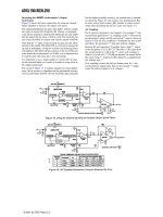
beyond component replacement. Dual power operational amplifiers (e.g.,
Motorola TCA0372, DW Suffix plastic package case 751G, DP2 Suffix
plastic package case 648 or DP1 Suffix plastic package case 626) as
monolithic ICs can be used to control DC micro electric machines (motion
microstructures), as shown in Figure 1.5.1.
Figure 1.5.1. Application of monolithic IC to control DC
micromachines (motion microstructures)
Only recently has it become possible to manufacture MEMS at low cost.
However, there is a critical demand for continuous fundamental, applied, and
technological improvements, and multidisciplinary activities are required.
The general lack of synergy theory to augment actuation, sensing, signal
processing, and control is known, and these issues must be addressed through
+
−
1
R
1
V
+
−
C
2
R
3
R
DeviceMotion DC
alromechanicMicroelect
2
V
ICs Monolithic
© 2001 by CRC Press LLC
focussed efforts. The set of long-range goals that challenge the analysis,
design, development, fabrication, and deployment of high-performance
MEMS are:
•
advanced materials and process technology,
•
microsensors and microactuators (motion microstructures), sensing and
actuation mechanisms, sensors-actuators-ICs integration and MEMS
configurations,
•
fabrication, packaging, microassembly, and testing,
•
MEMS analysis, design, optimization, and modeling,
•
MEMS applications and their deployment.
Significant progress in the application of CMOS technology enables the
industry to fabricate microscale actuators and sensors with the corresponding
ICs, and this guarantees the significant breakthrough. The field of MEMS has
been driven by the rapid global progress in ICs, VLSI, solid-state devices,
materials, microprocessors, memories, and DSPs that have revolutionized
instrumentation, control, and systems design philosophy. In addition, this
progress has facilitated explosive growth in data processing and
communications in high-performance systems. In microelectronics, many
emerging problems deal with nonelectric effects, phenomena and processes
(thermal and structural analysis and optimization, stress and ruggedness,
packaging, et cetera). It has been emphasized that ICs are the necessary
components to perform control, data acquisition, and decision making. For
example, control signals (voltage or currents) are computed, converted,
modulated, and fed to actuators. It is evident that MEMS have found
applications in a wide array of microscale devices (accelerometers, pressure
sensors, gyroscopes, et cetera) due to extremely-high level of integration of
electromechanical components with low cost and maintenance, accuracy,
efficiency, reliability, ruggedness, and survivability. Microelectronics with
integrated sensors and actuators are batch-fabricated as integrated
assemblies.
Therefore, MEMS can be defined as
batch-fabricated microscale
devices (ICs and motion microstructures) that convert physical parameters
to electrical signals and vice versa, and in addition, microscale features of
mechanical and electrical components, architectures, structures, and
parameters are important elements of their operation and design.
The manufacturability issues in NEMS and MEMS must be addressed.
One can design and manufacture individually-fabricated devices and
subsystems (ICs and motion microstructures). However, these individually-
fabricated devices and subsystems are unlikely can be used due to very high
cost.
Integrated MEMS combine mechanical structures (microfabricated smart
multifunctional materials are used to manufacture microscale actuators and
sensors, pumps and valves, optical devices) and microelectronics (ICs). The
number of transistors on a chip is frequently used by the microelectronic
industry, and enormous progress in achieving nanoscale transistor dimensions
© 2001 by CRC Press LLC
(less than 100 nm) was achieved. However, large-scale MEMS operational
capabilities are measured by the intelligence, system-on-a-chip integration,
integrity, cost, performance, efficiency, size, reliability, and other criteria.
There are a number of challenges in MEMS fabrication because conventional
CMOS technology must be modified and integration strategies (to integrate
mechanical structures and ICs) are needed to be developed. What (ICs or
mechanical micromachined structure) should be fabricated first? Fabrication of
ICs first faces challenges because to reduce stress in the thin films of
polysilicon (multifunctional material to build motion microstructures), a high-
temperature anneal at 1000
0
C is needed for several hours. The aluminum ICs
interconnect will be destroyed (melted), and tungsten can be used for
interconnected metallization. This process leads to difficulties for commercially
manufactured MEMS due to high cost and low reproducibility. Analog Devices
fabricates ICs first up to metallization step, and then, mechanical structures
(polysilicon) are built using high-temperature anneal (micromachines are
fabricated before metallization), and finally, ICs are interconnected. This allows
the manufacturer to use low-cost conventional aluminum interconnects. The
third option is to fabricate mechanical structures, and then ICs. However, to
overcome step coverage, stringer, and topography problems, motion
mechanical microstructures can be fabricated in the bottoms of the etched
shallow trenches (packaged directly) of the wafer. These trenches are filled with
a sacrificial silicon dioxide, and the silicon wafer is planarized through
chemical-mechanical polishing.
The motion mechanical microstructures can be protected (sensor
applications, e.g., accelerometers and gyroscopes) and unprotected (actuator
and interactive environment sensor applications). Therefore, MEMS
(mechanical structure – ICs) can be encased in a clean, hermetically sealed
package or some elements can be unprotected to interact with environment.
This creates challenges in packaging. It is extremely important to develop novel
electromechanical motion microstructures and microdevices (sticky multilayers,
thin films, magnetoelectronic, electrostatic, and quantum-effect-based devices)
and sense their properties. Microfabrication of very large scale integrated
circuits (VLSI), MEMS, and optoelectronics must be addressed. Fabrication
processes include lithography, film growth, diffusion, ion implantation, thin
film deposition, etching, metallization, et cetera. Furthermore, ICs and motion
microstructures (microelectromechanical motion devices) must be connected.
Complete microfabrication processes with integrated process steps must be
developed.
Microelectromechanical systems integrate microscale subsystems (at least
ICs and motion structure). It was emphasized that microsensors sense the
physical variables, and microactuators control (actuate) real-world systems.
These microactuators are regulated by ICs. It must be emphasized that ICs also
performed computations, signal conditioning, decision making, and other
© 2001 by CRC Press LLC
functions. For example, in microaccelerometers, the motion microstructure
displaces. Using this displacement, the acceleration can be calculated. In
microaccelerometers, computations, signal conditioning, data acquisition, and
decision making are performed by ICs. Microactuators inflate air-bags if car
crashes (high g acceleration measured).
Microelectromechanical systems contain microscale subsystems designed
and manufactured using different technologies. Single silicon substrate can be
used to fabricate microscale actuators, sensors, and ICs (monolithic MEMS)
using CMOS microfabrication technology. Alternatively, subsystem can be
assembled, connected and packaged, and different microfabrication techniques
for MEMS components and subsystems exist. Usually, monolithic MEMS are
compact, efficient, reliable, and guarantee superior performance.
Typically, MEMS integrate the following subsystems: microscale actuators
(actuate real-world systems), microscale sensors (detect and measure changes
of the physical variables), and microelectronics/ICs (signal processing, data
acquisition, decision making, et cetera).
Microactuators are needed to develop force or torque (mechanical
variable). Typical examples are microscale drives, moving mirrors, pumps,
servos, valves, et cetera. A great variety of methods for achieving actuation are
well-known, e.g., electromagnetic (electrostatic, magnetic, piezoelectric),
hydraulic, and thermal effects. This book covers electromagnetic
microactuators, and the so-called comb drives (surface micromachined motion
microstructures) have been widely used. These drives have movable and
stationary plates (fingers). When the voltage is applied, an attractive force is
developed between two plates, and the motion results. A wide variety of
microscale actuators have been fabricated and tested. The common problem is
the difficulties associated with coil fabrication. The choice of magnetic
materials (permanent magnets) is limited to those that can be micromachined.
Magnetic actuators typically fabricated through the photolithography
technology using nickel (ferromagnetic material). Piezoelectric microactuators
have found wide applications due to simplicity and ruggedness (force is
generated if one applies the voltage across a film of piezoelectric material). The
piezoelectric-based concept can be applied to thin silicon membranes, and if the
voltage is applied, the membrane deforms. Thus, silicon membranes can be
used as pumps.
Microsensors are devices that convert one physical variable (quantity) to
another. For example, electromagnetic phenomenon can be converted to
mechanical or optic effects. There are a number of different types of microscale
sensors used in MEMS. For example, microscale thermosensors are designed
and built using the thermoelectric effect (the resistivity varies with
temperature). Extremely low cost thermoresistors (thermistors) are fabricated
on the silicon wafer, and ICs are built on the same substrate. The thermistor
resistivity is a highly nonlinear function of the temperature, and the
compensating circuitry is used to take into account the nonlinear effect.
Microelectromagnetic sensors measure electromagnetic fields, e.g., the Hall
© 2001 by CRC Press LLC
effect sensors. Optical sensors can be fabricated on crystals that exhibit a
magneto-optic effect, e.g., optical fibers. In contrast, the quantum effect sensors
can sense extremely weak electromagnetic fields. Silicon-fabricated
piezoresistors (silicon doped with impurities to make it n- or p-type) belong to
the class of mechanical sensors. When the force is applied to the piezoelectric,
the charge induced (measured voltage) is proportional to the applied force. Zinc
oxide and lead zirconate titanate (PZT, PbZrTiO
3
), which can be deposited on
microstructures, are used as piezoelectric crystals. In this book, the microscale
accelerometers and gyroscopes, as well as microelectric machines will be
studied. Accelerometers and gyroscopes are based upon capacitive sensors. In
two parallel conducting plates, separated by an insulating material, the
capacitance between the plates is a function of distance between plates
(capacitance is inversely proportional to the distance). Thus, measuring the
capacitance, the distance can be easily calculated. In accelerometers and
gyroscopes, the proof mass and rotor are suspended. It will be shown that using
the second Newton’s law, the acceleration is proportional to the displacement.
Hence, the acceleration can be calculated. Thin membranes are the basic
components of pressure sensors. The deformation of the membrane is usually
sensed by piezoresistors or capacitive microsensors.
We have illustrated the critical need for physical- and system-level
concepts in NEMS and MEMS analysis and design. Advances in physical-level
research have tremendously expanded the horizon of NEMS and MEMS
technologies. For example, magnetic-based (magnetoelectronic) memories have
been thoroughly studied (magnetoelectronic devices are grouped in three
categories based upon the physics of their operation: all-metal spin transistors
and valves, hybrid ferromagnetic semiconductor structures, and magnetic
tunnel junctions). Writing and reading the cell data are based on different
physical mechanisms, and high or low cost, densities, power, reliability and
speed (write/read cycle) memories result. As the physical-level analysis and
design are performed, the system-level analysis and design must be
accomplished because the design of integrated large-scale NEMS and MEMS
is the final goal.
1.6. INTRODUCTION TO MEMS FABRICATION, ASSEMBLING,
AND PACKAGING
Two basic components of MEMS and microengineering are
microelectronics (to fabricate ICs) and micromachining (to fabricate motion
microstructures). Using CMOS or VLSI technology, microelectronics (ICs)
fabrication can be performed. Micromachining technology is needed to
fabricate motion microstructures to be used as the MEMS mechanical
subsystems. It was emphasized that one of the main goals of
microengineering is to integrate microelectronics with micromachined
© 2001 by CRC Press LLC
mechanical structures in order to produce completely integrated monolithic
high-performance MEMS. To guarantee low cost, reliability, and
manufacturability, the following must by guaranteed: the fabrication process
has a high yield and batch processing techniques are used for as much of the
process as possible (large numbers of microscale structures/devices per silicon
wafer and large number of wafers are processed at the same time at each
fabrication step). Assembling and packaging must be automated, and the most
promising avenues are auto- or self-alignment and self assembly. Some MEMS
subsystems (actuator and interactive environment sensors) must be protected
from mechanical damage, and in addition, protected from contamination. Wear
tolerance, electromagnetic and thermo isolation, among other problems have
always challenged MEMS. Different manufacturing technologies must be
applied to attain the desired performance level and cost. Microsubsystems can
be coated directly by thin films of silicon dioxide or silicon nitride which are
deposited using plasma enhanced chemical vapor deposition. It is possible to
deposit (at 700
0
C to 900
0
C) films of diamond which have superior wear
capabilities, excellent electric insulation and thermal characteristics. It must be
emphasized that diamond like carbon films can be also deposited.
Microelectromechanical systems are connected (interfaced) with real-
world systems (control surfaces of aircraft, flight computer, communication
ports, et cetera). Furthermore, MEMS are packaged to protect systems from
harsh environments, prevent mechanical damage, minimize stresses and
vibrations, contamination, electromagnetic interference, et cetera. Therefore,
MEMS are usually sealed. It is impossible to specify a generic MEMS package.
Through input-output connections (power and communication bus) one delivers
the power required, feeds control (command) and test (probe) signals, receives
the output signals and data. Packages must be designed to minimize
electromagnetic interference and noise. Heat, generated by MEMS, must be
dissipated, and the thermal expansion problem must be solved. Conventional
MEMS packages are usually ceramic and plastic. In ceramic packages, the die
is bonded to a ceramic base, which includes a metal frame and pins for making
electric outside connections. Plastic packages are connected in the similar way.
However, the package can be molded around the microdevice.
Silicon and silicon carbide micromachining are the most developed
micromachining technologies. Silicon is the primary substrate material which is
used by the microelectronics industry. A single crystal ingot (solid cylinder 300
mm diameter and 1000 mm length) of very high purity silicon is grown, then
sawed with the desired thickness and polished using chemical and mechanical
polishing techniques. Electromagnetic and mechanical wafer properties depend
upon the orientation of the crystal growth, concentration and type of doped
impurities. Depending on the silicon substrate, CMOS processes are used to
manufacture ICs, and the process is classified as n-well, p-well, or twin-well.
The major steps are diffusion, oxidation, polysilicon gate formations,
photolithography, masking, etching, metallization, wire bonding, et cetera. To
fabricate motion microstructures (microelectromechanical motion devices),
© 2001 by CRC Press LLC
CMOS technology must be modified. High-resolution photolithography is a
technology that is applied to produce moulds for the fabrication of
micromachined mechanical components and to define their three-dimensional
shape (geometry). That is, the micromachine geometry is defined
photographically. First, a mask is produced on a glass plate. The silicon wafer
is then coated with a polymer which is sensitive to ultraviolet light
(photoresistive layer is called photoresist). Ultraviolet light is shone through the
mask onto the photoresist to build the mask to the photoresist layer. The
positive photoresist becomes softened, and the exposed layer can be removed.
In general, there are two types of photoresist, e.g., positive and negative. Where
the ultraviolet light strikes the positive photoresist, it weakens the polymer.
Hence, when the image is developed, the photoresist is washed where the light
struck it. A high-resolution positive image results. In contrast, if the ultraviolet
light strikes negative photoresist, it strengthens the polymer. Therefore, a
negative image of the mask results. Chemical process is used to remove the
oxide where it is exposed through the openings in the photoresist. When the
photoresist is removed, the patterned oxide appears. Alternatively, electron
beam lithography can be used. Photolithography requires design of masks. The
design of photolithography masks for micromachining is straightforward, and
computer-aided-design (CAD) software is available and widely applied.
There are a number of basic surface silicon micromachining technologies
that can be used in order to pattern thin films that have been deposited on a
silicon wafer, and to shape the silicon wafer itself forming a set of basic
microstructures. Three basic steps associated with silicon micromachining are:
•
deposition of thin films of materials;
•
removal of material (patterning) by wet or dry techniques;
•
doping.
Different microelectromechanical motion devices (motion microstructures)
can be designed, and silicon wafers with different crystal orientations are used.
Reactive ion etching (dry etching) is usually applied. Ions are accelerated
towards the material to be etched, and the etching reaction is enhanced in the
direction of ion traveling. Deep trenches and pits of desired shapes can be
etched in a variety of materials including silicon, oxide, and nitride. A
combination of dry and wet etching can be embedded in the process.
Metal films are patterned using the lift off stenciling technique. A thin film
of the assisting material (oxide) is deposited, and a layer of photoresist is put
over and patterned. The oxide is then etched to undercut the photoresist. The
metal film is then deposited on the silicon wafer through evaporation process.
The metal pattern is stenciled through the gaps in the photoresist, which is then
removed, lifting off the unwanted metal. The assisting layer is then stripped off,
leaving the metal film pattern.
The anisotropic wet etching and concentration dependent etching are
© 2001 by CRC Press LLC
called bulk silicon micromachining because the microstructures are formed by
etching away the bulk of the silicon wafer. Surface micromachining forms the
structure in layers of thin films on the surface of the silicon wafer or other
substrate. Hence, the surface micromachining process uses thin films of two
different materials, e.g., structural (usually polysilicon) and sacrificial (oxide)
materials. Sacrificial layers of oxide are deposited on the wafer surface, and dry
etched. Then, the sacrificial material is wet etched away to release the structure.
A variety of different complex motion microstructures with different geometry
have been fabricated using the surface micromachining technology.
Micromachined silicon wafers must be bonded together. Anodic
(electrostatic) bonding technique is used to bond silicon wafer and glass
substrate. In particular, the silicon wafer and glass substrate are attached,
heated, and electric field is applied across the join. These result in extremely
strong bonds between the silicon wafer and glass substrate. In contrast, the
direct silicon bonding is based upon applying pressure to bond silicon wafer
and glass substrate. It must be emphasized that to guarantee strong bonds, the
silicon wafer and glass substrate surfaces must be flat and clean.
The MEMCAD™ software (current version is 4.6), developed by
Microcosm, is widely used to design, model, simulate, characterize, and
package MEMS. Using the built-in Microcosm Catapult™ layout editor,
augmented with materials database and components library, three-
dimensional solid models of motion microstructures can be developed.
Furthermore, customizable packaging is fully supported.
© 2001 by CRC Press LLC