Tài liệu Building a RISC System in an FPGA Part 2 docx
Bạn đang xem bản rút gọn của tài liệu. Xem và tải ngay bản đầy đủ của tài liệu tại đây (176.38 KB, 7 trang )
CIRCUIT CELLAR
®
Issue 117 April 2000
1
www.circuitcellar.com
Building a RISC System
in an FPGA
FEATURE
ARTICLE
Jan Gray
l
In Part 1, Jan intro-
duced his plan to
build a pipelined 16-
bit RISC processor
and System-on-a-
Chip in an FPGA.
This month, he ex-
plores the CPU pipe-
line and designs the
control unit. Listen up,
because next month,
he’ll tie it all together.
ast month, I
discussed the
instruction set and
the datapath of an xr16
16-bit RISC processor. Now, I’ll
explain how the control unit pushes
the datapath’s buttons.
Figure 2 in Part 1 (Circuit Cellar,
116) showed the CTRL16 control unit
schematic symbol in context. Inputs
include the RDY signal from the
memory controller, the next instruc-
tion word INSN
15:0
from memory, and
the zero, negative, carry, and overflow
outputs from the datapath.
The control unit outputs manage
the datapath. These outputs include
pipeline control clock enables,
register and operand selectors, ALU
controls, and result multiplexer
output enables. Before designing the
control circuitry, first consider how
the pipeline behaves in both good and
bad times.
PIPELINED EXECUTION
To increase instruction through-
put, the xr16 has a three-stage
pipeline—instruction fetch (IF),
decode and operand fetch (DC), and
execute (EX).
In the IF stage, it reads memory at
the current PC address, captures the
resulting instruction word in the
instruction register IR, and incre-
ments PC for the next cycle. In the
DC stage, the instruction is decoded,
and its operands are read from the
register file or extracted from an
immediate field in the IR. In the EX
stage, the function units act upon the
operands. One result is driven through
three-state buffers onto the result bus
and is written back into the register
file as the cycle ends.
Consider executing a series of
instructions, assume no memory wait
states. In every pipeline cycle, fetch a
new instruction and write back its
result two cycles later. You
simultaneously prepare the next
instruction address PC+2, fetch
Part 2: Pipeline and Control Unit Design
Table 1—
Here the processor fetches instruction I
1
at
time t
1
and computes its result in t
3
, while I
2
starts in t
2
and ends in t
4
. Memory accesses are in boldface.
t
1
t
2
t
3
t
4
t
5
IF
1
DC
1
EX
1
IF
2
DC
2
EX
2
IF
3
DC
3
EX
3
IF
4
DC
4
2
Issue 117 April 2000 CIRCUIT CELLAR
®
www.circuitcellar.com
instruction I
PC
, decode instruction I
PC-2
,
and execute instruction I
PC-4
.
Table 1 shows a normal pipelined
execution of four instructions. That’s
the simple case, but there are several
pipeline complications to consider—
data hazards, memory wait states,
load/store instructions, jumps and
branches, interrupts, and direct
memory access (DMA).
What happens when an instruction
uses the result of the preceding
instruction?
I
1
: andi r1,7
I
2
: addi r2,r1,1
Referring to time t
3
of Table 1, EX
1
computes r1=r1&7, while DC
2
fetches
the old value of r1. In t
4
, EX
2
incorrectly adds 1 to this stale r1.
This is a data hazard, and there are
several ways to address it. The assem-
bler can reorder instructions or insert
nops to avoid the problem. Or, the
control unit can detect the hazard and
stall the pipeline one cycle, in order
to write-back the result to the register
file before fetching it as a source regis-
ter. However, these techniques hurt
performance.
Instead, you do result forwarding,
also known as register file bypass.
The datapath DC stage includes FWD,
a 16-bit 2-1 multiplexer (mux) of
AREG (register file port A), and the
result bus. Most of the time, FWD
passes AREG to the A operand regis-
ter, but when the control unit detects
the hazard (DC source register equals
EX destination register), it asserts its
FWD output signal, and the A register
receives the I
1
result just in time for
EX
2
in t
4
.
Unlike most pipelined CPUs, the
xr16 only forwards results to the A
operand—a speed/area tradeoff. The
assembler handles any rare port B data
hazards by swapping A and B operands,
if possible, or inserting nops if not.
MEMORY ACCESSES
The processor has a single memory
port for reading instructions and
loading and storing data. Most
memory accesses are for fetching
instructions. The processor is also the
DMA engine, and a video refresh
DMA cycle occurs once every eight
clocks or so. Therefore, in any given
clock cycle, the processor executes
either an instruction fetch memory
cycle, a DMA memory cycle, or a
load/store memory cycle.
Memory transactions are pipelined.
In each memory cycle, the processor
drives the next memory cycle’s
address and control signals and awaits
RDY, indicating the access has been
completed. So, what happens when
memory is not ready?
The simplest thing to do is to stop
the pipeline for that cycle. CTRL
deasserts all pipeline register clock
enables PCE, ACE, and so forth. The
pipeline registers do not clock, and
this extends all pipeline stages by one
cycle. In Table 2, memory is not ready
during the fetch of instruction I
3
in t
3
,
and so t
4
repeats t
3
. (Repeated pipe
stages are italicized.)
I
L
in Listing 1 is a load word in-
struction. Loads and stores need a
second memory access, causing pipe-
line havoc (see Table 3). In t
4
you
must run a load data access instead
of an instruction fetch. You must
stall the pipeline to squeeze in this
access.
Then, although you fetched I
3
in t
3
,
you must not latch it into the
instruction register (IR) as t
3
ends,
because neither EX
L
nor DC
2
are
finished at this point. In particular,
DC
2
must await the load result in
order to forward it to A, because I
2
uses r6—the result of I
L
!
Finally, if (in t
3
) you don’t save the
just-fetched I
3
somewhere, you’ll lose
it, because in t
4
, the memory port is
busy with the load cycle. If you lose
it, you’ll have to re-fetch it no sooner
than t
5
, with the result that even a no-
wait load requires three cycles, which
is unacceptable.
To fix this problem, the control
unit has a 16-bit NEXTIR register and
an IR source multiplexer (IRMUX). In
t
3
, it captures I
3
in NEXTIR, and then
in t
4,
IR is loaded from NEXTIR
instead of from the memory port
(which is busy with the load).
NEXTIR ensures a two-cycle load or
store, at a cost of eight CLBs.
As with instruction fetch accesses,
load/store memory accesses may
have to wait on slow memory. For
example, had RDY not been asserted
during t
4
, the pipeline would have
stalled another cycle to wait for EX
L
access to complete.
BRANCHING OUT
Next, consider the effect of jumps
(call and jal) and taken branches.
By the time you execute the jump or
taken branch I
J
during EX
J
(updating
PC), you’ll have decoded I
J+1
and
fetched I
J+2
. These instructions in the
branch shadow (and their side effects)
must be annulled.
Continuing the Table 3 example
from time t
5
, and assuming the branch
is taken at t
7
, you must annul the EX
5
stage of I
5
, and the DC
6
and EX
6
stages
of I
6.
(Annulled stages are struck
Listing 1—
This C code produces assembly code that includes a load I
L
and a branch I
B
. Each causes
pipeline headaches.
Table 2—
During t
3
, the instruction fetch memory access
of I
3
is not RDY, so the pipeline registers do not clock,
and the pipeline stalls until RDY is asserted in t
4
.
Repeated pipeline stages are italicized.
t
1
t
2
t
3
t
4
t
5
IF
1
DC
1
EX
1
EX
1
IF
2
DC
2
DC
2
EX
2
IF
3
IF
3
DC
3
IF
4
if ((p->flags & 7) == 1)
p->x = p->y;
I
L
: lw r6,2(r10) ;load r6 with p->flags
I
2
: andi r6,7 ;is (p->flags & 7)
I
3
: addi r0,r6,-1 ;==1?
I
B
: bne T
I
5
: lw r6,6(r10) ;yes: load r6 with p->y
CIRCUIT CELLAR
®
Issue 117 April 2000
3
www.circuitcellar.com
through). Execution continues at in-
struction I
T
. T
9
is not an EX
5
load
cycle, because the I
5
load is annulled.
Because you always annul the two
branch shadow instructions, jumps
and taken branches take three cycles.
Jumps also save the return address in
the destination register. This return
address is obtained from the data-
path’s RET register, which holds the
address of the instruction in the DC
pipeline stage.
INTERRUPTS
When an interrupt request
occurs, you must jump to the
interrupt handler, preserve the
interrupt return address, retire
the current pipeline, execute
the handler, and later return to
the interrupted instruction.
When INTREQ is asserted,
you simply override the
fetched instruction with int,
that is, jalr14,10(r0) via
the IRMUX. This jumps to the
interrupt handler at 0x0010
and leaves the return address in r14,
which is reserved for this purpose.
When the handler has completed, it
executes iret, (i.e, jal r0,0(r14))
and exection resumes with the
interrupted instruction.
There are two pipeline issues here.
First, you must not interrupt an
interlocked instruction sequence (any
add, sub, shift, or imm followed by
another instruction). If an interlocked
instruction is in the DC stage, the
interrupt is deferred one cycle.
Secondly, the int must not be
inserted in a branch or jump shadow,
lest it be annulled. If a branch or jump
is in the DC stage, or if a taken
branch or jump is in the EX stage, the
interrupt is deferred.
The simplicity of the process pays
off once again. The time to take an
interrupt and then return from a null
interrupt handler is only six cycles.
You might be wondering about the
interrupt priorities, non-maskable
interrupts, nested interrupts, and
interrupt vectors. These artifacts of
the fixed-pinout era need not be
hardwired into our FPGA CPU. They
are best done by collaboration with an
on-chip interrupt controller and the
interrupt handler software.
The last pipeline issue is DMA.
The PC/address unit doubles as a
DMA engine. Using a 16 × 16 RAM as
a PC register file, you can fetch either
an instruction (AN ← PC
0
+= 2) or a
DMA word (AN ← PC
1
+= 2) per
memory cycle.
After an instruction is fetched, if
Table 3—
Pipelined execution of the load instruction I
L
, I
2
, I
3
, the
branch I
B
, the annulled I
5
and I
6
, and the branch target I
T
. During
t
4
you stall the pipeline for the I
L
load/store memory cycle. The
branch I
B
executed in t
7
causes I
5
and I
6
to be annulled in t
8
and
t
9
. Annulled instructions are struck through.
t
1
t
2
t
3
t
4
t
5
t
6
t
7
t
8
t
9
IF
L
DC
L
EX
L
EX
L
IF
2
DC
2
DC
2
EX
2
IF
3
IF
3
DC
3
EX
3
IF
B
DC
B
EX
B
IF
5
DC
5
EX
5
IF
6
DC
6
EX
6
IF
T
DC
T
IF
DMAP
LSP
DMA
LSP
IF
DMA
Mem cycle state machine
LS
IFN
PRE
IF FDPE
RDY
CLK
D
CE
C
Q
LSP
EXLDST
EXANNUL
Annul state machine
RESET
BRANCH
JUMP
DCAN
PCE
CLK
^
C
^
CE
D
PRE
Q
FDPE
DCANNUL
RESET
DCANNUL
BRANCH
JUMP
INIT=S
DMAREQ
J
FJKC
DMAP
K
DMA
C
^
CLK
CLR
Q
DMAP
Pending requests
J
K
C
^
CLR
Q
FJKC
INTP
CLK
IREQ
IFINT
PCE
BRANCH
JUMP
DCINTINH
INTP
FDPE
RESET
CE
C
^
INIT= S
RESET
PRE
D
GND
RDY
CLK
Q
CLK
PCE
CE
C
D
CLR
Q
DCINT
FDCE
DCINT
IFINT
J
K
C
^
CLK
DMA
CLR
ZERODMA
Q
FJKC
ZEROP
ZEROP
DMAN
ZERO
C
^
CLK
INIT=S
PCE
CE
D
PRE
EXAN
FDPE
EXANNUL
IF
DMAP
DMAN
D
CE
C
^
CLK
RDY
CLR
Q
FDCE
DMA
DMAN
LSP
DMAP
LSP
IF
LSN
Q
EXANNUL
RDY
BUF
ACE
RDY
IFN
PCE
PCCE
IFN
RDY
DMAN
OR2
RDY
IFN
DCINT
RETCE
WORDN
LSN
EXLBSB
READN
LSN
EXST
BUF
BUF
DBUSN
LSN
DMAN
DMAPC
IFN
JUMP
DMAN
SELPC
ZEROPC
Zero
Reset
FSM outputs
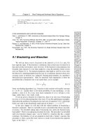
Figure 1—
This control unit finite state machine schematic implements
the symbol CTRLFSM in Figure 2. It consists of the memory cycle FSM
(see Figure 4), plus instruction annulment and pending request registers.
The FSM outputs are derived from the machines current and next states.
a)
b)
4
Issue 117 April 2000 CIRCUIT CELLAR
®
www.circuitcellar.com
DMAREQ has been asserted, you
insert one DMA memory cycle.
This PC register file costs eight
CLBs for the RAM, but saves 16 CLBs
(otherwise necessary for a separate 16-
bit DMA address counter and a 16-bit
2-1 address mux), and shaves a couple
of nanoseconds from the system’s
critical path. It’s a nice example of a
problem-specific optimization you
can build with a customizable
processor.
To recap, each instruction takes
three pipeline cycles to move through
the instruction fetch, operand fetch
and decode, and execute pipeline
stages. Each pipeline cycle requires up
to three memory access cycles
(mandatory instruction fetch, optional
DMA, and optional EX stage load or
store). Each memory access cycle
requires one or more clock cycles.
CONTROL UNIT DESIGN
Now that you understand the pipe-
line, you are ready to design the con-
trol unit. (For more information on
RISC pipelines, see Computer Orga-
nization and Design: The Hardware/
Software Interface, by Patterson and
Hennessy.) [1] First, some important
naming conventions. Some control
unit signal names have prefixes and
suffixes to recognize their function or
context (most signal names sans pre-
fix are DC stage signals):
• Nsig: not signal—signal inverted
• DCsig: a DC stage signal
• EXsig: an EX stage signal
• sigN: signal in “next cycle”—input
to a flip-flop whose output is sig
• sigCE: flip-flop clock enable
• sigT: active low 3-state buffer
output enable
Each instruction flows through the
three stages (IF, DC, and EX) of the
control unit (see Figure 2) pipeline. In
the IF stage, when the instruction
fetch read completes, the new instruc-
tion at INSN
15:0
is latched into IR.
In the DC stage, DECODE decodes
IR to derive internal control signals.
In the first half clock cycle, CTRL
drives RNA
3:0
and RNB
3:0
with the
source registers to read, and drives
FWD and IMM
5:0
to select the A and B
operands. If the instruction is a
branch, CTRL determines if it is
taken. Then as the pipeline advances,
the instruction passes into EXIR.
In the EX stage, CTRL drives ALU
and result mux controls. If the in-
Table 4—
RNA and RNB control the A and B ports of
the register file. While CLK is high, they select which
registers to read, based upon register fields of the
instruction in the DC stage. While CLK is low, they
select which register to write, based upon the instruc-
tion in the EX stage.
RNA When
RA DC: add sub addi
lw lb sw sb jal
RD DC:
all rr, ri format
0 DC: call
EXRD EX:
all but call
15 EX: call
RNB When
RB DC: add sub,
all rr fmt
RD DC: sw sb
EXRD EX:
all but call
15 EX: call
FD16CE
NEXTIR
D[15:0]
CE
C
Q[15:0]
CLR
^
CLK
IF
A[15:0]
O[15:0]
B[15:0]
SEL
INT
NIR[15:0]
INSN[15:0]
IRMUX
IRMUX
IF
IFINT
IRMUX[15:0]
D[15:0]
CE
C
^
PCE
CLK
CLR
Q[15:0]
FD16CE
IR
EXIR
FD16CE
D[15:0]
IR[15:0]
CE
C
^
CLK
PCE
CLR
Q[15:0]
EXIRB
I[15:0]
O[15:0]
EXIR[15:0]
I[15:0] O[15:0]
IRB
IMMB
I[15:0] O[15:0]
BUF16
OP[3:0],RD[3:0],RA[3:0],RB[3:0]
IR[11:0]
BUF16
IMM[11:0]
BUF16
EXOP[3:0],EXRD[3:0],BRDISP[7:0]
BRDISP[7:0]
Instruction registers
FSM
CTRLFSM
PCE
ACE
WORDN
READN
DBUSN
IF
IFINT
DMA
EXAN
EXANNUL
SELPC
ZEROPC
DMAPC
PCCE
RETCE
PCE
ACE
WORDN
READN
DBUSN
IF
IFINT
DMA
EXAN
EXANNUL
SELPC
ZEROPC
DMAPC
PCCE
RETCE
IREQ
DCINTINH
EXLDST
EXLBSB
EXST
BRANCH
JUMP
ZERODMA
DMAREQ
RDY
CLK
IREQ
DCINTINH
EXLDST
EXLBSB
EXST
BRANCH
JUMP
ZERODMA
DMAREQ
RDY
CLK
RRRI
IMM_12
IMM_4
SEXTIMM4
WORDIMM4
ADDSUB
SUB
ST
CALL
NSUM
NLOGIC
NLW
NLD
NLB
NSR
NSL
NJAL
BR
ADCSBC
NSUB
DCINTINH
EXNSUB
EXFNSRA
EXIMM
EXLDST
EXLBSB
EXRESULTS
EXCALL
EXJAL
RRRI
IMM12
IMM4
SEXTIMM4
WORDIMM4
ADDSUB
SUB
ST
CALL
NSUM
NLOGIC
NLW
NLD
NLB
NSR
NSL
NJAL
BR
ADCSBC
NSUB
DCINTINH
EXNSUB
EXFNSRA
EXIMM
EXLDST
EXLBSB
EXRESULTS
EXJALI
EXJAL
OP[3:0]
FN[3:0]
EXOP[3:0]
PCE
CLK
EXOP[3:0]
OP[3:0]
IR[7:4]
DECODE
Instruction decoder
PCE
CLK
Control state machine
^
^
Figure 2—
This control unit schematic implements
half of the symbol CTRL16 in last month’s Figure 2,
including the CPU finite state machine, instruction
register pipline, and instruction decoder. Instructions
enter on INSN
15:0
and are latched in IR and decoded.
CIRCUIT CELLAR
®
Issue 117 April 2000
5
www.circuitcellar.com
• RDY: memory cycle complete (input
from the memory controller)
• READN: next memory cycle is a
read transaction—true except for
stores
• WORDN: next cycle is 16-bit data—
true except for byte loads/stores
• DBUSN: next cycle is a load/store,
and it needs the on-chip data bus
• ACE (address clock enable): the next
address AN
15:0
(a datapath output)
and the above control outputs are
all valid, so start a new memory
transaction in the next clock cycle.
ACE equals RDY, because if
memory is ready, the CPU is
always eager to start another
memory transaction.
There are no IF stage control out-
puts. Internal to the control unit,
three signals control IF stage re-
sources. Those three signals are:
• PCE: enable IR and EXIR
clocking
• IF: asserted in an instruction
fetch memory cycle
• IFINT: force the next instruction to
be int = jalr14,10(r0) =
Table 5—
Here’s a look at the result multiplexer output enable controls.
The instruction determines which enable is asserted and which function
unit drives RESULT
15:0
.
Enable Instruction Source
SUMT add sub addi SUM
15:0
adc sbc adci sbci
LOGICT and or xor andn LOGIC
15:0
andi ori xori andni
SLT slli A
14:0
|| 0
SRT srli srai SRI || A
15:1
ZXT lb 0
15:8
RETADT jal call RETAD
15:0
none
sw sb br* imm —
0xAE01
If a DMA or load/store access
is pending, IF enables NEXTIR to
capture the previously fetched
instruction (take a look back at
time t
3
in Table 3). Otherwise,
the instruction fetch is the only
memory access in the pipe stage.
So, IF is then asserted with PCE,
and IRMUX selects the INSN
15:0
input as the next instruction to
complete.
DECODE STAGE
The greater part of the control unit
operates in the DC stage. It must
decode the new instruction, control
the register file, the A and B operand
multiplexers, and prepare most EX
stage control signals.
The instruction register IR latches
the new instruction word as the DC
stage begins. The buffers IRB and
IMMB break out the instruction fields
OP, RD, and so forth—IR
15:12
is re-
named OP
3:0
and so on (the tools opti-
mize away these buffers).
The instruction decoder DECODE
is simple. It is a set of 30 ROM 16x1s,
gate expressions, and a handful of flip-
flops. Each ROM inputs OP
3:0
or
EXOP
3:0
and outputs some decoded
signal. The decoder is relatively
compact because xr16 has a simple
instruction set, and its 4-bit opcodes
are a good match for the FPGA’s 4
LUTs.
The register file control signals,
shared by both the DC and EX stages,
are RNA
3:0
: port A register number;
RNB
3:0
: port B register number; and
RFWE: register file write enable.
struction is a load/store, it in-
serts a memory access. In the last
half cycle, RNA and RNB both
drive the destination register
number to store the result into
the register file.
Let’s consider each part of the
control finite state machine (see
Fig
ure 1).
The control FSM has
three states:
• IF: current memory access is an
instruction fetch cycle
• DMA: current access is a DMA
cycle
• LS: current access is a load/store
Figure 4 shows the state transition
diagram. The FSM clocks when one
memory transaction completes and
another begins (on RDY). CTRLFSM
also has several other bits of state:
• DCANNUL: annul DC stage
• EXANNUL: annul EX stage
• DCINT: int in DC stage
• DMAP: DMA transfer pending
• INTP: interrupt pending
DCANNUL and EXANNUL are set
after executing a jump or taken
branch. They suppress any effects of
the two instructions in the branch
shadow, including register file write-
back and load/store memory accesses.
So, an annulled add still fetches and
adds its operands, but its results are
not retired to the register file.
DCINT is set in the pipeline cycle
following the insertion of the int
instruction. It inhibits clocking of
RET for one cycle, so that the int
picks up the return address of the
interrupted instruction rather than
the instruction after that.
The highest fan-out control signal is
PCE, the pipeline clock enable. Most
datapath registers are enabled by PCE.
It indicates that all pipe stages are
ready and the pipeline can advance.
PCE is asserted when RDY signals
completion of the last memory cycle
in the current pipeline cycle. If mem-
ory isn’t ready, PCE isn’t asserted, and
the pipeline stalls for one cycle.
The control FSM also takes care of
managing the memory interface via
the following signals:
Table 6—
Here’s a look at the result multiplexer output enable controls. The instruction determines which enable to
assert and thus determines which function unit drives the RESULT bus.
Next cycle Next address Outputs
IF AN ← PC
0
+= 2 SELPC PCCE
IF
branch
AN ← PC
0
+= 2×disp8 BRANCH SELPC PCCE
IF
jal call
AN ← PC
0
= SUM PCCE
IF
reset
AN ← PC
0
= 0 SELPC ZEROPC PCCE
LS
load/store
AN ← SUM —
DMA AN ← PC
1
+= 2 SELPC DMAPC PCCE
DMA
reset
AN ← PC
1
= 0 SELPC ZEROPC DMAPC PCCE
6
Issue 117 April 2000 CIRCUIT CELLAR
®
www.circuitcellar.com
RNA
RA[3:0]
RD[3:0]
SELRD
SELR0
EXRD[3:0]
SELR15
SELSRC
RA[3:0]
RD[3:0]
RRRI
CALL
EXRD[3:0]
EXCALL
CLK
RN[3:0]
FWD
RZERO
EXRESULTS
EXANNUL
RZERO
RNA[3:0]
AND3B1
FWD
RNMUX4
RLOC=R2C0
RA[3:0]
RD[3:0]
SELRD
SELR0
EXRD[3:0]
SELR15
SELSRC
RN[3:0]
FWD
RZERO
RNB[3:0]
"N.C."
"N.C."
RB[3:0]
RD[3:0]
ST
GND
EXRD[3:0]
EXCALL
CLK
RNMUX4
RLOC=R2C1
RNB
IR3
SEXTIMM4
IMM_12
IR0
WORDIMM4
IMMOP[5:0]
IMMOP0
IMMOP1
BUF
BUF
BUF
IMMOP2
IMMOP3
IMMOP4
IMM_4
IMM_4
IMM_12
IR0
WORDMM4
PCE
IMMOP5
BCE15_4
EXIMM
EXANNUL
Z
N
C
V
COND[3:0]
TRUE
IR[11:8]
Z
N
CO
V
TRUE
BR
EXAN
TRUTH
BRN
PCE
CLK
CLR
CE
D
C
BRANCH
FDCE
Q
TRUE
DC:conditional branches
DMAPC
BRANCH
EXANNUL
EXJAL
JUMP
D0 Q0
D1 Q1
D2 Q2
D3 Q3
CE
CLK
NLB
NSR
NSL
NJAL
PCE
CLK
ZXT
SRT
SLT
RETARDT
FD4PE
INIT= S
D0 Q0
D1 Q1
D2 Q2
D3 Q3
CE
CLK
NSUM
NLOGIC
NLW
NLD
PCE
CLK
SUMT
LOGICT
"N.C."
"N.C."
FD4PE
INIT= S
T2
T1
SRI
BUF
BUF
BUF
EXFNSRA
A15
SRI
EXIR4
EXIR5
LOGICOP0
LOGICOP1
LOGICOP[1:0]
EXNSUB ADD
D Q
CE
C
CLR
PCE
CLK
CI
FDCE
CI
CO
ADCSBC
NSUB
^
EXRESULTS
PCE
EXANNUL
RZERO
DC: operand selection
Execute stage
RFWE
^^
Figure 3—
The remainder of the control unit schematic implements the DC stage operand selection
logic including register file, immediate operand control, branch logic, EX stage ALU, and result mux
controls.
With CLK high,
CTRL drives RNA
and RNB with the
DC stage
instruction’s source
register numbers.
With CLK low,
CTRL drives RNA
and RNB with the
EX stage destination
register number.
RFWE is asserted
with PCE when
there is a result to
write back. It is false
for instructions,
which produces no
result (immediate
prefix, branch, or
store) for annulled
instructions, and for
destination r0.
The muxes RNA
and RNB produce
RNA
3:0
and RNB
3:0
, as
shown in Table 4,
as
selected by decode
outputs RRRI,
CALL, ST, EXCALL,
and CLK. Call is
irregular. It
computes r15 = pc,
pc = r0 + imm12<<4,
and the registers r15
and r0 are implicit.
The FWD signal
causes RESULT to be
forwarded into A,
overriding AREG.
CTRL asserts FWD when the EX stage
destination register equals the DC
stage source register A (detected
within RNA), unless the EX stage
instruction is annulled or its
destination is r0.
Last month, I discussed IMMED,
the BREG/immediate operand mux.
IMMOP
5:0
controls IMMED, based
upon the decoder outputs
WORDIMM, SEXTIMM4, IMM_12,
and IMM_4.
B
3:0
is clock enabled on PCE, but
B
15:4
uses B15_4CE. B15_4CE is PCE,
unless the EX stage instruction is
imm. Thus, the imm prefix establishes
B
15:4
, and the subsequent immediate
operand instruction provides B
3:0
only.
Now, turning to conditional
branches, if the DC stage instruction
is a branch, then the EX stage
instruction must be add, sub, or
addi, which drives the control unit’s
condition inputs Z (zero), N
(negative), CO (carry-out), and V
(overflow).
Late in the DC stage, the TRUE
macro evaluates whether or not the
branch condition COND is true with
respect to the condition inputs. If so,
and if the branch instruction is not
annulled, the BRANCH flip-flop is
set. Therefore, as the pipeline
advances and the branch instruction
enters the EX stage, the BRANCH
control output is asserted. This
directs PCINCR to take the branch
by adding 2×disp8 to
the PC.
THE EXECUTE
STAGE
Now, let’s discuss
the EX stage ALU,
result mux, and
address unit controls.
The ALU and shift
control outputs are:
• ADD: set unless the
instruction is sub or
sbc
• CI: carry-in. 0 for
add and 1 for sub,
unless it’s adc or sbc
where we XOR in the
previous carry-out
• LOGICOP
1:0
: select
and, or, xor, or andn.
LOGICOP
1:0
is simply
EXIR
5:4
(i.e., EX stage
copy of FN
1:0
)
• SRI: shift right
input—0 for srli and
A
15
for srai (shift
right arithmetic)
slxi and srxi (shift
extended left/right for
multi-word shift sup-
port) are not yet imple-
mented. Be my guest!
The result mux
control outputs SUMT,
LOGICT, SLT, SRT,
SXT, and RETADT are
active low RESULT bus 3-state output
enables. Each cycle, all EX stage
function units produce results. One
asserted T enables its unit’s 3-state
buffers to drive the RESULT bus, as
shown in Table 5.
ZXT zeroes RESULT
15:8
during lb.
As you’ll see next month, the system
drives RESULT
7:0
with the byte load
result.
The following outputs control the
address unit:
• BRANCH: if set, add 2×disp8 to PC,
otherwise add +2
• SELPC: if set, next address is
PCNEXT
15:0
, otherwise SUM
15:0
• ZEROPC: if set, next address is 0
• PCCE (PC clock enable): update PC
i
CIRCUIT CELLAR
®
Issue 117 April 2000
7
www.circuitcellar.com
Jan Gray is a software developer
whose products include a leading C++
compiler. He has been building FPGA
processors and systems since 1994,
and he now designs for Gray Re-
search LLC. You may reach him at
SOFTWARE
Visit the Circuit Cellar web site
for more information, including
specifications, source code,
schematics, and links to related
sites.
REFERENCE
[1] D. Patterson and J. Hennessy,
Computer Organization and
Design: The Hardware/Software
Interface, Morgan Kaufmann, San
Mateo, CA, 1994.
Figure 4
—Each memory cycle is an instruction fetch
unless there is a DMA transfer pending or the EX stage
instruction is a load or store. The FSM clocks when one
memory transaction completes and another begins (on
RDY).
IF
DMA
LS
L
S
P
*
L
S
P
D
M
A
P
*
D
M
A
P
×
L
S
P
*
D
M
A
P
×
L
S
P
DMAP: DMA pending
LSP: load/store pending
• DMAPC: if set, fetch and update
PC
1
(DMA address), otherwise PC
0
(PC)
Depending on the next memory
cycle and the current EX stage
instruction, the control unit selects
the next address by asserting certain
combinations of control outputs (see
Table 6).
WRAP-UP
This month, we considered pipe-
lined processor design issues and ex-
plored the detailed implementation of
our xr16 control unit—and lived! The
CPU design is complete. The final
article in this series tackles the design
of this System-on-a-Chip. I
© Circuit Cellar, The Magazine for Computer Applications.
Reprinted with permission. For subscription information call
(860) 875-2199, email or on our
web site at www.circuitcellar.com.