Tài liệu Báo cáo " Research on optimal silicon etching condition in TMAH solution and application for MEMS structure fabrication " ppt
Bạn đang xem bản rút gọn của tài liệu. Xem và tải ngay bản đầy đủ của tài liệu tại đây (108.94 KB, 7 trang )
VNU Journal of Science, Mathematics - Physics 25 (2009) 161-167
161
Research on optimal silicon etching condition in TMAH
solution and application for MEMS structure fabrication
Dinh Van Dung*
Hanoi Pedagogical University No.2, Hanoi, Vietnam
Received 15 May 2009
Abstract. The research of optimal condition for etching silicon in TMAH solution with controlled
etch rate and low surface roughness is the purpose of this study. The investigation on the influence
of temperature, agitation, size of etch-window, etch time on etch rate and the surface roughness
were carried out. With the TMAH concentration of 20% in weight, the optimal etching conditions
were as follows: temperature of about 80 – 90
o
C, agitation of 150 - 200 rpm. The etch rate is
controlled in range of 0.49 – 0.72 µm/min. The etched surface roughness was lower than 70 nm.
Development of TMAH application, a useful procedure for fabricating MEMS structures
(piezoresistive accelerometer) was suggested.
Keywords: MEMS technology, TMAH, silicon etching, accelerometer, MEMS fabrication.
1. Introduction
Anisotropic etching of silicon is a key technology for fabricating various 3-dimensional structures
for Micro Electro Mechanical Systems (MEMS). Although deep reactive ion etching (Deep RIE) has
become popular for realizing high aspect ratio silicon microstructures, the advantages of silicon
anisotropic etching technology such as low process cost, better surface smoothness and lower
environmental pollution makes them as a complementally technology.
The most popular chemical etchants are Potassium Hydroxide KOH and Tetra Methyl Ammonium
Hydroxide (CH
3
)
4
NOH (TMAH). KOH was proposed for application very early. The salient good
points of this etchant are its possibility of making structures with high aspect ratio because of the
strong anisotropy in etch rate. However, the drawback of KOH is its incompatibility with the IC
technology [1]. To overcome the disadvantages of KOH, Tetra Methyl Ammonium Hydroxide
(TMAH) was later introduced as a fruitful solution for MEMS fabrication [2].
TMAH is a weak organic hydroxide without any metal ions, so it is quite compatible with the IC
technology. The chemical product is nontoxic and easy in handle [3,4]. Compared to etching in KOH
solution, SiO
2
and Si
3
N
4
are better mask materials for etching processes in TMAH. Especially, the
studies of Tabata [4-6] show that, the Al etching in TMAH solution can be decreased to extremely low
etch rate when some appropriate amount of silicon is diluted into the TMAH solution. The presence of
integrated circuits as well as Al interconnections is obvious in MEMS fabrications. If the adequate
etching condition of which the solution is assumed not to etch Al is found, then the problem of Al
______
*
E-mail:
D.V. Dung / VNU Journal of Science, Mathematics - Physics 25 (2009) 161-167
162
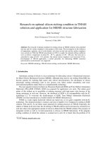
Fig. 1. The etching system of Model 5000.
connections protection and integrated circuits protection in silicon etching process can seem to be
solved. Thus, the use of TMAH as the etchant seems to be optimal in the case when only a one-side
aligner is available and the thermal SiO
2
is used as the mask material. The point will be especially
useful for MEMS devices fabricated by etching through whole silicon wafer such as beam structures
in accelerometers, gyroscopes… Some papers reported that, the TMAH solution with the
concentrations higher than 20 wt. % allows fabricating smooth surfaces [6,7]. The silicon etch rate and
the smoothness of etched surface can be improved considerably by controlling the conditions of
etching process.
In this study, the influences of temperature, agitation, etch time, size of etch-windows on the etch
rate and etched surface roughness were carried out. Based on the obtained results, the optimal
conditions for etching silicon in TMAH were suggested. Finally, a useful procedure for fabricating
MEMS structure using beams as mechanical element (for example: MEMS piezoresistive
accelerometer) with the TMAH etchant was presented.
2. Experiments
In order to maintain the concentration and
temperature of TMAH solution as well as the
agitation at controlled speed during etching
process, a special etching system IKA-WERKE
MODEL 5000 was used (Fig. 1). The system
consists of a thermostat which allows heating
and maintaining temperature of the solution in
the range of room temperature to 250
0
C and a
magnetic stirrer with controlled speed of 0 –
650 round per minute (rpm). The TMAH
solution is contained in a vessel of 5-liter
volume covered by a double-wall lid. A cool
water flow running through the lid can make
chemical product vapor condensed during the
etching process in order to maintain the
constant concentration of solution.
Silicon wafers of 2-inch, (100) orientation,
n-type, and polished double side, phosphorous
doped with sensitivities of 1 - 20 Ω.cm, 260 ±
25 µm thickness were used for experiments.
The protection material was only SiO
2
layer
formed on two sides of silicon wafer by wet
thermal oxidation. In the oxidation condition of
1100
0
C, wet oxygen 1.5 l/min flow, oxidation
time 3 hours, the thickness of the oxide layer was about 1.1 µm. The oxide layer is sufficient to protect
the samples during etching time including the case of etching through whole wafer thickness. Etch-
widows were formed by photolithography technique. In the investigations on influence of temperature,
stirring and etch time, the size of etch-window were chosen at 1 x 1 mm
2
. For the studies on influence
of etch-window size, the etch-window was chosen with the edge size of 1, 2, 4, 6, and 8 mm.
D.V. Dung / VNU Journal of Science, Mathematics - Physics 25 (2009) 161-167
163
The average etch rate was calculated by dividing the etched groove height by etch time. Here, the
etch height was measured by the instrument of Interferometric Optical Profilometer LEICA DMRM
with very high accuracy. The profile of etched surface can also be measured by using this instrument.
The process program of M3D connected to computer allows calculating average arithmetic roughness
Ra and peak roughness Rt (distance from the lowest point to the highest point on the etched surface).
They are important quantities determining the etched surface quality in MEMS fabrications.
3. Results and discussion
The Figs 2 and 3 show the results on the influence of temperature on etch rate and etched surface
roughness. The experimental conditions were chosen as follows: TMAH 20% in weight, agitation of
150 rpm, etch time of 30 minutes.
1
10
100
2,7 2,8 2,9 3 3,1 3,2
Etching in TMAH 20%
y = 1,6745e+09 * e^(-6,3481x) R= 0,99328
Etch-rate (µm/h)
1/T (10
-3
K
-1
)
Fig. 2. The influence of temperature on etch rate.
Etching in TMAH 20%
0
200
400
600
800
1000
1200
1400
50 60 70 80 90
Temperature (°C)
Roughness (nm)
Ra
Rt
Fig. 3. The influence of temperature on surface
roughness.
The etch-rate increases strongly with increasing temperature. The fit curve has a shape of an
exponential curve. The small deviation of experimental points compared to the fit curve shows that the
obtained result corresponds to the theoretical rule. The activation energy is calculated E
a
= 0.548 eV
which is in good agreement with the result of Tabata [5].
At around 60°C, the etched-surface (100) is the roughest. At about 50°C, the average surface
roughness is much lower than at 60°C. At these low temperatures, the intersection between wall side
(111) and bottom side (100) is unclear. There are many pyramids on the bottom surface (100). At
70°C, the etch-rate is significantly higher and the intersection between (111 and (100) planes is clear,
the etched surface (100) is smoother. However, there are still some peaks on the surface and the
average roughness is still high.
At high temperatures of 80°C and 90°C, the etch process occurs very fast. On the etched surface
(100), no pyramids were observed. The intersection between (111) plane and (100) plane was very
clear; the surface smoothness was very good. Although the etch-rate at 80°C was not as high as at
90°C, but the surface quality in the condition of 80°C was better.
D.V. Dung / VNU Journal of Science, Mathematics - Physics 25 (2009) 161-167
164
Etching in TMAH 20%
15
17
19
21
23
25
27
29
0 100 150 200 250
Agitation (rpm)
Etch-rate (µm/h)
Fig. 4. The influence of agitation on etch rate.
Etching in TMAH 20%
0
5
10
15
20
25
30
0 100 150 200 250
Agitation (rpm)
Roughness Ra (nm)
Fig. 5. The influence of agitation on surface
roughness.
In the Figs of 4 and 5, the results on the influence of agitation are shown. The experiments were
done in the TMAH solution of 20% in weight at temperature of 80°C. The stirring has a good action
on the etched product transportation from etched-surface into the solution and fresh solution to the
etched surface. So it makes etch process faster. But the agitation at very low speed or very high speed
can make opposite effects. The stirring speed of 150 rpm is optimal for all Ra and Rt roughness. The
etch-rate has largest value when the solution was stirred at about 150 rpm.
The influences of the size of etch-window on etch rate and surface roughness are presented in Figs
6 and 7. The etch conditions were the following: the agitation of 150 rpm, 30 minutes, temperature
80°C, TMAH 20% in weight. There is a light difference in etch-rate at different sizes of etch-window.
The difference was caused by many reasons such as the position of the wafer and the holder in the
solution, the declination of surface (100) compared to horizon plane…The surface roughness has also
difference but not much when the size of etch-window changes. With the etch-window larger than 1 x
1 mm
2
, no rule of the influence was found in the cases.
Etching in TMAH 20%
0
5
10
15
20
25
30
1 2 4 6 8
The size of etch-window (mm2)
Etch-rate (µm/h)
Fig. 6. The influence of size of etch-window on etch-
rate.
Etching in TMAH 20%
0
50
100
150
200
250
300
1 2 4 6 8
The size of etch-window (mm2)
Roughness (nm)
Ra
Rt
Fig. 7. The influence of size of etch-window on surface
roughness.
D.V. Dung / VNU Journal of Science, Mathematics - Physics 25 (2009) 161-167
165
Finally, the results on the influence of etch time on etch rate and roughness are reported. The
experimental conditions were chosen as temperature 80°C, 150 rpm, TMAH 20% in weight. With
increasing etch time, the etched groove depth increases. The transportation process of etched products
from the etch-surface into solution and fresh solution to silicon surface becomes more difficult. This
makes the average etch-rate to decrease lightly with time. Whereas, the amount and the height of
pyramids will increase when increasing etch-time. That is the explanations for the results in Fig.8 and
Fig.9.
Etching in TMAH 20%
0
0.1
0.2
0.3
0.4
0.5
0.6
30 60 90 120 150
Time (min)
Average etch-rate (µm/min)
Fig. 8. The dependency of average etch-rate on time.
Etching in TMAH 20%
0
10
20
30
40
50
60
70
80
90
100
30 60 90 120 150
Time (min)
Ruoghness Ra (nm)
Fig. 9. The influence of etch time on surface roughness.
A good etched surface was obtained in the etching condition of TMAH 20 wt.%, temperature
80
0
C, and 150-rpm agitation as shown by SEM picture in Fig. 10. The etched surface (100) was very
smooth with Ra = 12 nm, Rt = 63 nm.
4. TMAH application for MEMS structure fabrication
Al is etched in TMAH solution, but the etch rate decreases very sharply when the suitable amount
of silicon was dissolved into the solution (Fig 11) [6]. The etch rate can be lower than 0.001 µm/min if
the amount of 3.5 silicon mol is dissolved into the TMAH 22 wt. % solution.
In MEMS fabrications, especially for the structures using piezoresistive effect, the electrical part
of sensor including Al interconnections and integrated circuits is usually integrated on one chip, so the
protection of the electrical structures is very important in etching process for forming structure.
D.V. Dung / VNU Journal of Science, Mathematics - Physics 25 (2009) 161-167
166
Fig. 10. SEM picture of etched surface in TMAH 20
wt. %, 80
0
C, 150 rpm.
Fig. 11. The dependence of Al etch rate on diluted
silicon amount in the TMAH 22wt.% solution [4].
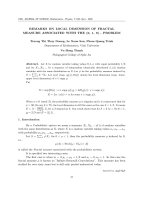
Fig. 12. Fabrication procedure of MEMS piezoresistive accelerometer using TMAH.
Silicon wafer: standard cleaning
Pattern aligner marks
Etching for aligner marks
Pattern etch window from back side
Oxidation
Etching from back side
Pattern resistor
Diffusion
Pattern etch window from front side
Al Evaporation
Pattern contact
Etch from front side
Encapsulation
Pattern contact
D.V. Dung / VNU Journal of Science, Mathematics - Physics 25 (2009) 161-167
167
Based on the low Al etching in TMAH, a useful suggestion for fabricating MEMS using beam
structure as mechanical sensitive element such as in piezoresistive accelerometer was given in Fig 12.
In the procedure, we use only the photolithography instrument of one side aligner. The aligner marks
for locating position precisely from two sides of the wafer are formed by etching through whole the
wafer thickness. The protection material during etching process is only SiO
2
making by simply
thermal oxidation. The first steps are carried out to make aligner marks; next the steps of making
membrane and mesa mass are done. The electrical part is fabricated before releasing the beam
structure in order to work easily lithography process. Then, the step of releasing beam structure by
etching through whole the wafer is done without making Al protection layer in solution.
5. Conclusions
The obtained results show that, it is quite possible to control etch rate and lower etched surface
roughness by controlling temperature and agitation suitably. In the TMAH solution of 20 % in weight,
the optimized silicon etching condition in which the silicon etch rate is high and the etched surface
roughness is low are as follows: temperature of 80 – 90
0
C, agitation of about 150 – 200 rpm. When the
solution temperature increases from 80 to 90
0
C, the etch rate increases considerably from 0.49
µm/min to 0.72 µm/min. At about 150-rpm stirring, the average arithmetic roughness is lower than 70
nm. For the MEMS structures with thickness larger than 5 µm, the surface roughness lower than 70
nm is quite acceptable.
The Al etching at low etch-rate in TMAH makes the protection of electrical part in etching process
to become much easier. For the technology condition in which a one-side aligner is available and the
thermal SiO
2
is used as the mask material, aligner marks for locating precisely position from two sides
of wafer were form by etching through whole the wafer thickness, the use of TMAH as the etchant
seems to be technology solution allows being successful in fabrication of complex MEMS structures,
especially beam structure such as in accelerometer, gyroscope… The suggested solution for
accelerometer fabrication is quite possible to carry out in the technology condition in ITIMS
laboratory.
Acknowledgement. This research was carried out in Institute of Electronics Fundamental (IEF),
University of South Paris, France and International Training Institute for Materials Science (ITIMS),
Hanoi University of Technology, Vietnam.
References
[1] H.R.Huff, R.R.Burgess, Semiconductor Silicon (1973).
[2] M. Asano, T. Cho, H. Muraoka, Electrochem. Soc. Ext. Abstr. (1976) 354.
[3] O. Tabata, R. Asahi, H. Funabashi, S. Sugiyama, Tec. Dig. of Int. Conf. On Solid-State Sensors and Actuators (1991)
811.
[4] O. Tabata, R.Asahi, H. Funabashi, K. Shimakao, S. Sugiyama, Sensors and Actuators A 34 (1992) 51.
[5] O. Tabata, M. Yashima, T. Yoshioka, K. Sato, The 10th Int. Conf. On Solid-State Sensors and Actuators (1999) 542.
[6] O. Tabata, Sensors and Materials Vol. 13, No. 5 (2001) 271.
[7] J. van Suchtelen, K. Sato, E. van Veenendaal, A.J. Nijdam, J.G.E. Gardeniers, W.J.P. van Enckevort, M. Elwenspoek,
Proceedings of the IEEE Micro Electro Mechanical Systems (1999) 332.