vi mạch điện tử
Bạn đang xem bản rút gọn của tài liệu. Xem và tải ngay bản đầy đủ của tài liệu tại đây (240.26 KB, 15 trang )
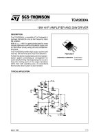
TDA2030A
18W Hi-Fi AMPLIFIER AND 35W DRIVER
March 1995
PENTAWATT
ORDERING NUMBERS : TDA2030AH
TDA2030AV
DESCRIPTION
The TDA2030A is a monolithic IC in Pentawatt
package intended for use as low frequency class
AB amplifier.
With V
S max
= 44V it is particularly suited for more
reliable applications without regulated supply and
for 35W driver circuits using low-cost complemen-
tary pairs.
The TDA2030A provides high output current and
has very low harmonic and cross-over distortion.
Further the device incorporates a short circuit pro-
tection system comprising an arrangement for
automaticallylimiting the dissipated power so as to
keep the working point of the output transistors
within their safe operating area. A conventional
thermal shut-down system is also included.
TYPICAL APPLICATION
1/15
TEST CIRCUIT
PIN CONNECTION (Top view)
THERMAL DATA
Symbol Parameter Value Unit
R
th (j-case)
Thermal Resistance Junction-case Max 3
°C/W
TDA2030A
2/15
ABSOLUTE MAXIMUM RATINGS
Symbol Parameter Value Unit
V
s
Supply Voltage
± 22
V
V
i
Input Voltage V
s
V
i
Differential Input Voltage
± 15
V
I
o
Peak Output Current (internally limited) 3.5 A
P
tot
Total Power Dissipation at T
case
=90°C
20 W
T
stg
,T
j
Storage and Junction Temperature – 40 to + 150 °
C
ELECTRICAL CHARACTERISTICS
(Refer to the test circuit, V
S
= ± 16V, T
amb
=25
o
C unless otherwise specified)
Symbol Parameter Test Conditions Min. Typ. Max. Unit
V
s
Supply Voltage
± 6 ± 22
V
I
d
Quiescent Drain Current 50 80 mA
I
b
Input Bias Current
V
S
= ± 22V
0.2 2
µA
V
os
Input Offset Voltage
V
S
= ± 22V ± 2 ± 20
mV
I
os
Input Offset Current ±
20 ± 200
nA
P
O
Output Power d = 0.5%, G
v
= 26dB
f = 40 to 15000Hz
R
L
=4Ω
R
L
=8Ω
V
S
=±19V R
L
=8Ω
15
10
13
18
12
16
W
BW Power Bandwidth
P
o
= 15W R
L
=4Ω 100 kHz
SR Slew Rate 8
V/µsec
G
v
Open Loop Voltage Gain f = 1kHz 80 dB
G
v
Closed Loop Voltage Gain f = 1kHz 25.5 26 26.5 dB
d Total Harmonic Distortion
P
o
= 0.1 to 14W R
L
=4Ω
f = 40 to 15 000Hz f = 1kHz
P
o
= 0.1 to 9W, f = 40 to 15 000Hz
R
L
=8Ω
0.08
0.03
0.5
%
%
%
d
2
Second Order CCIF Intermodulation
Distortion
P
O
= 4W, f
2
–f
1
= 1kHz, R
L
=4Ω 0.03 %
d
3
Third Order CCIF Intermodulation
Distortion
f
1
= 14kHz, f
2
= 15kHz
2f
1
–f
2
= 13kHz
0.08 %
e
N
Input Noise Voltage B = Curve A
B = 22Hz to 22kHz
2
310
µV
µV
i
N
Input Noise Current B = Curve A
B = 22Hz to 22kHz
50
80 200
pA
pA
S/N Signal to Noise Ratio
R
L
=4Ω,R
g
= 10kΩ, B = Curve A
P
O
= 15W
P
O
=1W
106
94
dB
dB
R
i
Input Resistance (pin 1) (open loop) f = 1kHz 0.5 5
MΩ
SVR Supply Voltage Rejection
R
L
=4Ω,R
g
= 22kΩ
G
v
= 26dB, f = 100 Hz
54 dB
T
j
Thermal Shut-down Junction
Temperature
145 °C
TDA2030A
3/15
Figure 3 : Output Power versus Supply Voltage
Figure 4 : Total Harmonic Distortion versus
Output Power (test using rise filters)
Figure 1 : Single Supply Amplifier
Figure 2 : Open Loop-frequency Response
Figure 5 : Two Tone CCIF Intremodulation
Distortion
TDA2030A
4/15
Figure 6 : Large Signal Frequency Response Figure 7 : Maximum Allowable Power Dissipation
versus Ambient Temperature
Figure 10 : Output Power versus Input Level Figure 11 : Power Dissipation versus Output
Power
Figure 8 : Output Power versus Supply Voltage
Figure 9 : Total Harmonic Distortion versus
Output Power
TDA2030A
5/15
Figure 12 : Single Supply High Power Amplifier (TDA2030A+ BD907/BD908)
Figure 13 : P.C. Board and Component Layout for the Circuit of Figure 12 (1:1 scale)
TDA2030A
6/15
TYPICAL PERFORMANCE OF THE CIRCUIT OF FIGURE 12
Symbol Parameter Test Conditions Min. Typ. Max. Unit
V
s
Supply Voltage 36 44 V
I
d
Quiescent Drain Current V
s
= 36V 50 mA
P
o
Output Power
d = 0.5%, R
L
=4Ω, f = 40 z to 15Hz
V
s
= 39V
V
s
= 36V
d = 10%, R
L
=4Ω, f = 1kHz
V
s
= 39V
V
s
= 36V
35
28
44
35
W
W
W
W
G
v
Voltage Gain f = 1kHz 19.5 20 20.5 dB
SR Slew Rate 8
V/µsec
d Total Harmonic Distortion f = 1kHz
P
o
= 20W f = 40Hz to 15kHz
0.02
0.05
%
%
V
i
Input Sensitivity
G
v
= 20dB, f = 1kHz, P
o
= 20W, R
L
=4Ω 890 mV
S/N Signal to Noise Ratio
R
L
=4Ω,R
g
= 10kΩ, B = Curve A
P
o
= 25W
P
o
=4W
108
100
dB
Figure 14 : Typical Amplifier with Spilt Power Supply
Figure 15 : P.C. Board and Component Layout for the Circuit of Figure 14 (1:1 scale)
TDA2030A
7/15
Figure 16 : Bridge Amplifier with Split Power Supply (P
O
= 34W, V
S
= ± 16V)
Figure 17 : P.C. Board and ComponentLayout for the Circuit of Figure 16 (1:1 scale)
MULTIWAY SPEAKER SYSTEMS AND ACTIVE
BOXES
Multiway loudspeaker systems provide the best
possible acoustic performance since each loud-
speaker is specially designed and optimized to
handle a limited range of frequencies.Commonly,
these loudspeaker systems divide the audio spec-
trum into two or three bands.
To maintain aflat frequencyresponseover the Hi-Fi
audio range the bands covered by each loud-
speaker must overlap slightly. Imbalance between
the loudspeakers produces unacceptable results
therefore it is important to ensure that each unit
generates the correct amount of acoustic energy
for its segmento of the audio spectrum. In this
respect it is also important to know the energy
distribution of the music spectrumto determine the
cutoff frequenciesof the crossover filters (see Fig-
ure 18). As an example a 100W three-way system
with crossover frequencies of 400Hz and 3kHz
would require 50W for the woofer, 35W for the
midrange unit and 15W for thetweeter.
TDA2030A
8/15
Figure 18 : Power Distribution versus Frequency
Both active and passive filters can be used for
crossovers but today active filters cost significantly
less than a good passive filter using air cored
inductors and non-electrolytic capacitors. In addi-
tion, active filters do not suffer from the typical
defects of passive filters:
- power less
- increased impedance seen by the loudspeaker
(lower damping)
- difficulty of precise design due to variable loud-
speaker impedance.
Obviously, active crossovers can only be used if a
power amplifier is provided for eachdrive unit. This
makes it particularly interesting and economically
sound to use monolithic power amplifiers.
In someapplications, complex filters are not really
necessary and simple RC low-pass and high-pass
networks (6dB/octave)can be recommended.
The result obtained are excellent because this is
the best type of audio filter and the only one free
from phase and transientdistortion.
The rather poor out of band attenuation of single
RC filters means that the loudspeaker must oper-
ate linearly well beyondthe crossover frequency to
avoid distortion.
Figure 19 : Active Power Filter
A more effective solution, named ”Active Power
Filter” by SGS-THOMSON is shown in Figure 19.
The proposed circuit can realize combined power
amplifiers and 12dB/octave or 18dB/octave high-
pass or low-pass filters.
In practice, at the input pins of the amplifier two
equal and in-phase voltages are available, as re-
quired for the active filter operation.
The impedanceat thepin(-) is of theorder of 100Ω,
while that of the pin (+) is very high, which is also
what was wanted.
The component values calculated for f
c
= 900Hz
using a Bessek 3rd order Sallen and Key structure
are :
C
1
=C
2
=C
3
R
1
R
2
R
3
22nF
8.2kΩ 5.6kΩ 33kΩ
Usingthis typeof crossoverfilter, a complete 3-way
60W active loudspeaker system is shown in Fig-
ure 20.
It employs 2nd order Buttherworth filters with the
crossover frequenciesequal to 300Hz and 3kHz.
The midrange section consists of two filters, a high
pass circuit followed by a low pass network. With
V
S
= 36V the output power delivered to the woofer
is 25W at d = 0.06% (30W at d = 0.5%).
The power delivered to the midrange and the
tweeter can be optimized in the design phase
taking in account the loudspeaker efficiency and
impedance (R
L
=4Ωto 8Ω).
It is quite common that midrange and tweeter
speakers have an efficiency 3dB higher than-
woofers.
TDA2030A
9/15
Figure 20 : 3 Way 60W Active LoudspeakerSystem (V
S
= 36V)
TDA2030A
10/15
MUSICAL INSTRUMENTS AMPLIFIERS
Another important field of application for active
systems is music.
In this area the use of several medium power
amplifiers is more convenient than a single high
power amplifier, and it is also more realiable.
A typical example (see Figure 21) consist of four
amplifiers each driving a low-cost, 12 inch loud-
speaker. This application can supply 80 to
160W
RMS
.
Figure 21 : High Power Active Box
for Musical Instrument
TRANSIENT INTERMODULATION DISTOR-
TION (TIM)
Transient intermodulation distortion is an unfortu-
nate phenomen associated with negative-feed-
back amplifiers. When a feedback amplifier
receives an input signal which rises very steeply,
i.e. containshigh-frequencycomponents,the feed-
back can arrive too late so that the amplifiers
overloads and a burst of intermodulationdistortion
will be produced as in Figure 22. Since transients
occur frequently in music this obviouslya problem
for the designer of audio amplifiers. Unfortunately,
heavy negative feedback is frequency used to re-
duce the total harmonic distortion of an amplifier,
which tends to aggravate the transient intermodu-
lation (TIM situation. The best known method for
the measurement of TIM consists of feeding sine
waves superimposed onto square waves, into the
amplifier under test. The output spectrum is then
examined using a spectrum analyser and com-
paredto theinput.Thismethodsuffersfromserious
disadvantages: the accuracy is limited, the meas-
urement is a rather delicate operation and an ex-
pensive spectrum analyser is essential. A new
approach (see Technical Note 143) applied by
SGS-THOMSONto monolithicamplifiers measure-
ment is fast cheap-itrequires nothingmore sophis-
ticated than an oscilloscope - and sensitive - and it
can be used down to the values as low as 0.002%
in high power amplifiers.
Figure 22 : Overshoot Phenomenon in Feedback
Amplifiers
The ”inverting-sawtooh” method of measurement
is basedon the response of an amplifier to a 20kHz
sawtooth waveform. The amplifier has no difficulty
following the slow ramp but it cannot follow the fast
edge. The output will follow the upper line in Fig-
ure 23cutting ofthe shaded area and thus increas-
ing the mean level. If this outputsignal is filtered to
remove thesawtooth, direct voltage remains which
indicates the amount of TIM distortion, although it
is difficult to measure because it is indistinguish-
able from the DC offset of the amplifier. This prob-
lem is neatly avoided in the IS-TIM method by
periodically inverting the sawtooth waveform at a
low audio frequencyas shown in Figure 24.
Figure 23 : 20kHz Sawtooth Waveform
Figure 24 : Inverting Sawtooth Waveform
TDA2030A
11/15
In the case of the sawtooth in Figure 25 the mean
level was increased by the TIM distortion, for a
sawtooth in the other direction the opposite is true.
The result is an AC signal at the output whole
peak-to-peak value is the TIM voltage, which can
be measured easily with an oscilloscope. If the
peak-to-peak value of the signal and the peak-to-
peak of the inverting sawtooth are measured,the
TIM can be found very simply from:
TIM =
V
OUT
V
sawtooth
⋅ 100
In Figure25 the experimental results are shown for
the 30W amplifier using the TDA2030Aas a driver
and a low-cost complementary pair. A simple RC
filter on the input of the amplifier to limit the maxi-
mumsignalslope (SS)isaneffectiveway to reduce
TIM.
Figure 25 : TIM Distortion versus Output Power
The diagram of Figure 26 originated by SGS-
THOMSONcanbeused to find the Slew-Rate (SR)
required for a given output power or voltage and a
TIM design target.
For example if an anti-TIM filter with a cutoff at
30kHz is used and the max. peak-to-peak output
voltage is 20V then, referring to the diagram, a
Slew-Rate of 6V/µs is necessary for 0.1% TIM.
As shown Slew-Rates of above 10V/µs do not
contribute to a furtherreduction in TIM.
Slew-Rates of 100/µs are not only useless but also
a disadvantage in Hi-Fi audio amplifiers because
they tend to turn the amplifier into a radio receiver.
Figure 26 : TIM Design Diagram (f
C
= 30kHz)
POWER SUPPLY
Usingmonolithic audioamplifierwith non-regulated
supply voltage it is important to design the power
supply correctly. In any working case it must pro-
vide a supply voltageless than the maximumvalue
fixed by the IC break-down voltage.
It is essential to take into account all the working
conditions,inparticular mainsfluctuationsand sup-
ply voltage variations with and without load. The
TDA2030A(V
Smax
=44V) isparticularlysuitablefor
substitution of the standard IC power amplifiers
(with V
S max
= 36V) for more reliable applications.
An example, using a simple full-wave rectifier fol-
lowed by a capacitor filter, is shown in the table 1
and in the diagramof Figure 27.
Figure 27 : DC Characteristics of
50W Non-regulated Supply
TDA2030A
12/15
Table 2
Comp.
Recom.
Value
Purpose
Larger than
Recommended Value
Smaller than
Recommended Value
R1
22kΩ Closed loop gain setting Increase of gain Decrease of gain
R2
680Ω Closed loop gain setting Decrease of gain (*) Increase of gain
R3
22kΩ Non inverting input biasing Increase of input impedance Decrease of input impedance
R4
1Ω Frequency Stability Danger of oscillation at high
frequencies with inductive
loads
R5
≅ 3R2
Upper Frequency Cut-off Poor High Frequencies
Attenuation
Danger of Oscillation
C1
1µF
Input DC Decoupling Increase of low frequencies
cut-off
C2
22µF
Inverting DC Decoupling Increase of low frequencies
cut-off
C3, C4
0.1µF
Supply Voltage Bypass Danger of Oscillation
C5, C6
100µF
Supply Voltage Bypass Danger of Oscillation
C7
0.22µF
Frequency Stability Larger Bandwidth
C8
≈
1
2
πBR1
Upper Frequency Cut-off Smaller Bandwidth Larger Bandwidth
D1, D2 1N4001 To protect the device against output voltage spikes
Table 1
Mains
(220V)
Secondary
Voltage
DC Output Voltage (V
o
)
I
o
=0 I
o
= 0.1A I
o
=1A
+ 20% 28.8V 43.2V 42V 37.5V
+ 15% 27.6V 41.4V 40.3V 35.8V
+ 10% 26.4V 39.6V 38.5V 34.2V
– 24V 36.2V 35V 31V
– 10% 21.6V 32.4V 31.5V 27.8V
– 15% 20.4V 30.6V 29.8V 26V
– 20% 19.2V 28.8V 28V 24.3V
Aregulatedsupplyis not usuallyused forthepower
output stages because of its dimensioning must be
done taking into account the power to supply in the
signal peaks. They are only a smallpercentage of
the total music signal, with consequently large
overdimensioningof the circuit.
Even if with a regulatedsupply higher outputpower
can be obtained(V
S
is constant in all working condi-
tions), the additional cost and power dissipation do
not usually justify itsuse. Using non-regulatedsup-
plies, there are fewer designe restriction. In fact,
when signal peaks are present, the capacitor filter
acts as a flywheel supplying the required energy.
In average conditions, the continuous power sup-
plied is lower. The music power/continuouspower
ratio is greater in this case than for the case of
regulated supplied, with space saving and cost
reduction.
(*) The value of closed loop gain must be higher than 24dB.
APPLICATION SUGGESTION
The recommended values of the components are
those shown on application circuit of Figure 14.
Different values can be used. The Table 2 can help
the designer.
SHORT CIRCUIT PROTECTION
The TDA2030Ahas an original circuit which limits
the current of the output transistors. This function
can be considered as being peak power limiting
rather than simple current limiting. It reduces the
possibility that the device gets damaged duringan
accidental short circuit from AC output to ground.
THERMAL SHUT-DOWN
The presenceof a thermal limiting circuit offers the
following advantages:
1. An overload on the output (even if it is
permanent), or an above limit ambient
temperaturecan be easily supported since the
T
j
cannot be higher than 150
o
C.
2. The heatsink can have a smaller factor of
safety compared with that of a conventional
circuit. There is nopossibility of devicedamage
due to high junction temperature. If for any
reason, the junction temperature increases up
to 150
o
C, the thermal shut-down simply
reduces the power dissipation and the current
consumption.
TDA2030A
13/15
L2
L3
L5
L7
L6
Dia.
A
C
D
E
D1
H3
H2
F
G
G1
L1
L
MM1
F1
PENTAWATT PACKAGE MECHANICAL DATA
DIM.
mm inch
MIN. TYP. MAX. MIN. TYP. MAX.
A 4.8 0.189
C 1.37 0.054
D 2.4 2.8 0.094 0.110
D1 1.2 1.35 0.047 0.053
E 0.35 0.55 0.014 0.022
F 0.8 1.05 0.031 0.041
F1 1 1.4 0.039 0.055
G 3.4 0.126 0.134 0.142
G1 6.8 0.260 0.268 0.276
H2 10.4 0.409
H3 10.05 10.4 0.396 0.409
L 17.85 0.703
L1 15.75 0.620
L2 21.4 0.843
L3 22.5 0.886
L5 2.6 3 0.102 0.118
L6 15.1 15.8 0.594 0.622
L7 6 6.6 0.236 0.260
M 4.5 0.177
M1 4 0.157
Dia 3.65 3.85 0.144 0.152
TDA2030A
14/15
Information furnished is believed to be accurate and reliable. However, SGS-THOMSON Microelectronics assumes no responsibility for the
consequences of use of such information nor for any infringement of patents or other rights of third parties which may result from its use. No
license is granted by implication or otherwise under any patentor patent rights of SGS-THOMSON Microelectronics. Specifications mentioned
in this publication are subject to change without notice. This publication supersedes and replaces all information previously supplied.
SGS-THOMSON Microelectronics products are not authorized for use as critical components inlife support devices or systems without express
written approval of SGS-THOMSON Microelectronics.
1995 SGS-THOMSON Microelectronics - All Rights Reserved
PENTAWATT is a Registered Trademark of SGS-THOMSON Microelectronics
SGS-THOMSON Microelectronics GROUP OF COMPANIES
Australia - Brazil - France - Germany - Hong Kong - Italy - Japan - Korea - Malaysia - Malta- Morocco - The Netherlands - Singapore -
Spain - Sweden - Switzerland - Taiwan - Thaliand - United Kingdom - U.S.A.
TDA2030A
15/15