- Trang chủ >>
- Khoa Học Tự Nhiên >>
- Vật lý
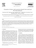
Formation of silicon oxide nanowires directly from au si and pd–au si substrates
Bạn đang xem bản rút gọn của tài liệu. Xem và tải ngay bản đầy đủ của tài liệu tại đây (916.97 KB, 5 trang )
Physica E 37 (2007) 158–162
Formation of silicon oxide nanowires directly from Au/Si and
Pd–Au/Si substrates
Hyun-Kyu Park
a
, Beelyong Yang
a
, Sang-Woo Kim
a,Ã
, Gil-Ho Kim
b
, Doo-Hyeb Youn
c
,
Sang-Hyeob Kim
c
, Sung-Lyul Maeng
c
a
School of Advanced Materials and System Engineering, Kumoh National Institute of Technology, 1 Yangho-dong, Gumi, Gyeongbuk 730-701, South Korea
b
School of Information and Communication Engineering and SKKU Advanced Institute of Nanotechnology, Sungkyunkwan University, Suwon 440-746,
South Korea
c
Cambridge-ETRI Joint R&D Center, Electronics and Telecommunications Research Institute, 161 Gajeong-dong, Daejeon 305-700, South Korea
Available online 9 October 2006
Abstract
Amorphous silicon oxide (SiO
x
) nanowires were directly grown by thermal processing of Si substrates. Au and Pd–Au thin films with
thicknesses of 3 nm deposited on Si (0 0 1) substrates were used as catalysts for the growth of nanowires. High-yield synthesis of SiO
x
nanowires was achieved by a simple heating process (1000–1150 1C) in an Ar ambient atmosphere without introducing any additional Si
source materials. The as-synthesized products were characterized by field-emission scanning electron microscopy, energy-dispersive
X-ray spectroscopy, and transmission electron microscopy measurements. The SiO
x
nanowires with lengths of a few and tens of
micrometers had an amorphous crystal structure. The solid–liquid–solid model of nanowire formation was shown to be valid.
r 2006 Elsevier B.V. All rights reserved.
PACS: 61.46.Àw; 74.62.Bf; 81.07.Àb
Keywords: Silicon oxide; Nanowire; CVD; Silicon substrate
1. Introduction
Studies on the fabrication and characterization of one-
dimensional (1D) nanostructures such as nanowires and
nanotubes have flourished in recent years because of their
fundamental importance to nanotechnology [1,2].A
number of applications using 1D nanostructures have been
investigated for nanoscale devices, devices using flexible
substrates, and sensor applications [3–5] . Recently, silicon
oxide (SiO
x
) nanowires have attracted intens ive interest
due to their novel physical properties and potential
applications in realizing multi-functional nanosized de-
vices, such as blue light emitters and optical sensors with
high sen sitivity [6,7]. Various fabrication methods, includ-
ing laser ablation, chemical vapor deposition, and evapora-
tion, have been used to produce SiO
x
nanowires via a
vapor–liquid–solid (VLS) process requiring Si source
materials [8–10]. In this work, we report simple synthesis
of amorphous SiO
x
nanowires achieved by thermal heating
of Au and Pd–Au coated Si sub strates in an Ar ambient
atmosphere without any additional silicon source supply.
2. Experiments
Si (0 0 1) substrates were used in our experiments. The
substrates were alternately ultrasonically cleaned in acet-
one and in methanol for 5 min, and then dried by nitrogen
blowing. Each 3 nm thin layer of Au and Pd–Au was
deposited on the substrates in a simple sputtering system.
For deposition of the Pd–Au catalyst layer, Pd–Au alloy
(Pd:Au ¼ 1:1) was introduced as the target material. The
substrate was placed in an alumina tube, which was then
heated in a tube furnace at 1000–1150 1C. While heating
the substrates for 90 min, Ar gas with the flow rate of
50 sccm was introduced in the alumina tube at an atmo-
spheric pressure of 760 Torr. After cooling down to room
temperature, a thin layer of white-colored deposit was
ARTICLE IN PRESS
www.elsevier.com/locate/physe
1386-9477/$ - see front matter r 2006 Elsevier B.V. All rights reserved.
doi:10.1016/j.physe.2006.08.003
Ã
Corresponding author. Tel.: +82 54 478 7745; fax: +82 54 478 7769.
E-mail address: (S W. Kim).
found on the substrate surface, indirectly indicating the
formation of SiO
x
nanowires. Measurements utilizing a
field-emission scanning electron microscope (FE-SEM),
equipped with an energy-dispersive X-ray spectroscope
(EDX) as well as a transmission electron microscope
(TEM), were carried out for analysis of the morphology
and atomic composition of the grown nanowires.
3. Results and discussion
Fig. 1 shows FE-SEM images revealing the general
morphologies of the thermally heated Au deposited Si
(0 0 1) [Au/Si] and Pd–Au deposited Si (0 0 1) [Pd–Au/Si]
substrates in the tube furnace. As shown in Fig. 1(a),Au
nanoislands with diameters of 10–80 nm were formed on
the surface of the substrate by heating the Au/Si substrate
at 1000 1C. On the other hand, the formation of Pd–Au
nanoislands with a uniform size distribution (a diameter of
around 100 nm) by heating the Pd–Au/Si substrate at
1000 1C was observed in the FE-SEM measurement
(Fig. 1(b)). From the EDX analysis, it was found that the
formed Pd–Au nanoislands have a dual struc ture consist-
ing of Pd surrounded by Au. In addition, the EDX
spectrum collected from the nanoislands showed the
presence of Au, Pd, Si, and O elements. Interestingly, no
nanowire growth was seen on the Au/Si substrate, while
SiO
x
nanowires were locally formed on the Pd–Au/Si
substrates, as shown in Fig. 1(b), in spite of the same
heating tempe rature of 1000 1C. This fact indicates that the
dual structure consisting of Pd surrounded by Au
facilitates the formation of nanowires.
Fig. 2 shows FE-SEM images revealing the general
morphologies of SiO
x
nanowires grown on Au/Si and
Pd–Au/Si substrates at 1050 1C. As shown in the FE-SEM
images, a large number of nanowires with lengths of tens of
micrometers and diameters around 100 nm were formed
on the Pd–Au/Si substrate surface, while a small number
of nanowires with lengths of a few micrometers were
locally formed on the Au/Si substrate. EDX results in
Fig. 3 show that our SiO
x
nanowires grown on the Au/Si
substrate have an atomic ratio of Si/O higher than the
1
2
of
SiO
2
. On the other hand, the atomic ratio of Si/O in the
SiO
x
nanowires formed on the Pd–Au/Si substrate is nearly
consistent with the
1
2
of SiO
2
, indicating the form ation of
SiO
2
nanowires on the Pd–Au/Si substrate at this growth
temperature.
Since no source of Si vapor existed, and the process
temperature was not high enough to evaporate Si atoms
into the Si substrate, the formation mechanism is different
from the well-known VLS process requiring source
materials and an evaporation technique. In addition, Si
substrates were covered by a thin layer of Pd–Au and Au.
Thus, the possible source for formation of SiO
x
nanowires
comes from the Si substrate, indicating that the formation
mechanism of the SiO
x
nanowires relies on a solid–liquid–
solid (SLS) process. The melting point (MP) of pure Au is
1063 1C. As shown in Fig. 1 , no nanowires were observed
on the Au/Si substrate heated at 1000 1C, while a small
number of nanowires with lengths of a few micrometers
were locally formed on the Au/Si substrate at 1050 1C.
These results suggest that the formation of SiO
x
nanowires
on Si via a SLS process by introducing the Au catalyst is
somewhat limited below the MP of pure Au, even though
the Au–Si eutectic temperature of around 370 1C is much
lower than the process temperature of 1000 1C. On the
other hand, a large number of nanowires were uniformly
formed on the Pd–Au/Si substrate surface in spite of using
a heating temperature lower than the MP of both Au
and Pd (1554 1C). This might be due to enhanced catalytic
activities by Pd–Au alloying compared to pure Au.
ARTICLE IN PRESS
Fig. 1. FE-SEM images revealing general surface morphologies of (a) Au/Si and (b) Pd–Au/Si substrates treated by thermal processing at 1000 1CinanAr
ambient atmosphere in the tube furnace. The scale bar indicates 100 nm.
H K. Park et al. / Physica E 37 (2007) 158–162 159
An efficient diffusion path for Si in the Pd–Au alloy may
result from the formation of many grain crystal boundaries
allowing effective formation of liquid-phased PdSi silicides
(PdSi MP: 972 1C) at the process temperature of 1050 1C
[11–13].
In order to investigate the formation behavior of SiO
x
nanowires on Au/Si and Pd–Au/Si su bstrates at a
temperature above the pure Au MP of 1063 1C, we carried
out thermal heating of Au/Si and Pd–Au/Si substrates at
1100 1C. Fig. 4 shows FE-SEM images of SiO
x
nanowires
grown on Au/Si and Pd–Au/Si substrates, as well as an
EDX spectrum of SiO
x
nanowires grown on the Au/Si
substrate at 1100 1C. At this temperature, twisted SiO
x
nanowires were uniformly formed on both sample surfaces,
although the diameters of SiO
x
nanowires (below 400 nm)
on the Au/Si substrate were larger than those of SiO
x
nanowires (below 200 nm) on the Pd–Au/Si substrate. In
addition, it was found that the SiO
x
nanowires formed on
both substrates at the growth temperature of 1100 1C had a
sharp 1:2 Si to O atomic ratio, which is inconsistent with
the EDX results of the samples grown at 1050 1C. These
facts suggest that Au may play a key role in the formation
of SiO
2
nanowires which form irrespective of introducing
Au or Pd–Au catalyst at a process temperature abo ve the
MP of Au. A more detailed investigation on the catalytic
behavior of Pd for the formation of SiO
x
nanowires will be
reported in the near future.
The formation of the SiO
x
nanowires with such large
diameters might be due to the high process temperature
above the MP of Au. The TEM image (Fig. 5(a)) shows
that the grown SiO
x
nanowires are of an amorphous state.
The highly diffusive ring pattern in the selected-area
electron diffraction (SAED) of the nanowires (Fig. 5(b))
also confirms that they have an amorphous crystal
structure.
ARTICLE IN PRESS
Fig. 2. FE-SEM images revealing general surface morphologies of SiO
x
nanowires grown on (a) Au/Si and (b) Pd–Au/Si substrates at 1050 1CinanAr
ambient atmosphere. The scale bar indicates 1 mm.
Fig. 3. (a) EDX spectrum from the sample presented in Fig. 2(a). The
SiO
x
nanowires on the Au/Si substrate have an atomic ratio of Si/O higher
than the
1
2
of SiO
2
. (b) EDX spectrum from the sample shown in Fig. 2(b).
The atomic ratio of Si/O in the SiO
x
nanowires on the Pd–Au/Si substrate
is nearly consistent with the
1
2
of SiO
2
.
H K. Park et al. / Physica E 37 (2007) 158–162160
The deposited Au thin film can effectively react with the
Si substrate at a temperature above the MP of pure Au,
resulting in the formation of Au–Si eutectic liquid alloy
droplets. Due to the high solubility of Si atoms in the liquid
phase of Au–Si eutectic droplets, a great number of Si
atoms diffuse into the liqui d phase via the interface
between the substrate and the liquid-phased Au–Si
droplets. Compositional supersaturation of the liquid
Au–Si eutectic droplets by the continuous supply of Si
atoms from the substrate results in the formation of SiO
x
nanowires, instead of Si nanowires, due to the lack of
vacuum during the heating process. From the results in this
study, we could conclude that the formation mechanism of
our SiO
x
nanowires is explained by the SLS process.
4. Conclusion
In summary, we have reported amorphous SiO
x
nano-
wires directly grown on Si substrates via the SLS process in
this study. High-yield synthesis of SiO
x
nanowires was
realized by thermal processing of the Au and Pd–Au coated
Si (0 0 1) substrates at 1000–1150 1C in an Ar ambient
atmosphere with no additional Si source materials. The
grown SiO
x
nanowires with diameters ranging from 50 to
400 nm and lengths of a few tens of micrometers had an
amorphous crystal structure. At temperatures below the
MP of pure Au, the catalytic behavior of the Pd–Au
alloying system for growing SiO
x
nanowires was more
active than the Au system. On the other hand, Au played
ARTICLE IN PRESS
Fig. 4. FE-SEM images of nanowires on (a) Au/Si and on (b) Pd–Au/Si, and (c) an EDX spectrum of the SiO
x
nanowires (sample shown in (a)) grown at
1100 1C in an Ar ambient atmosphere. The scale bar indicates 1 mm.
H K. Park et al. / Physica E 37 (2007) 158–162 161
an important role in the formation of SiO
x
nanowires at
process temperatures above the MP of Au, indicating the
comparatively weakened catalytic behavior of Pd.
Acknowledgments
This work was supported by the Ministry of Information
and Communication, Republic of Korea, under Project no.
A1100-0501-0073. The authors thank Dr. J. M. Yang for
TEM characterization.
References
[1] S. Iijima, Nature 354 (1991) 56.
[2] M.H. Huang, S. Mao, H. Feick, H. Yan, Y. Wu, H. Kind, E. Weber,
R. Russo, P. Yang, Science 292 (2001) 1897.
[3] Y. Cui, Z. Zhong, D. Wang, W.U. Wang, C.M. Lieber, Nano Lett. 3
(2003) 149.
[4] X. Duan, C. Niu, V. Sahl, J. Chen, J.W. Parce, S. Empedocles,
J.L. Goldman, Nature 425 (2003) 274.
[5] Y.X. Liang, Y.J. Chen, T.H. Wang, Appl. Phys. Lett. 85 (2004) 666.
[6] D.P. Yu, Q.L. Hang, H.Z. Zhang, Z.G. Bai, J.J. Wang, Y.H. Zou,
W. Qian, G.C. Xiong, S.Q. Feng, Appl. Phys. Lett. 73 (1998)
3076.
[7] L. Tong, J. Lou, R.R. Gattas, S. He, X. Chen, L. Liu, E. Mazur,
Nano Lett. 5 (2005) 259.
[8] A.M. Morales, C.M. Lieber, Science 279 (1998) 208.
[9] Z.Q. Liu, S.S. Xie, L.F. Sun, D.S. Tang, W.Y. Zhou, C.Y. Wang,
W. Liu, Y.B. Li, X.P. Zou, G. Wang, J. Mater. Res. 16 (2001)
683.
[10] N. Wang, Y.H. Tang, Y.F. Zhang, C.S. Lee, S.T. Lee, Phys. Rev. B
58 (1998) R16024.
[11] Z.Q. Liu, Z.W. Pan, L.F. Sun, D.S. Tang, W.Y. Zhou, G. Wang,
L.X. Qian, S.S. Xie, J. Phys. Chem. Solids 61 (2000) 1171.
[12] J.L. Elechiguerra, J.A. Manriquez, M.J. Yacaman, Appl. Phys. A:
Mater. Sci. Process. 79 (2004) 461.
[13] D.K. Sood, P.K. Sekhar, S. Bhansali, Appl. Phys. Lett. 88 (2006)
143110.
ARTICLE IN PRESS
Fig. 5. (a) TEM image of a single amorphous SiO
x
nanowire grown on the Pd–Au/Si substrate (Fig. 4(b)). (b) SAED pattern revealing the amorphous
nature of the SiO
x
nanowires.
H K. Park et al. / Physica E 37 (2007) 158–162162