- Trang chủ >>
- Khoa Học Tự Nhiên >>
- Vật lý
recent advances in wide bandgap semiconductor biological and gas sensors
Bạn đang xem bản rút gọn của tài liệu. Xem và tải ngay bản đầy đủ của tài liệu tại đây (3.58 MB, 59 trang )
Recent advances in wide bandgap semiconductor
biological and gas sensors
S.J. Pearton
a,
*
, F. Ren
b
, Yu-Lin Wang
b
, B.H. Chu
b
, K.H. Chen
b
, C.Y. Chang
b
,
Wantae Lim
a
, Jenshan Lin
c
, D.P. Norton
a
a
Department of Materials Science and Engineering, University of Florida, Gainesville, FL 32611, USA
b
Department of Chemical Engineering, University of Florida, Gainesville, FL 32611, USA
c
Department of Electrical and Computer Engineering, University of Florida, Gainesville, FL 32611, USA
article info
Article history:
Received 10 June 2009
Received in revised form 27 August 2009
Accepted 28 August 2009
abstract
There has been significant recent interest in the use of surface-
functionalized thin film and nanowire wide bandgap semiconduc-
tors, principally GaN, InN, ZnO and SiC, for sensing of gases, heavy
metals, UV photons and biological molecules. For the detection of
gases such as hydrogen, the semiconductors are typically coated
with a catalyst metal such as Pd or Pt to increase the detection sen-
sitivity at room temperature. Functionalizing the surface with oxi-
des, polymers and nitrides is also useful in enhancing the detection
sensitivity for gases and ionic solutions. The wide energy bandgap
of these materials make them ideal for solar-blind UV detection,
which can be of use for detecting fluorescence from biotoxins.
The use of enzymes or adsorbed antibody layers on the semicon-
ductor surface leads to highly specific detection of a broad range
of antigens of interest in the medical and homeland security fields.
We give examples of recent work showing sensitive detection of
glucose, lactic acid, prostate cancer and breast cancer markers
and the integration of the sensors with wireless data transmission
systems to achieve robust, portable sensors.
Ó 2009 Elsevier Ltd. All rights reserved.
Contents
1. Introduction . . . 2
2. Gas sensing. . . . 4
0079-6425/$ - see front matter Ó 2009 Elsevier Ltd. All rights reserved.
doi:10.1016/j.pmatsci.2009.08.003
* Corresponding author.
E-mail address: fl.edu (S.J. Pearton).
Progress in Materials Science 55 (2010) 1–59
Contents lists available at ScienceDirect
Progress in Materials Science
journal homepage: www.elsevier.com/locate/pmatsci
2.1. H
2.
sensing . 4
2.2. O
2
sensing . 12
2.3. CO
2
sensing 13
2.4. CH
4
sensing 15
3. UV photodetectors . . . . . . . . . 17
3.1. UV photoresponse of single ZnO nanowires . . . . . . . . . . . . 18
4. Sensor functionalization . . . . 20
5. pH measurement . . . . . . . . . . 23
6. Exhaled breath condensate . . 27
7. Heavy metal detection . . . . . . 27
8. Biotoxin sensors . . . . . . . . . . . 32
8.1. Botulinum . 33
9. Biomedical applications . . . . . 34
9.1. Prostate cancer detection . . . . . . . . 40
9.2. Kidney injury molecule detection . 41
9.2.1. Breast cancer. . . . . . 43
9.2.2. Lactic acid . . . . . . . . 45
9.2.3. Chloride ion detection . . . . . . . . . . . . . . . . . 47
9.2.4. Pressure sensing . . . 49
9.3. Traumatic brain injury . . . . . . . . . . 50
10. Wireless sensors. . . . . . . . . . 51
11. Summary and conclusions. . 54
Acknowledgments . . . . . . . . . 55
References . . . . . . . . . . . . . . . 55
1. Introduction
Chemical sensors have gained in importance in the past decade for applications that include home-
land security, medical and environmental monitoring and also food safety. A desirable goal is the abil-
ity to simultaneously analyze a wide variety of environmental and biological gases and liquids in the
field and to be able to selectively detect a target analyte with high specificity and sensitivity. In the
area of detection of medical biomarkers, many different methods, including enzyme-linked immun-
sorbent assay (ELISA), particle-based flow cytometric assays, electrochemical measurements based
on impedance and capacitance, electrical measurement of micro-cantilever resonant frequency
change, and conductance measurement of semiconductor nanostructures. gas chromatography (GC),
ion chromatography, high density peptide arrays, laser scanning quantitative analysis, chemilumines-
cence, selected ion flow tube (SIFT), nanomechanical cantilevers, bead-based suspension microarrays,
magnetic biosensors and mass spectrometry (MS) have been employed [1–9]. Depending on the sam-
ple condition, these methods may show variable results in terms of sensitivity for some applications
and may not meet the requirements for a hand-held biosensor.
For homeland security applications, reliable detection of biological agents in the field and in real
time is challenging. During the anthrax attack on the World Bank in 2002, field tests showed 1200
workers to be positive, and all were sent home. One hundred workers were provided antibiotics. How-
ever, confirmatory testing showed zero positives. False positives and false negatives can result due to
very low volumes of samples available for testing and poor device sensitivities. Toxins such as ricin,
botulinum toxin or enterotoxin B are environmentally stable, can be mass-produced and do not need
advanced technologies for production and dispersal. The threat of these toxins is real. This is evident
from the recent ricin detection from White House mail facilities and a US senator’s office. Terrorists
have already attempted to use botulinum toxin as a bio-weapon. Aerosols were dispersed at multiple
sites in Tokyo, and at US military installations in Japan on at least 3 occasions between 1990 and 1995
by the Japanese cult Aum Shinrikyo [10]. Four of the countries listed by the US government as ‘‘state
sponsors of terrorism” (Iran, Iraq, North Korea, and Syria) [10] have developed, or are believed to be
developing, botulinum toxin as a weapon [11,12]. After the 1991 Persian Gulf War, Iraq admitted to
2 S.J. Pearton et al. / Progress in Materials Science 55 (2010) 1–59
the United Nations inspection team to having produced 19,000 L of concentrated botulinum toxin, of
which approximately 10,000 L were loaded into military weapons. This toxin has not been fully ac-
counted for and constitutes approximately three times the amount needed to kill the entire current
human population by inhalation [10]. A significant issue is the absence of a definite diagnostic method
and the difficulty in differential diagnosis from other pathogens that would slow the response in case
of a terror attack. This is a critical need that has to be met to have an effective response to terrorist
attacks. Given the adverse consequences of a lack of reliable biological agent sensing on national secu-
rity, there is a critical need to develop novel, more sensitive and reliable technologies for biological
detection in the field [13,14]. Some specific toxins of interest include Enterotoxin type B (Category
B, NIAID), Botulinum toxin (Category A NIAID) and ricin (Category B NIAID).
While the techniques mentioned above show excellent performance under lab conditions, there is
also a need for small, hand-held sensors with wireless connectivity that have the capability for fast
responses. The chemical sensor market represents the largest segment for sales of sensors, including
chemical detection in gases and liquids, flue gas and fire detection, liquid quality sensors, biosensors
and medical sensors. Some of the major applications in the home include indoor air quality and nat-
ural gas detection. Attention is now being paid to more demanding applications where a high degree
of chemical specificity and selectivity is required. For biological and medical sensing applications, dis-
ease diagnosis by detecting specific biomarkers (functional or structural abnormal enzymes, low
molecular weight proteins, or antigen) in blood, urine, saliva, or tissue samples has been established.
Most of the techniques mentioned earlier such as ELISA possesses a major limitation in that only one
analyte is measured at a time. Particle-based assays allow for multiple detection by using multiple
beads but the whole detection process is generally longer than 2 h, which is not practical for in-office
or bedside detection. Electrochemical devices have attracted attention due to their low cost and sim-
plicity, but significant improvements in their sensitivities are still needed for use with clinical sam-
ples. Micro-cantilevers are capable of detecting concentrations as low as 10 pg/ml, but suffer from
an undesirable resonant frequency change due to the viscosity of the medium and cantilever damping
in the solution environment. Nano-material devices have provided an excellent option toward fast, la-
bel-free, sensitive, selective, and multiple detections for both preclinical and clinical applications.
Examples of detection of biomarkers using electrical measurements with semiconductor devices in-
clude carbon nanotubes for lupus erythematosus antigen detection [4], compound semiconducting
nanowires and In
2
O
3
nanowires for prostate-specific antigen detection [5], and silicon nanowire arrays
for detecting prostate-specific antigen [9]. In clinical settings, biomarkers for a particular disease state
can be used to determine the presence of disease as well as its progress.
Semiconductor-based sensors can be fabricated using mature techniques from the Si chip industry
and/or novel nanotechnology approaches. Silicon based sensors are still the dominant component of
the semiconductor segment due to their low cost, reproducible and controllable electronic response.
However, these sensors are not suited for operation in harsh environments, for instance, high temper-
ature, high pressure or corrosive ambients. Si will be etched by some of the acidic or basic aqueous
solutions encountered in biological sensing. By sharp contrast, GaN is not etched by any acid or base
at temperatures below a few hundred degrees. Therefore, wide band-gap group III nitride compound
semiconductors (AlGaInN materials system) are alternative options to supplement silicon in these
applications because of their chemical resistance, high temperature/high power capability, high elec-
tron saturation velocity and simple integration with existing GaN-based UV light-emitting diode, UV
detectors and wireless communication chips.
A promising sensing technology utilizes AlGaN/GaN high electron mobility transistors (HEMTs).
HEMT structures have been developed for use in microwave power amplifiers due to their high
two-dimensional electron gas (2DEG) mobility and saturation velocity. The conducting 2DEG channel
of AlGaN/GaN HEMTs is very close to the surface and extremely sensitive to adsorption of analytes.
HEMT sensors can be used for detecting gases, ions, pH values, proteins, and DNA.
The GaN materials system is attracting much interest for commercial applications of green, blue, and
UV light-emitting diodes (LEDs), laser diodes as well as high speed and high frequency power devices.
Due to the wide-bandgap nature of the material, it is very thermally stable, and electronic devices can
be operated at temperatures up to 500 °C. The GaN-based materials are also chemically stable, and no
known wet chemical etchant can etch these materials; this makes them very suitable for operation in
S.J. Pearton et al. / Progress in Materials Science 55 (2010) 1–59
3
chemically harsh environments. Due to the high electron mobility, GaN material based high electron
mobility transistors (HEMTs) can operate at very high frequency with higher breakdown voltage, better
thermal conductivity, and wider transmission bandwidths than Si or GaAs devices [15–17].
An overlooked potential application of the GaN HEMT structure is sensors. The high electron sheet
carrier concentration of nitride HEMTs is induced by piezoelectric polarization of the strained AlGaN
layer in the hetero-junction structure of the AlGaN/GaN HEMT and the spontaneous polarization is
very large in wurtzite III-nitrides. This provides an increased sensitivity relative to simple Schottky
diodes fabricated on GaN layers or field effect transistors (FETs) fabricated on the AlGaN/GaN HEMT
structure. The gate region of the HEMT can be used to modulate the drain current in the FET mode
or use as the electrode for the Schottky diode. A variety of gas, chemical and health-related sensors
based on HEMT technology have been demonstrated with proper surface functionalization on the gate
area of the HEMTs, including the detection of hydrogen, mercury ion, prostate-specific antigen (PSA),
DNA, and glucose [18–58].
In this review, we discuss recent progress in the functionalization of these semiconductor sensors
for applications in detection of gases, pH measurement, biotoxins and other biologically important
chemicals and the integration of these sensors into wireless packages for remote sensing capability.
2. Gas sensing
2.1. H
2.
sensing
There is great interest in detection of hydrogen sensors for use in hydrogen-fueled automobiles and
with proton-exchange membrane (PEM) and solid oxide fuel cells for space craft and other long-term
sensing applications. These sensors are required to detect hydrogen near room temperature with min-
imal power consumption and weight and with a low rate of false alarms. Due to their low intrinsic
carrier concentrations, GaN- and SiC-based wide band gap semiconductor sensors can be operated
at lower current levels than conventional Si-based devices and offer the capability of detection to
$600 °C [18–36].
Unlike conventional sensors where the changes of the sensing material’s conductivity or resistivity
are used to detect the gas concentration, by integrating the gas sensing material such as Pd or Pt metal
on the gate electrode of the HEMTs, the change of the sensing material’s conductivity can be amplified
through Schottky diode or FET operation. It is generally accepted that H
2
is dissociated when adsorbed
on Pt and Pd at room temperature. The reaction is as follows:
H
2ðadsÞ
! 2H
þ
þ e
À
Dissociated hydrogen causes a change in the channel and conductance change. This makes the inte-
grated semiconductor device based sensors extremely sensitive and the sensors have a broad dynamic
range of the sensing concentration. A surface covered reference semiconductor device can also be eas-
ily fabricated side-by-side with sensing device to eliminate the temperature variation of the ambient
and the fluctuation of the supplied voltage to the sensors [20].
Fig. 1 shows a schematic of a Schottky diode hydrogen sensor on AlGaN/GaN HEMT layer structure
and a photograph of packaged sensors. The layer structure included an initial 2
l
m thick undoped GaN
buffer followed by a 35 nm thick unintentionally doped Al
0.28
Ga
0.72
N layer. Mesa isolation was
achieved by using an inductively coupled plasma system with Ar/Cl
2
based discharges. The Ohmic
contacts were formed by lift-off of sputtered Ti/Al/TiB
2
/Ti/Au, followed by annealing at 850 °C for
45 s under a flowing N
2
ambient [21]. A thin (100 Å) Pt Schottky contact was deposited by e-beam
evaporation for the Schottky metal. The final step was deposition of e-beam evaporated Ti/Au inter-
connection contacts. The individual devices were diced and wire-bonded to carriers.
The sensor carrier was then placed in our test chamber. Mass flow controllers were used to control
the gas flow through the chamber, and the devices were exposed to either 100% pure N
2
,or1%H
2
in nitrogen. Fig. 2 shows the linear (top) and log scale (bottom) forward current–voltage (I–V)
characteristics at 25 °C of the HEMT diode, both in air and in a 1%H
2
in air atmosphere. For these
diodes, the current increases upon introduction of the H
2
, through a lowering of the effective barrier
height. The data was fit to the relations for thermionic emission and showed decreases in Schottky
4 S.J. Pearton et al. / Progress in Materials Science 55 (2010) 1–59
barrier height
U
B
of 30–50 meV at 50 °C and larger changes at higher temperatures. The decrease in
barrier height is completely reversible upon removing the H
2
from the ambient and results from dif-
fusion of atomic hydrogen to the metal/GaN interface, altering the interfacial charge.
The H
2
catalytically decomposes on the Pt metallization and diffuses rapidly to the interface where
it forms a dipole layer. The changes in forward diode current upon introduction of the hydrogen into
the ambient is $1 mA over the diode bias voltage above 1 V, as shown in Fig. 2 (left). As illustrated in
Fig. 2. Time response of differential GaN sensor to introduction of 1% H
2
in air ambient.
Fig. 1. Cross-sectional schematic of completed Schottky diode on AlGaN/GaN HEMT layer structure (top) and plan-view
photograph of device (bottom).
S.J. Pearton et al. / Progress in Materials Science 55 (2010) 1–59
5
the Fig. 2 (right), the change of the diode current was significantly lower when the bias voltage was
below 1 V. This low current operation offers the ability of lower power hydrogen detection.
Fig. 3 shows time response of diode forward current at a fixed bias of 0.6 V when switching back
and forth between the ambient from N
2
to 1%H
2
balanced with nitrogen. The change in forward cur-
rent for the diode was in the micro-amp range with a bias voltage of 0.6 V, which was corresponding
to a power consumption of 3.6
l
W. The response time was less than 1 s. It took sometime to purge out
the hydrogen from the gas chamber, therefore the recovery time was longer than the response time.
Using the same layer structure, the sensor can also be fabricated as a field effect transistor. Excel-
lent response time and repeatability were also achieved, as illustrated in Fig. 3 (bottom).
To achieve the goal of detecting reactions due to hydrogen only and excluding other changes
caused by variables such as temperature and moisture, a differential detection interface was used.
Several kinds of differential devices have been fabricated and each of its performance has been eval-
uated to select the most effective solution. These differential devices have two sensors integrated on
the same chip. The two sensors are identical except one is designed to react to hydrogen whereas the
0 50 100 150 200
6.7
6.8
6.9
7.0
7.1
7.2
other one is covered by dielectric protection layer and not exposed to ambient gas. Fig. 1(bottom)
shows the die photo of a differential sensor device with a reference diode. One sensor reacted
promptly with the exposure of hydrogen while the other, the reference diode, had no significant re-
sponse as expected, proving the functionality of the differential sensor.
W/Pt contacted GaN Schottky diodes also show forward current changes of >1 mA at low bias (3 V)
in the temperature range 350–600 °C when the measurement ambient is changed from pure N
2
to
10%H
2
/90%N
2
. We have found that use of a metal–oxide-semiconductor(MOS) diode structure with
Sc
2
O
3
gate dielectric and the same W/Pt metallization show these same reversible changes in forward
current upon exposure to H
2
-containing ambients over a much broader temperature range (90 to
>625 °C). The increase in current in both cases is the result of a decrease in effective barrier height
of the MOS and Schottky gates of 30–50 mV 10%H
2
/90%N
2
ambients relative to pure N
2
and is due
to catalytic dissociation of the H
2
on the Pt contact, followed by diffusion to the W/GaN or Sc
2
O
3
/
GaN interface. The presence of the oxide lowers the temperature at which the hydrogen can be de-
tected and in conjunction with the use of the high temperature stable W metallization enhances
0.0 0.2 0.4 0.6 0.8 1.0 1.2 1.4
0
2
4
6
8
10
12
Current(mA)
Bias Voltage(V)
Nitrogen
10% Hydrogen
T = 500
o
C
0.0 0.2 0.4 0.6 0.8 1.0 1.2 1.4
0
2
4
6
8
10
12
Current(mA)
Bias Voltage(V)
Nitrogen
10% Hydrogen
T = 500
o
C
Fig. 4. Change in current in W/Pt GaN and AlGaN/GaN diodes at 500 °C when the ambient is switched from N
2
to 10% H
2
in N
2
.
S.J. Pearton et al. / Progress in Materials Science 55 (2010) 1–59
7
the potential applications of these wide bandgap sensors. Fig. 4 shows that the relative change in cur-
rent is larger with the MOS structure. SiC Schottky diodes with Pd or Pt contacts are also sensitive to
the presence of hydrogen in the ambient, as shown in Fig. 5. The advantage of the nitride system rel-
ative to SiC is the availability of a heterostructure and the strong piezoelectric and polarization fields
present in the nitrides that enhance their capability for chemical sensing.
We have also found that nanostructured wide bandgap materials functionalized with Pd or Pt are
even sensitive than their thin film counterparts because of the large surface-to-volume ratio [30,31].
1-D semiconductor nanomaterials, such as carbon nanotubes (CNTs), Si nanowires, GaN nanowires,
and ZnO nanowires are good candidates to replace 2-D semiconductors due to several advantages. First,
1-D structure has large surface-to-volume ratio which means that a significant fraction of the atoms can
participate in surface reactions. Second, the Debye length (k
D
) for 1-D nanomaterial is comparable to
their radius over a wide temperature and doping range, which causes them moresensitivethan 2-D thin
film. Third, 1-D nanostructure is usually stoichiometrically controlled better than 2-D thin film, and has
a greater level of crystallinity than the 2-D thin-film. With 1-D structures, common defect problems in
Fig. 5. Pt/SiC Schottky diode (top) and change in current at fixed bias of 1.5 V when the ambient is switched from air to 10% H
2
in air.
8 S.J. Pearton et al. / Progress in Materials Science 55 (2010) 1–59
2-D semiconductors could be easily solved. Fourth, further decreasing the diameter, onset of quantum
effects is expected to be appeared. Finally, low cost and lowpowerconsumption,and highcompatibility
with microelectronic processing make 1-D nanostructure potential and practical materials of sensors.
Impressive results have been demonstrated with GaN, InN and ZnO nanowires or nanobelts that are
sensitive to hydrogen down to approximately 20 ppm at room temperature. As an example, Fig. 6 (top)
shows scanning electron microscopy (SEM) micrographs of as-grown nanowires. A layer of 10 nm-
thick Pd was deposited by sputtering onto the nanowires to verify the effect of catalyst on gas sensi-
tivity. The bottom of Fig. 6 shows the measured resistance at a bias of 0.5 V as a function of time from
Pd-coated and uncoated multiple GaN nanowires exposed to a series of H
2
concentrations (200–
1500 ppm) in N
2
for 10 min at room temperature. Pd-coating of the nanowires improved the sensitiv-
ity to ppm level H
2
by a factor of up to 11. The addition of Pd appears to be effective in catalytic dis-
sociation of molecular hydrogen. Diffusion of atomic hydrogen to the metal/GaN interface alters the
surface depletion of the wires and hence the resistance at fixed bias voltage [59]. The resistance
change depended on the gas concentration but the variations were small at H
2
concentration above
Fig. 6. SEM images of as-grown GaN nanowires (top) and measured resistance at an applied bias of 0.5 V as a function of time
from Pd-coated and uncoated multiple GaN nanowires exposed to a series of H
2
concentrations (200–1500 ppm) in N
2
for
10 min at room temperature.
S.J. Pearton et al. / Progress in Materials Science 55 (2010) 1–59
9
1000 ppm. The resistance after exposing the nanowires to air was restored to approximately 90% of
initial level within 2 min [30,31].
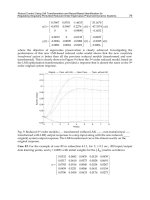
Similar results can be obtained with InN nanostructures. The hydrogen sensing characteristics of
multiple InN nanobelts grown by Metalorganic Chemical Vapor Deposition have been reported previ-
ously [29,60]. Pt-coated InN sensors could selectively detect hydrogen at the tens of ppm level at 25 °C
while uncoated InN showed no detectable change in current when exposed to hydrogen under the
same conditions. Upon exposure to various concentrations of hydrogen (20–300 ppm) in N
2
ambient,
the relative resistance change increased from 1.2% at 20 ppm H
2
to 4% at 300 ppm H
2
, as shown in
Fig. 7. (Top) X-ray diffraction spectrum of MOCVD-grown InN nanobelts (the inset shows SEM images of the nanobelts) and
change in current at fixed bias for switching from 20 to 300 ppm H
2
in air to pure air (bottom).
10 S.J. Pearton et al. / Progress in Materials Science 55 (2010) 1–59
Fig. 7. Approximately 90% of the initial InN resistance was recovered within 2 min by exposing the
nanobelts to air. Temperature-dependent measurements showed larger resistance change and faster
response at high temperature compared to those at room temperature due to increase in catalytic dis-
sociation rate of H
2
as well as diffusion rate of atomic hydrogen into the Pt/InN interface. The Pt-
coated InN nanobelt sensors were operated at low power levels ($0.5 mW).
Fig. 8 shows a schematic of single ZnO nanowire sensor, an SEM micrograph and the time dependence
of resistance of Pt-coated ZnO nanowires as the gas ambient is switched from N
2
to various concentra-
tions of H
2
in N
2
(10–500 ppm) as time proceeds. There are several aspects that are noteworthy. First,
there is a strong increase (approximately a factor of 10) in the response of the Pt-coated nanowires to
hydrogen relative to the uncoated devices. The addition of the Pt appears to be effective in catalytic
0306090120150
-0.04
-0.03
-0.02
-0.01
0.00
0.01
H
2
H
2
H
2
H
2
ZnO nanorod with Pd
Air
Air
Air
Air
O
2
500ppm
250ppm
100ppm
10ppm
N
2
Delta R/R (Sensitivity)
Time(min)
Fig. 8. Schematic of ZnO nanowire sensor (top), SEM of completed device (center) and change in resistance as a function of time
when switching to H
2
-containing ambients.
S.J. Pearton et al. / Progress in Materials Science 55 (2010) 1–59
11
dissociation of the H
2
to atomic hydrogen. Second, there was no response of either type of nanowires to
the presence of O
2
in the ambient at room temperature. Third, the effective conductivity of the Pt-coated
nanowires is higher due to the presence of the metal. Fourth, the recovery of the initial resistance is rapid
(90%, <20 s) upon removal of the hydrogen from the ambientby either O
2
or air, while the nanowire resis-
tance is still changing at least 15 min after the introduction of the hydrogen. The reversible chemisorp-
tion of reactive gases at the surface of metal oxides such as ZnO can produce a large and reversible
variation in the conductance of the material. The gas sensing mechanism suggested include the desorp-
tion of adsorbed surface hydrogen and grain boundaries in poly-ZnO, exchange of charges between ad-
sorbed gas species and the ZnO surface leading to changes in depletion depth and changes in surface or
grain boundary conduction by gas adsorption/desorption [60–64]. The detection mechanism is still not
firmly established in these devices and needs further study. It should be remembered that hydrogen
introduces a shallow donor state in ZnO and this change innear-surface conductivitymay also play a role.
2.2. O
2
sensing
The current technology for O
2
measurement, referred to as oximetry, is small and convenient to
use. However, the O
2
measurement technology does not provide a complete measure of respiratory
sufficiency. A patient suffering from hypoventilation (poor gas exchange in the lungs) given 100% oxy-
gen can have excellent blood oxygen levels while still suffering from respiratory acidosis due to exces-
sive CO
2
. The O
2
measurement is also not a complete measure of circulatory sufficiency. If there is
insufficient blood flow or insufficient hemoglobin in the blood (anemia), tissues can suffer hypoxia de-
spite high oxygen saturation in the blood that does arrive. The current oxide-based O
2
sensors can
operate at very high temperatures, such as the commercialized solid electrolyte ZrO
2
(700 °C) or the
semiconductor metal oxides such as TiO
2
,Nb
2
O
5
, SrTiO
3
, and CeO
2
(>400 °C). However, it remains
important to develop a low operation temperature and high sensitivity O
2
sensor to build a small, por-
table and low cost O
2
sensor system for biomedical applications.
Oxide-based materials are widely used and studied for oxygen sensing because of their low cost
and good reliability. The commercialized solid electrolyte ZrO
2
[65] has been widely used in automo-
biles for oxygen sensing in combustion processes. The electrolyte metal oxide oxygen sensor usually
uses a reference gas and operates at high temperature (700 °C) [66]. Semiconductor metal oxides such
as TiO
2
,Ga
2
O
3
,Nb
2
O
5
, SrTiO
3
, and CeO
2
do not need the reference gas, but they still need to be oper-
ated at a considerably high temperature (>400 °C) in order to reach high sensitivity, which means a
high power consumption for heating up the sensors [67–72]. For biomedical applications, such as
monitoring oxygen in the breath for a lung transplant patient, a portable and low power consumption
O
2
sensor system is needed. Therefore, it is crucial to develop a low operating temperature and high
sensitivity O
2
sensor for those applications.
The conductivity mechanism of most metal oxides based semiconductors results from electron
hopping from intrinsic defects in the oxide film and these defects are related to the oxygen vacancies
generated during oxide growth. Typically, the higher the concentration of oxygen vacancies in the
oxide film, the more conductive is the film. InZnO (IZO) films have been used in fabricating thin film
transistors and the conductivity of the IZO is also found to depend on the oxygen partial pressure dur-
ing the oxide growth [73–75]. The IZO is a good candidate for O
2
sensing applications.
The schematic of the oxygen sensor is shown at the top of Fig. 9. The bottom part of the figure
shows the device had a strong response when it was tested at 120 °C in pure nitrogen and pure oxygen
alternately at Vds = 3 V. When the device was exposed to the oxygen, the drain-source current de-
creased, whereas when the device was exposed to nitrogen, the current increased. The IZO film pro-
vides a high oxygen vacancy concentration, which makes the film readily sense oxygen and create a
potential on the gate area of the AlGaN/GaN HEMT. A sharp drain-source current change demonstrates
the combination of the advantage of the high electron mobility of the HEMT and the high oxygen va-
cancy concentration of the IZO film. Because of these advantages, this oxygen sensor can operate with
a high sensitivity at a relatively low temperature compared to many oxide-based oxygen sensors
which operate from 400 °C to 700 °C.
In summary, it is clear that through a combination of IZO films and the AlGaN/GaN HEMT structure,
a low operation temperature and low power consumption oxygen sensor can be achieved. The sensor
12 S.J. Pearton et al. / Progress in Materials Science 55 (2010) 1–59
can be either used in the steady-state or in the annealed mode which provide flexibility in various
applications. This device shows promise for portable, fast response and high sensitivity oxygen
detectors.
2.3. CO
2
sensing
The detection of carbon dioxide (CO
2
) gas has attracted attention in the context of global warming,
biological and health-related applications such as indoor air quality control, process control in fermen-
tation, and in the measurement of CO
2
concentrations in patients’ exhaled breath with lung and stom-
ach diseases [76–79]. In medical applications, it can be critical to monitor the CO
2
and O
2
concentrations in the circulatory systems for patients with lung diseases in the hospital. The current
technology for CO
2
measurement typically uses IR instruments, which can be very expensive and
bulky.
The most common approach for CO
2
detection is based on non-dispersive infrared (NDIR) sensors,
which are the simplest of the spectroscopic sensors [80–83]. The best detection limits for the NDIR
sensors are currently in the range of 20–10,000 ppm. The key components of the NDIR approach
are an infrared (IR) source, a light tube, an interference filter, and an infrared (IR) detector. In opera-
tion, gas enters the light tube. Radiation from the IR light source passes through the gas in the light
tube to impinge on the IR detector. The interference filter is positioned in the optical path in front
of the IR detector such that the IR detector receives the radiation of a wavelength that is strongly ab-
sorbed by the gas whose concentration is to be determined while filtering out the unwanted wave-
lengths. The IR detector produces an electrical signal that represents the intensity of the radiation
Fig. 9. Schematic of AlGaN/GaN HEMT based O
2
sensor (top) and drain current of IZO functionalized HEMT sensor measured at
fixed source-drain during the exposure to different O
2
concentration ambients. The drain bias voltage was 0.5 V and
measurements were conducted at 117 °C.
S.J. Pearton et al. / Progress in Materials Science 55 (2010) 1–59
13
impinging upon it. It is generally considered that the NDIR technology is limited by power consump-
tion and size.
In recent years, monomers or polymers containing amino-groups, such as tetrakis(hydroxy-
ethyl)ethylenediamine, tetraethylene-pentamine and polyethyleneimine (PEI) have been used for
CO
2
sensors to overcome the power consumption and size issues found in the NDIR approach [84–
88]. Most of the monomers or polymers are utilized as coatings of surface acoustic wave transducers.
The polymers are capable of adsorbing CO
2
and facilitating a carbamate reaction. PEI has also been
used as a coating on carbon nanotubes for CO
2
sensing by measuring the conductivity of nanotubes
upon exposing to the CO
2
gas. For example, CO
2
adsorbed by a PEI coated nanotube portion of a NTFET
(nanotube field effect transistor) sensor lowers the total pH of the polymer layer and alters the charge
transfer to the semiconducting nanotube channel, resulting in the change of NTFET electronic charac-
teristics [89–92].
A schematic cross-section of the device is shown in Fig. 10. The interaction between CO
2
and amino
group-containing compounds with the influence of water molecules is based on an acid–base reaction.
The purpose of adding starch into the PEI in our experiment was to enhance the absorption of the
water molecules into the PEI/starch thin film. Several possible reaction mechanisms have been sug-
gested. The key reaction was that primary amine groups, –NH
2
, on the PEI main chain reacted with
CO
2
and water forming –NH
3
+
ions and the CO
2
molecule became OCOOH
À
ions. Thus, the charges,
Fig. 10. Schematic of AlGaN/GaN HEMT based CO
2
sensor (top) and drain current of PEI/starch functionalized HEMT sensor
measured at fixed source-drain during the exposure to different CO
2
concentration ambients. The drain bias voltage was 0.5 V
and measurements were conducted at 108 °C.
14 S.J. Pearton et al. / Progress in Materials Science 55 (2010) 1–59
or the polarity, on the PEI main chain were changed. The electrons in the two-dimensional electron gas
(2DEG) channel of the AlGaN/GaN HEMT are induced by piezoelectric and spontaneous polarization
effects. This 2DEG is located at the interface between the GaN layer and AlGaN layer. There are positive
counter charges at the AlGaN surface layer induced by the 2DEG. Any slight changes in the ambient of
the AlGaN/GaN HEMT affect the surface charges of the AlGaN/GaN HEMT. The PEI/starch was coated
on the gate region of the HEMT. The charges of the PEI changed through the reactions between –NH
2
and CO
2
as well as water molecules. These are then transduced into a change in the concentration of
the 2DEG in the AlGaN/GaN HEMTs.
Fig. 10 (bottom) shows the drain current of PEI/starch functionalized HEMT sensors measured ex-
posed to different CO
2
concentration ambients. The measurements were conducted at 108 °C and a
fixed source-drain bias voltage of 0.5 V. The current increased with the introduction of CO
2
gas. This
was due to the net positive charges increased on the gate area, thus inducing electrons in the 2DEG
channel. The response to CO
2
gas has a wide dynamic range from 0.9% to 50%. Higher CO
2
concentra-
tions were not tested because there is little interest in these for medical related applications. The re-
sponse times were on the order of 100 s. The signal decay time was slower than the rise time and was
due to the longer time required to purge CO
2
out from the test chamber.
The effect of ambient temperature on CO
2
detection sensitivity was investigated. The drain current
changes were linearly proportional to the CO
2
concentration for all the tested temperatures. However,
the HEMT sensors showed higher sensitivity for the higher testing temperatures. There was a notice-
able change of the sensitivity from the sensors tested at 61 °C to those tested at 108 °C. This difference
is likely due to higher ambient temperature increasing the reaction rate between amine groups and
CO
2
as well as the diffusion of CO
2
molecules into the PEI thin film. The sensors exhibited reversible
and reproducible characteristics.
In conclusion, PEI/starch functionalized HEMT sensors for CO
2
detection with a wide dynamic range
from 0.9% to 50%. The sensors were operated at low bias voltage (0.5 V) for low power consumption
applications. The sensors showed higher sensitivity at the testing temperature higher than $100 °C.
The sensors showed good repeatability. This electronic detection of CO
2
gas is a significant step to-
wards a compact sensor chip, which can be integrated with a commercial available hand-held wireless
transmitter to realize a portable, fast and high sensitive CO
2
sensor.
2.4. CH
4
sensing
Of particular interest in developing wide bandgap sensors are methods for detecting ethylene
(C
2
H
4
), which offers problems because of its strong double bonds and hence the difficulty in dissoci-
ating it at modest temperatures [93–95]. Ideal sensors have the ability to discriminate between differ-
ent gases and arrays that contain different metal oxides (e.g. SnO
2
, ZnO, CuO, WO
3
) on the same chip
can be used to obtain this result. Another prime focus should be the thermal stability of the detectors,
since they are expected to operate for long periods at elevated temperature [64,96–102]. MOS diode-
based sensors have significantly better thermal stability than a metal-gate structure and also sensitiv-
ity than Schottky diodes on GaN. In this work, we show that both AlGaN/GaN MOS diodes and Pt/ZnO
bulk Schottky diodes are capable of detection of low concentrations(10%) of ethylene at temperatures
between 50–300 °C (ZnO) or 25–400 °C (GaN).
Fig. 11 (top) shows a schematic of the completed AlGaN/GaN MOSHEMT and at bottom the differ-
ence in forward diode current at 400 °C of the Pt/Sc
2
O
3
/AlGaN/GaN MOS-HEMT diode both in pure N
2
relative to a 10% C
2
H
4
/90%N
2
atmosphere. At a given forward bias, the current increases upon intro-
duction of the C
2
H
4
. In analogy with the detection of hydrogen in comparable SiC and Si Schottky
diodes, a possible mechanism for the current increases involves atomic hydrogen which is either
decomposed from C
2
H
4
in the gas phase or chemisorbed on the Pt Schottky contacts then catalytically
decomposed to release atomic hydrogen. The hydrogen can then diffuse rapidly through the Pt metal-
lization and the underlying oxide to the interface where it forms a dipole layer and lowers the effective
barrier height. We emphasize that other mechanisms could be present, however the activation energy
for the current recovery is $1 eV, similar to the value for atomic hydrogen diffusion in GaN [103],
which suggests that this is at least a plausible mechanism. As the detection temperature is increased,
the response of the MOS-HEMT diodes increases due to more efficient cracking of the hydrogen on the
S.J. Pearton et al. / Progress in Materials Science 55 (2010) 1–59
15
metal contact. Note that the changes in both current and voltage are quite large and readily detected.
In analogy with results for MOS gas sensors in other materials systems, the effect of the introduction of
the atomic hydrogen into the oxide is to create a dipole layer at the oxide/semiconductor interface that
will screen some of the piezo-induced charge in the HEMT channel. The time constant for response of
the diodes was determined by the mass transport characteristics of the gas into the volume of the test
chamber and was not limited by the response of the MOS diode itself.
It is also possible to measure the presence of hydrocarbons in the ambient using ZnO diodes. Fig. 12
shows a schematic of a typical completed bulk ZnO Schottky diode and also the I–V characteristics at
50 and 150 °C of the Pt/ZnO diode in pure N
2
and in ambients containing various concentrations of
C
2
H
4
. At a given forward or reverse bias, the current increases upon introduction of the C
2
H
4
, through
a lowering of the effective barrier height. One of the main mechanisms is once again the catalytic
decomposition of the C
2
H
4
on the Pt metallization, followed by diffusion to the underlying interface
with the ZnO. In conventional semiconductor gas sensors, the hydrogen forms an interfacial dipole
layer that can collapse the Schottky barrier and produce more Ohmic-like behavior for the Pt contact.
The recovery of the rectifying nature of the Pt contact was many orders of magnitude longer than for
Pt/GaN or Pt/SiC diodes measured under the same conditions in the same chamber. For measurements
over the temperature range 50–150 °C, the activation energy for recovery of the rectification of the
contact was estimated from the change in forward current at a fixed bias of 1.5 V. This was thermally
activated through a relation of the type I
F
= I
O
exp(ÀE
a
/kT) with a value for E
a
of $0.22 eV, comparable
for the value of 0.17 eV obtained for the diffusivity of atomic deuterium in plasma exposed bulk ZnO
[104,105]. This suggests that at least some part of the change in current upon hydrogen gas exposure
Fig. 11. Schematic of AlGaN/GaN MOS diode and change in current at fixed bias when ethylene is introduced into the test
chamber with the sensor held at different temperatures.
16 S.J. Pearton et al. / Progress in Materials Science 55 (2010) 1–59
is due to in-diffusion of hydrogen shallow donors that increase the effective doping density in the
near-surface region and reduce the effective barrier height.
The changes in current at fixed bias or bias at fixed current were larger for the ZnO diodes than for
the AlGaN/GaN MOS diodes because of this additional detection mechanism. Note that the changes in
these parameters are approximately an order of magnitude larger at 150 °C. However the ZnO diodes
were not thermally stable above $300 °C due to direct reaction of the Pt with the ZnO surface. Thus,
there is an advantage to the nitride-based hydrocarbon sensors in terms of long-term detection at high
temperature.
3. UV photodetectors
The development of GaN-based UV detectors in the spectral range shorter than k $ 400 nm has at-
tracted much interest recently because of potential applications in detection of biological materials
and for the defense industry. In the former case, the UV photons are used to excite fluorescence at
UV wavelengths from biological materials of interest and this is detected by the photodetectors. Wide
bandgap detectors are very useful in bio-warfare agent detection because some pathogenic biological
molecules fluoresce in the UV spectral region [106].
The most common UV detectors are based on p-i-n Si photodiodes or UV-filtered photomultiplier
tubes. The use of nitride semiconductor UV detectors has advantages in terms of more precise
detection windows, lower background currents due to solar fluxes and wider range of operating
Fig. 12. Bulk ZnO Schottky diode structure and I–V characteristics at 150 °C when different concentrations of ethylene in air are
introduced.
S.J. Pearton et al. / Progress in Materials Science 55 (2010) 1–59
17
temperatures. Photodetectors that have no response for photons at wavelengths >290 nm are called
solar-blind and are useful in applications that need to detect UV photons in the presence of sunlight,
such as flame sensors, missile detectors and aircraft detection. Si detectors have very poor solar-blind
performance and wide bandgap systems offer improved speed and lower dark currents.
Currently the most commonly used wide bandgap semiconductor system for UV detection is GaN/
AlGaN. There is also interest in developing ZnO/ZnMgO nanowire UV detectors as a complementary
technology for UV detection, with the following advantages relative to the nitrides [107,34,108–126].
1. The ZnO-based materials offer similar band-gaps to the nitrides, but can be grown at much lower-
temperature on a wider range of substrates, including large area Si or cheap transparent materials
such as glass. The nanowires can be transferred to any substrate for integration with other sensors
and are compatible with low temperature materials such as polymers.
2. The nanowire UV detectors operate at very low power levels compared to existing nitride UV
detectors.
3. The fabrication approach developed previously for ZnO nanowire gas sensors allows for a simple,
low-cost, single-step approach to realizing robust UV detectors.
4. ZnO nanowire UV detectors can be readily integrated with on-chip wireless circuits to provide data
transmission to a central monitoring location. Thus, it is possible to have either single detectors or
arrays of detectors that operate at very low power levels and do not need constant monitoring by
humans.
5. The versatility of substrates also makes it possible to utilize 3D stacking technology developed for
silicon substrates for data intensive applications. Devices stacked with overlying ZnO sensors
would permit maximum sensor density and higher levels of integration with silicon or gallium
arsenide electronics.
UV detectors have application in space exploration by providing imaging and spectroscopic data of
nearby galaxies. Because the universe is expanding, UV radiation emitted by distant galaxies is red-
shifted and reaches our galaxy as visible or infrared radiation. Galaxies closer to the Milky Way can
be analyzed with UV radiation and comparisons can be made to visible and infrared images to ascer-
tain how the universe formed and changes with time. Launch of the GALEX (Galaxy Evolution Ex-
plorer) in 2003 has provided complementary information to the Hubble Telescope, Extreme UV
Explorer (EUVE) and some UV imaging performed on space shuttle missions. The GALEX mission is un-
ique in a number of ways, including the large field of view of the system that will enable an all-sky
ultra-violet map of the universe beyond the Milky Way galaxy. Extensive imaging and spectroscopy
of the universe in the far UV (135–174 nm) and near UV (175–280 nm) has been performed by GALEX.
Two micro-channel plate detectors are used on board the GALEX in either imaging or spectroscopic
mode. These detectors are sealed arrays (4096 Â 4096 pixels, 65 mm diameter) with incident photons
generating electrons in a photocathode layer. These are subsequently accelerated across a gap (700 V)
to a delay line grid and time resolved pulses generate images with accompanying electronics. The
detectors have a resolution of approximately 25
l
m and gain of 10
7
.
3.1. UV photoresponse of single ZnO nanowires
ZnO nanowires grown by site-selective Molecular Beam Epitaxy (MBE) are single crystal and typ-
ically conducting with a carrier density in the 10
17
–10
18
cm
À3
range. These nanowires can be removed
by sonication from their original substrate and then transferred to arbitrary substrates where they can
be contacted at both ends by Al//Pt/Au Ohmic electrodes. The current–voltage and photoresponse
characteristics were obtained both in the dark and with ultra-violet (254 or 366 nm) illumination.
The current–voltage (I–V) characteristics are Ohmic under all conditions, with nanowire conductivity
under UV exposure of 0.2
X
cm. The photoresponse showed only a minor component with long decay
times (tens of seconds) thought to originate from surface states. The results show the high quality of
material prepared by MBE and the promise of using ZnO nanowire structures for solar-blind UV detec-
tion. Recent reports have shown the sensitivity of ZnO nanowires to the presence of oxygen in the
measurement ambient and to ultra-violet (UV) illumination [107,34,108]. In the latter case, above
18 S.J. Pearton et al. / Progress in Materials Science 55 (2010) 1–59
bandgap illumination was found to change the current–voltage (I–V) characteristics of ZnO nanowires
grown by thermal evaporation of ball-milled powders between two Au electrodes from rectifying to
Ohmic. By contrast, there was no change in effective built-in potential barrier between the ZnO nano-
wires and the contacts for below bandgap illumination. The slow photoresponse of the nanowires was
suggested to originate in the presence of surface states which trapped electrons with release time con-
stants from milliseconds to hours.
By sharp contrast to these results, we have demonstrated that the photoresponse characteristics of
single ZnO nanowires grown by site-selective Molecular Beam Epitaxy (MBE) have relatively fast pho-
toresponse and show electrical transport dominated by bulk conduction.
Fig. 13 shows the change in current at fixed bias of the nanowires in the dark and under illumina-
tion from 366 nm light. The conductivity is greatly increased as a result of the illumination, as evi-
denced by the higher current. No effect was observed for illumination with below bandgap light.
Transport measurements show that the ideality factor of Pt Schottky diodes formed on the nanowires
exhibit an ideality factor of 1.1, which suggests that there is little recombination occurring in the
Fig. 13. SEM micrograph of ZnO nanowire and time dependence of photocurrent as the 366 nm light source is modulated.
S.J. Pearton et al. / Progress in Materials Science 55 (2010) 1–59
19
nanowire. It also exhibits the excellent Ohmicity of the contacts to the nanowire, even at low bias. On
blanket films of n-type ZnO with carrier concentration in the 10
16
cm
À3
range we obtained contact
resistance of 3–5 Â 10
À5
X
cm
À2
for these contacts. In the case of ZnO nanowires made by thermal
evaporation, the I–V characteristics were rectifying in the dark and only became Ohmic during above
bandgap illumination. The conductivity of the nanowire during illumination with 366 nm light was
0.2
X
cm.
The photoresponse of the single ZnO nanowire at a bias of 0.25 V under pulsed illumination from a
366 nm wavelength Hg lamp in Fig. 13 shows the photoresponse is much faster than that reported for
ZnO nanowires grown by thermal evaporation from ball-milled ZnO powders and likely is due to the
reduced influence of the surface states seen in that material. The generally quoted mechanism for the
photoconduction is creation of holes by the illumination that discharge the negatively charged oxygen
ions on the nanowire surface, with de-trapping of electrons and transit to the electrodes. The recom-
bination times in high quality ZnO measured from time-resolved photoluminescence are short, on the
order of tens of ps, while the photoresponse measures the electron trapping time. There is also a direct
correlation reported between the photoluminescence lifetime and the defect density in both bulk and
epitaxial ZnO. In our nanowires, the electron trapping times are on the order of tens of seconds and
these trapping effects are only a small fraction of the total photoresponse recovery characteristic. Note
also the fairly constant peak photocurrent as the lamp is switched on, showing that that any traps
present have discharged in the time frame of the measurement. Once again we see an absence of
the very long time constants for recovery seen in nanowires prepared by thermal evaporation.
4. Sensor functionalization
Specific and selective molecular functionalization of the semiconductor surface is necessary to
achieve specificity in chemical and biological detection. Devices such as field effect transistors (FETs)
can readily discriminate between adsorption of oxidizing and reducing gas molecules from the
changes (increase or decrease) in the channel conductance. However, precise identification of a spe-
cific type of molecule requires functionalization of the surface with specific molecules or catalysts.
Effective biosensing requires coupling of the unique functional properties of proteins, nucleic acids
(DNA, RNA), and other biological molecules with the solid-state ‘‘chip” platforms. These devices take
advantage of the specific, complementary interactions between biological molecules that are a funda-
mental aspect of biological function. Specific, complementary interactions are what permit antibodies
to recognize antigens in the immune response, enzymes to recognize their target substrates, and the
motor proteins of muscle to shorten during muscular contraction. The ability of biological molecules,
such as proteins, to bind other molecules in a highly specific manner is the underlying principle of the
‘‘sensors” to detect the presence (or absence) of target molecules – just as it is in the biological senses
of smell and taste.
One of the key technical challenges in fabricating hybrid biosensors is the junction between biolog-
ical macromolecules and the inorganic scaffolding material (metals and semiconductors) of the chip.
For actual device applications, it is often necessary to selectively modify a surface at micro- and even
nano-scale, sometimes with different surface chemistry at different locations. In order to enhance
detection speed, especially at very low analyte concentration, the analyte should be delivered directly
to the active sensing areas of the sensors. A common theme for bio/chem sensors is that their opera-
tion often incorporates moving fluids. For example, sensors must sample a stream of air or water to
interact with the specific molecules they are designed to detect.
The general approach to detecting biological species using a semiconductor sensor involves func-
tionalizing the surface (e.g. the gate region of an ungated field effect transistor structure) with a layer
or substance which will selectively bind the molecules of interest. In applications requiring less spe-
cific detection, the adsorption of reactive molecules will directly affect the surface charge and affect
the near-surface conductivity. In their simplest form, the sensor consists of a semiconductor film pat-
terned with surface electrodes and often heated to temperatures of a few hundred degrees Celsius to
enhance dissociation of molecules on the exposed surface. Changes in resistance between the elec-
trodes signal the adsorption of reactive molecules. It is desirable to be able to use the lowest possible
20 S.J. Pearton et al. / Progress in Materials Science 55 (2010) 1–59
and transmit, unlike fluorescence detection methods which need human inspection and are difficult to
precisely quantify and transmit the data.
One drawback of HEMT sensors is a lack of selectivity to different analytes due to the chemical
inertness of the HEMT surface. This can be solved by surface modification with detecting receptors.
Sensor devices of the present disclosure can be used with a variety of fluids having environmental
and bodily origins, including saliva, urine, blood, and breath. For use with exhaled breath, the device
may include a HEMT bonded on a thermo-electric cooling device, which assists in condensing exhaled
breath samples.
In our HEMT devices, the surface is generally functionalized with an antibody or enzyme layer. The
success of the functionalization is monitored by a number of methods. Examples are shown in Figs. 14
and 15. The firsttestis a change in surface tension when thefunctional layer is in place and the changein
surface bonding can in some cases be seen by X-ray Photoelectron Spectroscopy. Typically, a layer of Au
is deposited on the gate region of the HEMT as a platform to attach a chemical such as thioglycolic acid,
whose S-bonds readily attach to the Au. The antibody layer can then be attached to the thioglycolic acid.
Fig. 15. Example of successful functionalization of HEMT surface-the device is no longer sensitive to water when the surface is
completely covered with the functional layer.
22 S.J. Pearton et al. / Progress in Materials Science 55 (2010) 1–59
When the surface is completely covered by these functional layers, the HEMT will not be sensitive to
buffer solutions or water that do not contain the antigen of interest, as shown in Fig. 15. For detecting
hydrogen, the gate region is functionalized with a catalyst metal such as Pt or Pd. In other cases, we
immobilize an enzyme to catalyze reactions, as is used for the detection of glucose. In the presence of
the enzyme glucose oxidase, glucose will react with oxygen to produce gluconic acid and hydrogen per-
oxide. Table 1 shows a summary of the surface functionalization layers we have employed for HEMT
sensors to date. There are many additional options for detection of biotoxins and biological molecules
of interest by use of different protein or antibody layers. The advantage of the biofet approach is that
large arrays of HEMTs can be produced on a single chip and functionalized with different layers to allow
for detection of a broad range of chemicals or gases.
5. pH measurement
The measurement of pH is needed in many different applications, including medicine, biol-
ogy, chemistry, food science, environmental science and oceanography. Solutions with a pH less than
7 are acidic and solutions with a pH greater than 7 are basic or alkaline. We have found that ZnO nano-
rod surfaces respond electrically to variations of the pH in electrolyte solutions introduced via an inte-
grated micro-channel [123]. The ion-induced changes in surface potential are readily measured as a
change in conductance of the single ZnO nanorods and suggest that these structures are very promis-
ing for a wide variety of sensor applications. An integrated micro-channel was made from SYLGARD@
184 polymer. Entry and exit holes in the ends of the channel were made with a small puncher (diam-
eter less than 1 mm) and the film immediately applied to the nanorod sensor. The pH solution was
applied using a syringe autopipette (2–20
l
l). A schematic of the structure and SEM of the completed
device is shown in Fig. 16.
Prior to the pH measurements, we used pH 4, 7, 10 buffer solutions to calibrate the electrode and
the measurements at 25 °C were carried out in the dark or under ultra-violet (UV) illumination from
365 nm light using an Agilent 4156C parameter analyzer to avoid parasitic effects. The pH solution
made by the titration method using HNO
3
, NaOH and distilled water. The electrode was a conventional
Acumet standard Ag/AgCl electrode. The nanorods showed a very strong photoresponse. The conduc-
tivity is greatly increased as a result of the illumination, as evidenced by the higher current. No effect
was observed for illumination with below bandgap light. The photoconduction appears predominantly
to originate in bulk conduction processes with only a minor surface trapping component. The adsorp-
tion of polar molecules on the surface of ZnO affects the surface potential and device characteristics.
The current at a bias of 0.5 V as a function of time from nanorods exposed for 60s to a series of solu-
tions whose pH was varied from 2 to 12 was reduced upon exposure to these polar liquids as the pH is
Table 1
Summary of surface functional layers used with HEMT sensors.
Detection Mechanism Surface functionalization
H
2
Catalytic dissociation Pd,Pt
Pressure change Polarization Polyvinylidene difluoride
Botulinum toxin Antibody Thioglycolic acid/antibody
Proteins Conjugation/hybridization Aminopropylsilane/biotin
pH Adsorption of polar molecules Sc
2
O
3
, ZnO
Hg
2+
Chelation Thioglycolic acid/Au
KIM-1 Antibody KIM-1 antibody
Glucose GO
x
immobilization ZnO nanorods
Prostate-specific antigen PSA antibody Carboxylate succimdyl ester/PSA antibody
Lactic acid LO
x
immobilization ZnO nanorods
Chloride ions Anodization Ag/AgCl electrodes; InN
Breast cancer Antibody Thyioglycolic acid/c-erbB antibody
CO
2
Absorption of water/charge Polyethylenimine/starch
DNA Hybridization 3-Thiol-modified oligonucleotides
O
2
Oxidation InGaZnO
S.J. Pearton et al. / Progress in Materials Science 55 (2010) 1–59
23
increased. The experiment was conducted starting at pH = 7 and went to pH = 2 or 12. The I–V mea-
surement in air was slightly higher that in the pH = 7 (10–20%). The data in shows the sensor is sen-
sitive to the concentration of the polar liquid and therefore could be used to differentiate between
liquids into which a small amount of leakage of another substance has occurred. The conductance
of the rods was higher under UV illumination but the percentage change in conductance is similar
with and without illumination. The nanorods exhibited a linear change in conductance between pH
2 and 12 of 8.5 nS/pH in the dark and 20 nS/pH when illuminated with UV (365 nm) light as shown
at the bottom of Fig. 16. The nanorods show stable operation with a resolution of $0.1 pH over the
entire pH range, showing the remarkable sensitivity to relatively small changes in concentration of
the liquid.
Ungated AlGaN/GaN HEMTs also exhibit large changes in current upon exposing the gate region to
polar liquids. The polar nature of the electrolyte introduced led to a change of surface charges, produc-
ing a change in surface potential at the semiconductor/liquid interface. The use of Sc
2
O
3
gate dielectric
Fig. 16. SEM of a integrated micro-channel across a ZnO nanorod contacted at both ends by Ohmic contacts. The conductance of
the nanorod as a function of the pH of the solution flowed across it is shown at the bottom of the figure.
24 S.J. Pearton et al. / Progress in Materials Science 55 (2010) 1–59
produced superior results to either a native oxide or UV ozone-induced oxide in the gate region. The
ungated HEMTs with Sc
2
O
3
in the gate region exhibited a linear change in current between pH 3 and
10 of 37
l
A/pH. The HEMT pH sensors show stable operation with a resolution of <0.1 pH over the
entire pH range. 100Å Sc
2
O
3
was deposited as a gate dielectric through a contact window of SiN
x
layer.
Before oxide deposition, the wafer was exposed to ozone for 25 min. It was then heated in situ at
300 °C for cleaning for 10 min inside the growth chamber. The Sc
2
O
3
was deposited by RF plasma-acti-
vated MBE at 100 °C using elemental Sc evaporated from a standard effusion at 1130 °C and O
2
derived
from an Oxford RF plasma source. For comparison, we also fabricated devices with just the native
oxide present in the gate region and also with the UV ozone-induced oxide. Fig. 17 shows a scanning
electron microscopy (SEM) image (top) and a cross-sectional schematic (bottom) of the completed de-
vice. The gate dimension of the device is 2 Â 50
l
m
2
. The pH solution was applied using a syringe
autopipette (2–20
l
l).
Prior to the pH measurements, we used pH 4, 7, 10 buffer solutions from Fisher Scientific to cali-
brate the electrode and the measurements at 25 °C were carried out in the dark using an Agilent 4156C
parameter analyzer to avoid parasitic effects. The pH solution made by the titration method using HCl,
NaOH and distilled water. The electrode was a conventional Acumet standard Ag/AgCl electrode.
The adsorption of polar molecules on the surface of the HEMT affected the surface potential and
device characteristics. Fig. 18 shows the current at a bias of 0.25 V as a function of time from HEMTs
with Sc
2
O
3
in the gate region exposed for 150 s to a series of solutions whose pH was varied from 3 to
10. The current is significantly increased upon exposure to these polar liquids as the pH is decreased.
The change in current was 37
l
A/pH. The HEMTs show stable operation with a resolution of $0.1 pH
over the entire pH range, showing the remarkable sensitivity of the HEMT to relatively small changes
in concentration of the liquid. By comparison, devices with the native oxide in the gate region showed
a higher sensitivity of $70
l
A/pA but a much poorer resolution of $0.4 pH and evidence of delays in
Fig. 17. SEM and schematic of gateless HEMT.
S.J. Pearton et al. / Progress in Materials Science 55 (2010) 1–59
25