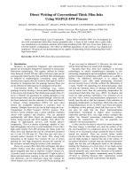
direct writing of conventional thick film inks using maple dw process
Bạn đang xem bản rút gọn của tài liệu. Xem và tải ngay bản đầy đủ của tài liệu tại đây (225.27 KB, 5 trang )
JLMN- Journal of Laser Micro/Nanoengineering, Vol. 1, No. 1, 2006
Direct Writing of Conventional Thick Film Inks
Using MAPLE-DW Process
Edward C. KINZEL, Xianfan XU
*
, Brent R. LEWIS, Normand M. LAURENDEAU and Robert P. LUCHT
School of Mechanical Engineering, Purdue University, West Lafayette, Indiana, 47906 USA
*
E-mail: Phone (765) 494-5639:
Matrix Assisted Pulsed Laser Evaporation – Direct Write (MAPLE-DW) was investigated for
use with conventional thick-film (screen printable) inks. A layer of ink, coated onto a glass slide,
was transferred to an alumina substrate after being irradiated with 1047-nm, 20-ns laser pulses in a
forward transfer configuration. The effect of different parameters on this process was studied and
optimized. The process was demonstrated to be capable of depositing 20-µm conducting lines with a
high linear speed.
Keywords: MAPLE-DW, thick-film, microelectronics
1. Introduction
Increases in operational frequency and interconnect
density are driving the demand for inexpensive mesoscopic
fabrication technologies. This regime, defined by feature
sizes between 10 and 100 µm, falls in between what can be
economically fabricated by thin and thick film technologies.
In addition to morphological constraints, many hybrid
microcircuits require that the resistive and high-Q reactive
elements be integrated into the package because these can
not be effectively fabricated on an integrated circuit (IC).
Conventional thick film technology (e.g., screen
printing) involves forcing a viscous paste through apertures
in the screen and produces film thicknesses greater than 2.5
µm [1]. Patterns are generated by sealing apertures in the
mesh except where ink can be passed through. After the ink
has been patterned onto the substrate it is dried and fired in
a furnace. Firing temperatures (850°C for most inks)
restrict the acceptable substrates to ceramics such as
alumina. Multiple layer devices can be built using the Low-
Temperature Co-fired Ceramic (LTCC) process. This
involves screen printing onto a green substrate (alumina
mixed with organics and binders). Vias are punched
mechanically and these layers are stacked and aligned
before being pressed and fired together. This allows the
design of high-density devices with buried passive
components. This is a mature technology capable of very
high throughputs, but it has several limitations. Even with a
high mesh number (325-400 openings per linear inch), the
finest lines and spacing that can be consistently produced
are 3-5 mil (75-100 µm) [1]. Thin lines may also have a
serrated pattern because of the mesh. This, along with
limitations in the feature size, restricts the use of screen
printing for very high frequencies because the majority of
the current is carried along the surface of the conductor.
There are several other thick-film techniques that have
smaller feature sizes than screen printing. This includes
photo-imagable inks such as DuPont’s Fodel™ system [1].
A positive mask is used with collimated UV light to drive a
photo-polymerization reaction in the ink. Both conductors
and dielectrics can be fabricated using this method, by
which feature sizes down to 25 µm with 50 µm spacing and
75 µm vias may be obtained [1]. However, the inks must
still be fired and there are issues with shrinkage.
Recently there have been new initiatives to develop
technologies to satisfy morphological demands at low
processing temperatures and on nonplanar substrates [2]. A
typical example is metallizing a GPS antenna on a soldier’s
helmet. An additional motivation is to reduce the
development cycle with rapid prototyping electronic
devices directly from CAD files without the fabrication of
a mask. Neither the patterning nor functionalization steps
can heat the substrate above its damage threshold, which
can be much lower than the processing temperature for
conventional thick-film inks (e.g., 400°C for Kapton and
lower for other polymer substrates). Two solutions are to
use inks with a lower functionalization temperature or to
locally heat the ink so that the exposure of the substrate to
damaging temperatures is minimized. Thick-film inks with
firing temperatures as low as 500°C have been developed.
In addition, air-dry polymer based inks that cure at 150°C
can also be used, but the lower functionalization
temperatures correspond to higher sheet resistances.
Nanoscale particles have very high surface energies that
reduce the thermal processing requirements without
reducing the conductivity, but they are generally too
expensive for mass production.
A laser can also be used to selectively sinter the pattern.
The laser energy is absorbed very near the surface of the
ink and transferred via conduction down to the substrate.
Chrisey et al. [3] propose using a pulsed IR laser to locally
anneal the material. There are several failure modes
involved with the laser sintering process. The laser power
may be high enough to vaporize the ink at the surface. If
the pattern thickness is greater than the thermal penetration
depth, the ink may not adequately bond to the substrate,
limiting the thickness of a given layer. If too much power
reaches the substrate, it will become damaged. High
thermal gradients may cause stress fractures in the pattern.
Most importantly, all organic components must be driven
off prior to sintering because their vaporization would
produce high pressures that could destroy the pattern.
74
JLMN- Journal of Laser Micro/Nanoengineering, Vol. 1, No. 1, 2006
Several patterning technologies that satisfy these
requirements include ink-jet based printing [4], Selective
Laser Sintering (SLS), Laser-Induced Forward Transfer
(LIFT), Laser micro-cladding, MicroPen, and Matrix-
Assisted Pulsed Laser Evaporation-Direct Write (MAPLE-
DW). These technologies are discussed in detail in [2].
MAPLE-DW has several advantages over competing
technologies for microelectronics fabrication. First, it is
capable of depositing small feature and requires much
lower laser fluences than either SLS or LIFT. Unlike the
MicroPen, Laser micro-cladding, or ink-jet technologies
MAPLE-DW is also scalable because a common
technology platform can be used for both rapid prototyping
and mass manufacturing by using a mask. The
development of digital light processing (DLP) gives the
potential for a mask-free parallel process. Like ink-jet
printing and the MicroPen, MAPLE-DW is capable of
depositing virtually any type of material, including
chemicals and biological samples which are important for
developing sensors and batteries [2]. In MAPLE-DW, the
ribbon, which is a supporting substrate with a layer of
material to be coated (ink), is placed in close proximity
(25-100 µm) to another substrate where the material needs
to be deposited in the forward transfer configuration. A
laser is focused through the transparent support onto the
ink-support interface. The ink absorbs the laser radiation
and is rapidly heated and vaporized. This provides a
pressure pulse which pushes the fluid material outward and
deposits it onto the substrate. The substrate can be
translated relative to the laser to create very precise
patterns. The entire process takes place in ambient
conditions and does not require heating of the substrate. In
addition when the ribbon is removed, the same laser system
that is used to write the pattern can also be used for laser
trimming of the components (direct erase), or surface
modification such as cutting vias. A sintering laser is also
easy to integrate with MAPLE for in situ sintering.
This paper investigates the implementation of MAPLE-
DW using conventional microelectronic inks with an IR
laser and X-Y scanner for high-speed writing. Previous
investigations have used either Excimer or frequency-
tripled Nd:YAG lasers, which both produce UV
wavelengths [2,3,5,6]. Using IR wavelengths is more
convenient because glass supports can be used. In addition,
if an IR laser is to be used to sinter the material after
deposition, the same optical system can be used for both
the patterning and functionalization processes. We focus on
creating conductors with QS300. This is a Ag/Pt
conductive ink manufactured by Dupont and specifically
developed for the screen printing industry. It is widely
available and has been designed for producing fine lines
down to 75 µm using screen-printing. QS300 has a
specified sheet resistance of 4.5 mΩ/square for a fired film
thickness of 10 µm at 850°C. The rheology of screen
printing inks is specifically designed to vary with the shear
force applied to the ink. In the absence of shear forces, the
ink is very viscous. This helps deposited patterns resist
distortions once they are on the substrate.
2. Experimental
Figure 1 shows a schematic of our experimental setup.
An X-Y scanner moves the laser beam according to a
computer-controlled path relative to a fixed substrate. This
offers higher write speeds than translation stages would
otherwise allow. The ribbon and substrate are both
stationary. The Nd:YLF laser produces 20-ns pulses at a
given pulse repetition frequency (PRF) and a wavelength of
1047 nm. The PRF of this laser can be varied from
continuous wave (CW) to 10 kHz. By expanding the beam,
a waist of ~16 µm can be achieved at the focal plane. The
size of the mirrors on the X-Y scanner limits the diameter
to which the beam may be expanded to ~1 inch. Shot-to-
shot spacing is controlled by adjusting PRF and the speed
of the X-Y scanner. A CCD camera allows the substrate to
be positioned using the x-y stages as well as monitoring the
process in situ. A CW JDSU fiber laser (λ = 1100 nm) can
be used to sinter the patterns deposited by MAPLE-DW.
The two lasers are aligned so that they have the same
optical path through the system.
Fig 1. Schematic of setup for MAPLE-DW
The MAPLE-DW process has been previously
investigated with time-resolved microscopy by Young et al
[5]. They identified three different operational regimes for
the MAPLE-DW process: sub-threshold, jetting, and plume,
in order of increasing laser fluence. The ink they
investigated consisted of BaTiO
3
nanopowder in a α-
terpineol matrix with a small amount of surfactants.
A photography experiment was also conducted in the
present work using the configuration in Fig. 1. The QS300
was mixed with 11% (by mass) α-terpineol. Three regions
are also identified, named bubble protrusion regime, jetting
and plume, and are correlated with the results of quality of
MAPLE-DW process. Examples of these three regimes
from our experiment are shown in Fig. 2.
All three responses begin with the protrusion of a
bubble from the surface of the ink. The bubble protrusion
regime is characterized by an expanding bubble that never
fully detaches from the ink surface The bubble eventually
collapses back into the ink surface because its kinetic
energy is insufficient to overcome surface tension. A jet is
formed when the energy is large enough to overcome
surface tension and at least some of the ink is detached
from the surface. Surface tension then causes this ink to
collapse in the radial direction. The plume regime is similar
to the jet except that the ink leaves the surface with a high
Nd:YLF Laser
Mirror
Ad
j
ustable Polarizer
Beam Ex
p
anders
X-Y Scanner
Com
p
uter
T
V Monitor
CCD Camera
Hot Mirror
IR Filter
Z-Sta
g
e
X-Sta
g
e
Y-Sta
g
e
Substrate
Ribbon
Fiber Laser
Mirror
Flip Mirror
75
JLMN- Journal of Laser Micro/Nanoengineering, Vol. 1, No. 1, 2006
enough velocity that it breaks into small droplets and
continues to expand radially as well as normally to the
surface.
(a) (b) (c)
Fig. 2. Micrographs of different response regimes
(a) sub-threshold – 0.79 J/cm
2
(b) jetting 1.02 J/cm
2
and (c) plume – 1.27 J/cm
2
.
Working in the jetting regime is appealing because the
ink collapses to a smaller diameter than the laser spot.
However, considerable instability was observed in the jets
and the ink splatters when it comes in contact with the
substrate due to the high velocity of the jet. Both of these
effects ultimately limit the feature size. Zhang et al [6] used
the plume regime with a dried ribbon in direct contact with
the substrate. Because the ribbon is dried, it is more
suitable for storage and more applicable for printing on
conformal substrates. Since the ribbon is in contact with the
substrate, radial spreading is minimized when a laser with a
small spot size is used with a thin ink layer. However, there
can be problems with producing dense unbroken patterns
because the deposited ink has a smaller diameter, and
therefore is not continuous. Zhang et al used wet ribbons
for depositing dielectrics to avoid pinholing [6].
The remaining experiments in this paper use QS300
without the addition of any thinner and operate in the sub-
threshold regime. Ink was applied to the glass substrate
using a glass rod and steel shims because the unadulterated
QS300 is too viscous for the use of a wire or spin coater.
The thickness of the ink layer can be controlled by using
different sets of shims. Time histories of the MAPLE-DW
event were captured using high-speed microscopy for 0.5-,
1.0-, and 2.0-mil ink layer thicknesses, with beam waists of
15 and 30 µm. These experiments showed that as laser
fluence is increased, the size of the bubble increases until it
ruptures into a plume. For the range of film thicknesses,
beam radii, and spot sizes there is no fluence that produces
a jet. The maximum bubble displacement for each
experiment is graphed in Figure 3. The range of laser
fluences was selected to span the range of sub-threshold
regime. A correlation was developed that captures the
general trends of the experiment.
2
61.31
0
max
0.5
1.35 10
−
=×⋅⋅
r
zF
d
(1)
where z
max
is the maximum displacement of the bubble in
µm, F is the laser fluence in J/m
2
, r
0
is the beam radius at
the ink-support interface in µm, and d is the ink thickness
in µm. An analytical correlation between the maximum
displacement and the processing parameters is currently
being developed.
It is seen from Fig. 3 and Eq. (1) that the maximum
displacement of the bubble increases with laser fluence. A
larger beam radius pushes the bubble out farther for the
same fluence. It also requires more laser fluence to displace
a thicker ink layer a given distance than a thinner layer.
Considering the micrograph of the sub-threshold response
in Fig. 1(a), a bubble with a larger base radius will have
lower curvature for a given displacement than a bubble
with a smaller radius. The stress in the bubble walls due to
surface tension will be proportional to this curvature.
Above a certain threshold for the material and thickness the
bubble wall will fail and MAPLE-DW moves into the
plume regime.
0
10
20
30
40
50
60
70
80
0 10000 20000 30000
Laser flunce [J/m
2
]
Maximum displacement [µm]
0.0005" - 15 µm
0.0010" - 15 µm
0.0020" - 15 µm
0.0005" - 30 µm
0.0010" - 30 µm
0.0020" - 30 µm
d - r
0
Fig. 3. Maximum displacement as a function of laser fluence. The
lines show the correlation in Eq. 1.
0.0
0.2
0.4
0.6
0.8
1.0
1.2
1.4
1.6
0 10000 20000 30000
Laser fluence [J/m
2
]
z
max
/R
0
0.0005" - 15 µm
0.0010" - 15 µm
0.0020" - 15 µm
0.0005" - 30 µm
0.0010" - 30 µm
0.0020" - 30 µm
d - r
0
Fig. 4. Ratio of maximum displacement to base radius as a
function of laser fluence.
Because of the thixotropy of the ink, there will be
effective plastic deformation of the bubble and it will not
return to the surface for all but the lowest laser fluences.
Because the ribbon is not moving for the setup used in this
paper, this can be a great impediment to writing thin lines.
The best experimental results are obtained when the ribbon
is positioned as close to the substrate as possible and the
majority of the displaced ink is deposited. The interaction
between the ink and the substrate is also important, and
how well the ink wets the substrate can play a critical role
in the morphology of the final pattern. Alumina slides
76
JLMN- Journal of Laser Micro/Nanoengineering, Vol. 1, No. 1, 2006
coated with a dielectric (Dupont QM44) were used in this
work. These substrates have some surface roughness and
appear to draw the ink downward and hold it to form fine
patterns.
It is convenient to define a quality factor for the sub-
threshold event to help quantify the shot to shot
interference on the ribbon. The ratio of maximum
displacement to the base radius is plotted in Fig. 4 for the
same experimental cases as in Fig. 3. The most deposition
should occur for bubbles that have a maximum
displacement while maintaining a minimum base radius.
Fig. 4 shows that this is true for the larger beam radii and
lower ink thicknesses.
Figure 5 shows micrographs of the deposited patterns
with respect to laser fluence. The lines in the figure were
written at 7 cm/s. The separation between the ink and the
substrate is ~ 12.5 µm. Figure 6 shows a portion of a 20 µm
wide, 5 mm long wire printed with 1.26 J/cm
2
. This line
was fired in a furnace at 850°C. The conductivity was
measured to be 1.6 × 10
7
1/Ω·m, or ~75% of the specified
value for QS300. This small reduction is most likely due to
inconsistencies in the line dimensions and porosity in the
fired material.
2.99 J/cm
2
2.71 J/cm
2
2.54 J/cm
2
2.35 J/cm
2
2.13 J/cm
2
1.65 J/cm
2
Fig. 5. Deposition on alumina substrate for various fluences.
Fig. 6. Micrographs of a 20-µm line
The MAPLE-DW process is very sensitive to the
thickness of the ink layer and the separation between the
substrate and the ink layer. Using shims to coat the ribbons
and separate the substrates makes it difficult to control
these parameters precisely across the entire surface of the
substrate. The narrowest line obtained in this work is about
10 µm wide. Smaller lines with smother edges can be
obtained by ablating the edges of the lines.
When the lines are deposited onto the substrate the
material still has the same properties as the ink on the
ribbon. Because there is a substantial amount of organic
material in the deposited pattern, it is difficult to sinter the
pattern in situ. The fiber laser was also employed to sinter
the ink, which was uniformly coated on the substrate and
then dried in a convection oven at 150°C. QS300 has been
successfully sintered on soda-lime glass (T
g
~550°C) to
produce a conductance that is nearly identical to what is
specified for the ink.
MAPLE-DW provides a maskless way to rapid
prototype thick film mesoscopic features. The speed of the
X-Y scanner may be sufficient for low production runs. If
higher throughputs are required, a negative mask can be
deposited on the ribbon and the entire pattern deposited
with one laser pulse.
3. Conclusions
This paper has demonstrated that conventional screen
printable inks can be used with MAPLE-DW using an
infrared pulsed laser. The best lines are obtained in the sub-
threshold regime when bubbles collapse back to the glass
substrate. In addition, an X-Y scanner can also be used to
rapidly write the patterns at very high write speeds.
Features as small as 10 µm can be written. With higher
precision coating and substrate ribbon separation, the
quality and consistency of the patterns could be greatly
improved.
Acknowledgments and Appendixes
The authors wish to gratefully acknowledge the State of
Indiana’s 21
st
Century Research and Development Fund for
supporting this work and Carl Berlin at Delphi Delco
Automobile Electronics for providing the materials used in
this work. E.C.K. and B.R.L. also thank the Lozar
Fellowship of the School of Mechanical Engineering,
Purdue University.
References
[1] J.J. Licari and L.R. Enlow: “Hybrid Microcircuit
Technology Handbook (2
nd
Ed.)” William Andrew
Publishing, 1998
[2] A. Piqué and D.B. Chisey: “Direct-Write Technologies
for Rapid Prototyping Applications: Sensors,
Electronics, and Integrated Power Sources”, Academic
Press, San Diego, (2002)
[3] D.B. Chrisey, A. Piqué, R. Modi, H.D. Wu, R.C.Y.
Auyeung, and H.D. Young: Applied Surface Science,
168 (2000)
[4] D. Redinger, S. Molesa, S. Yin, R. Farschi, and V.
Subramanian: IEEE Transactions on Electron Devices,
51-12, (2004)
140 µm
70 µm
100 µm
50 µm 40 µm 20 µm
20 µm
20 µm
77
JLMN- Journal of Laser Micro/Nanoengineering, Vol. 1, No. 1, 2006
[5] D. Young, R.C.Y. Auyeung, A. Piqué, D.B. Chrisey,
and D.D. Dlott: Applied Surface Science, 197-198
(2002)
[6] C. Zhang, D. Liu, S.A. Mathews, J. Graves, T.M.
Schaefer, B.K. Gilbert, R. Modi, H. Wu, and D.B.
Chrisey: Microelectronic Engineering, 70 (2003) 41-49
(Received: April 5, 2005, Accepted: November 22, 2005)
78