mechanism of vertical ge nanowire nucleation on si (111) during subeutectic annealing and growth
Bạn đang xem bản rút gọn của tài liệu. Xem và tải ngay bản đầy đủ của tài liệu tại đây (151.36 KB, 5 trang )
Mechanism of vertical Ge nanowire nucleation on Si (111) during
subeutectic annealing and growth
Se Jun Park
a)
Birck Nanotechnology Center, Purdue University, West Lafayette, Indiana 47907; and School of Mechanical
Engineering, Purdue University, West Lafayette, Indiana 47907
Sung Hwan Chung
Birck Nanotechnology Center, Purdue University, West Lafayette, Indiana 47907; and School of Electrical and
Computer Engineering, Purdue University, West Lafayette, Indiana 47907
Bong-Joong Kim
b)
Birck Nanotechnology Center, Purdue University, West Lafayette, Indiana 47907; and School of Materials
Engineering, Purdue University, West Lafayette, Indiana 47907
Minghao Qi
Birck Nanotechnology Center, Purdue University, West Lafayette, Indiana 47907; and School of Electrical and
Computer Engineering, Purdue University, West Lafayette, Indiana 47907
Xianfan Xu
Birck Nanotechnology Center, Purdue University, West Lafayette, Indiana 47907; and School of Mechanical
Engineering, Purdue University, West Lafayette, Indiana 47907
Eric A. Stach
b)
Birck Nanotechnology Center, Purdue University, West Lafayette, Indiana 47907; and School of Materials
Engineering, Purdue University, West Lafayette, Indiana 47907
Chen Yang
c)
Department of Chemistry, Purdue University, West Lafayette, Indiana 47907; and Department of Physics,
Purdue University, West Lafayette, Indiana 47907
(Received 11 April 2011; accepted 19 August 2011)
The direct integration of Ge nanowires with silicon is of interest in multiple applications. In this
work, we describe the growth of high-quality, vertically oriented Ge nanowires on Si (111)
substrates utilizing a completely sub-Au–Si-eutectic annealing and growth procedure. With all other
conditions remaining identical, annealing below the Au–Si eutectic results in successful
heteroepitaxial nucleation and growth of Ge nanowires on Si substrate while annealing above the
Au–Si eutectic leads to randomly oriented growth. A model is presented to elucidate the effect of the
annealing temperature, in which we hypothesized that sub-Au–Si-eutectic annealing leads to
the formation of a single and well-oriented interface, essential to template heteroepitaxial nucleation.
These results are critically dependent on substrate preparation and lead to the creation of integrated
nanowire systems with a low thermal budget process.
I. INTRODUCTION
Semiconductor nanowires have attracted substantial
interest in recent years due to their wide range of potential
applications, including nanoelectronics, thermoelectrics,
solar energy conversion, and biosensing.
1–5
Germanium
nanowires are of particular interest for their high intrinsic
hole and electron mobilities when compared to silicon,
6,7
relatively low-growth temperature (below 400 °C), and
compatibility with current silicon VLSI technology.
The widely accepted growth mechanism for the creation
of Ge nanowires is the vapor–liquid–solid (VLS) mecha-
nism. During VLS nanowire growth, a vapor phase
precursor for Ge—such as GeH
4
or Ge
2
H
6
—decomposes
catalytically at the surface of a metal nanoparticle (most
often one with which it forms a binary eutectic) and then
dissolves into the metal nanoparticle to form a molten alloy.
The continuous supply of Ge from the vapor phase results i n
supersaturation of Ge within the liquid alloy nanoparticle,
and l eads first t o nucleation and then axial g rowth of t he
nanowire. P roper e pitaxial growth requires that the initial
nucleation event occurs via the formation of an epitaxial
interface with the substrate, which provides the template by
which the nanowire selects its growth directio n.
a)
Current address: Semiconductor Division, Samsung Electronics
Co. Ltd., Gyeonggido, South Korea
b)
Current address: Center for Functional Nanomaterials, Brookhaven
National Laboratory, Upton, New York 11973
c)
Address all correspondence to this author.
e-mail:
DOI: 10.1557/jmr.2011.313
J. Mater. Res., Vol. 26, No. 21, Nov 14, 2011 Ó Materials Research Society 20112744
Conceptually, the formation of liquid alloy droplets
requires that the growth process be carried out at temper-
atures above the binary eutectic melting point, 361 °C in
the case of Au–Ge studied here. Recently, several studies
have shined the light in the mechanism of VLS Ge nano-
wire growth below the Au–Ge eutectic point.
8–10
McIntyre
et al. postulated that the liquid can be stabilized below the
eutectic temperature by two phenomena: first the barrier
associated with homogeneous nucleation of solid Au, and
second the excess saturation of Ge required to drive the
transfer of Ge atoms from the liquid droplet to the growing
solid nanowire.
9
Growth via the VLS mode below the
eutectic temperature was confirmed via direct observations
in the work of Kodambaka et al.
8
These observations are
important because the ability to grow uniform epitaxial Ge
nanowires at low-growth temperatures is of strong interest,
enabling a decrease in the overall thermal budget during
semiconductor device processing.
Heteroepitaxial integration of Ge nanowires on Si
substrates is of particular interest as this offers a direct,
bottom-up assembly approach with control of orienta-
tions and compatibility with current silicon-based industrial
manufacturing processes. A two-step strategy is commonly
utilized. Either a n ucleation step with Ge p recursor pro-
vided or an annealing step without the pr ese nce of Ge
precursor is performed typically at a temperature different
from the growth temperature before the growth step. To
achieve reproducible epitaxial growth, numerous factors,
such as substrate preparation, growth temperature, total
pressure, partial pressure of the reactive gas, and metal
catalyze size, need to be optimized.
11–16
For example, the
underlying substrate orientation influences the crystallo-
graphic orientation of the epitaxially grown nanowires.
Generally, the highest quality Ge nanowires are grown on
(111) oriented substrates, with Au catalysts larger than
20 nm, and result in ,111. oriented, single crystalline
nanowires which grow vertically from the substrate.
Moreover, growth quality can be affected by the annealing
of the substrate prior to growth.
12,14
In prior work, high
temperature annealing (above Au–Si eutectic point) of the
substrate prior to the introduction of the gas precursor has
been found to facilitate a high density of epitaxial Ge
nanowires grown ranging between 320 and 380 °C.
Kamins et al.
12
suggested that this annealing step removes
any residual solvent and thereby improves the contact of
the Au nanoparticles with the Si substrates, which prob-
ably enhances the ability of the nanowires to template
epitaxially at the onset of nucleation.
In this work, we demonstrate the growth of dense,
epitaxial Ge nanowires on a (111) silicon substrate using
annealing and growth steps both carried out at as low as
280 °C. These results allow us to form high-quality Ge
nanowires on silicon with a further low-thermal budget
process, a substantial improvement towards incorporation
into conventional VLSI processing.
II. EXPERIMENTAL SECTION
Prior to growth, the substrate was etched with a buff-
ered hydrofluoric acid solution to remove the surface
oxide. A well-mixed solution containing 200llof40nm
gold colloidal nanoparticles and 2 ml of 10% HF/H
2
O
15
was then dispersed on the substrate. The substrate was
then rinsed, dried, and loaded in a chemical vapor de-
position system. The substrates were annealed between
280 to 400 °C for 5 min in 100 Torr of flowing H
2
. The
time between the particle deposition and the onset of
annealing was of the order of 10 min and was crucial to
successful nanowire growth. Immediately after the anneal-
ing, Ge nanowire growth was carried out using 10 sccm of
GeH
4
(5% diluted in H
2
) and 40 sccm of H
2
at a total
pressure of 100 Torr an d a substrate temperature of 280 °C.
This growth temperature was chosen because it was the
minimum growth temperature at which nanowire growth
could be achieved, as determined by systematically in-
creasing the temperature from 265 °C. To investigate the
effect of annealing, all Ge nanowires were grown in the
same conditions, following only a variation in the annealing
temperatures.
III. RESULTS AND DISCUSSION
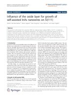
Figures 1(a) and 1(b) present scanning electron micros-
copy (SEM) images of Ge nanowires grown on a Si (111)
substrate using annealing temperatures of 280 and 320 °C,
respectively. The results are essentially the same for
both conditions. The nanowires show uniform diameters
without significant tapering along an average length of
;2.2 lm. Significantly, a majority of nanowires are found
to be oriented perpendicular to the substrate,
indicating epitaxial growth along the ,111. growth
direction. Additionally, a small fraction of nanowires
which grew along other ,111. directions were also
observed: these as nanowires present at an angle of
approximately 70° to the substrate normal in a cross-
sectional view and have an angle of 120° between them
when projected in plan-view.
14
Figures 1(d)–1(f) present
transmission electron microscopy analysis of the Ge nano-
wires grown following annealing at 320 °C. These images
confirm that the Ge nanowires are defect free over their
entire length. The inset electron diffraction pattern—taken
along the
112
fg
zone-axis o rientation—indicates a ,111.
growth direction, consis tent with the g rowth direction
observed from SEM images. Collectively, these results
demonstrate that Ge n anowires are heteroepitaxially grown
on a Si (111) substrate successfully with both annealing and
growth at deep subeutectic temperatures. In contrast, when
the substrate was annealed above t he eutectic temperature of
363 °C for Au–Si, in our case 400 °C, there was no
successful nanowire growth, as shown in Fig. 1(c). This
comparison suggests th at an a nnealing temperature below
S.J. Park et al.: Mechanism of vertical Ge nanowire nucleation on Si (111) during subeutectic annealing and growth
J. Mater. Res., Vol. 26, No. 21, Nov 14, 2011 2745
the Au–Si eutectic temperature is critical for successful
epitaxial growth of Ge nanowires on S i (111) substrates at
a growth temperature of 280 °C.
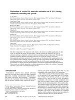
Figure 2 illustrates our explanation of the mechanism by
which annealing affects nanowire nucleation a nd the selec-
tion of nanowir e orientation. It is known that the p recleaning
of Si s ubstrates with buffered HF not only removes the
native oxide bu t also c reates a h ydrogen-terminated surface
that is stable in air for several minutes.
17
We postulate that
the combination of substrate precleaning in buffered HF and
the deposition of the colloidal Au nanoparticles i n a dilute
HF solution leads to intimate contact between the Au par-
ticles and the growth substrate in addition to enhanced
deposition of Au colloid particles and removal of native
oxide.
15
During subsequent annealing below the Au–Si
eutectic temperature [ Fig. 2(a)], one would expect very little
reaction between the solid Au and the Si substrate, as Au is
nearly insoluble t o S i below the eutectic temperature, based
on the equilibrium phase diagram. However, this low
temperature anneal m ust be leading to the formation of
a well-defined, homogeneous and planar ,111. oriented
interface between the Au solid and the Si substrate prior to
introduction of the Ge growth precursor. This allows proper
templating for the s ubsequent Ge nanowire nucleation event,
consistent with our observations of predominantly vertically
oriented nanowires. In comparison, annealing above the
eutectic temperature (e.g., 400 °C) will result in the for-
mation of a Au–Si eutectic liquid alloy (with approximately
19% Si), which develops facets below the substrate surfaces
[the so-called “alloy-in” effect—Fig. 2(b)].
18,19
Upon sub-
sequent lowering of the temperature below the eutectic
temperature for growth (280 °C), a significantamountofSi
will be rejected to the s ubstrate during solidification, pre-
sumably templating onto the facets formed during anneal-
ing. Subsequent p rovision o f Ge to the now-solidified Au–Si
droplet via the GeH
4
precursor will result in nanowire
nucleation with growth observed in arbitrary directions
because of the nonuniform n ature of the catalyst/substrate
interface.
To confirm the critical role of a well-formed Au–Si
interface prior to subeutectic Ge nanowire growth, we
replicated these growth studies on substrates with a thick
surface oxide (600 nm). Although presence of the oxide
prevents the formation of Au–Si alloy during annealing
above the eutectic temperature, the oxide will prevent the
FIG. 1. Scanning electron microscopy (SEM) and high-resolution transmission electron microscopy (HRTEM) images of Ge nanowires grown on Si
(111). Growth was carried out at 280 °C, with annealing at (a) 280, (b) 320, and (c) 400 °C. SEM images were taken with a 25° inclination from the
plan-view (in a, b, and c) and in cross-sectional view (insets to a, b, and c). Scale bars are 5 lm in (a)–(c) and 2 lm in (a)–(c) insets. (d) HRTEM image,
(e) bright-field TEM image, and (f) electron diffractogram of a Ge nanowire produced following annealing at 320 °C. Scale bars are 2 and 100 nm in
(d) and (e), respectively.
FIG. 2. Schematic illustration of the mechanism of Ge nucleation and
growth on Si following annealing (a) below and (b) above the Au–Si
eutectic temperature.
S.J. Park et al.: Mechanism of vertical Ge nanowire nucleation on Si (111) during subeutectic annealing and growth
J. Mater. Res., Vol. 26, No. 21, Nov 14, 20112746
formation of a ,111. Au/Si interface. As expected,
similar results were observed following annealing both
below and above the Au–Si eutectic temperature (Supple-
mental Information). The orientation of the Ge nanowires
was found to be random, clearly indicating the failure of
heteroepitaxial templating.
The improved understanding of the fundamental mech-
anisms of low temperature nanowire growth can be used
to create novel and potentially useful structures. As shown
in Fig. 3, we can utilize this same approach to growth
nanowires in-plane. Si microtrenches with exposed {111}
planes were fabricated following the method developed by
He et al.
20,21
Heteroepitaxial growth of Ge nanowires in
a ,111. direction from the sidewalls of these trenches was
achieved utilizing a 280 °C growth, following a 280 °C
annealing, completely bridging the trench and leading to
intimate contact (as determined via electrical measure-
ments, not shown). These results demonstrate that this
growth approach provides a nanowire device fabrication
method requiring a low thermal budget and yet potentially
offering the superior electronic properties of germanium.
IV. CONCLUSIONS
In summary, our work demonstrates that it is possible
to grow vertical, integrated Ge nanowires on silicon
substrates with a two-step process, including annealing
and growth, both at temperature of 280 °C, lower than
previously reported. This is based on the creation of
a single, ordered ,111. interface between the Au and
the Si, prior to Ge introduction. This work indicates that
careful but relatively simple control of both substrate
preparation and annealing and growth procedures can lead to
heteroepitaxial growth of oriented, single crystalline Ge
nanowires on Si completely below the e utectic temperature,
with important ramifications for device creation.
ACKNOWLEDGMENT
The work was supported by the Defense Advanced
Research Project Agency award N66001-08-1-2037. S. J. P.
thanks the support by the Korean Research Foundation
Grant funded by the Korean Governmen t (KRF-200 7-357-
D00022).
REFERENCES
1. Y. Li, F. Qian, J. Xiang, and C.M. Lieber: Nanowire electronic and
optoelectronic devices. Mater. Today 9, 18 (2006).
2. A.I. Hochbaum, R. Chen, R.D. Delgado, W. Liang, E.C. Garnett,
M. Najarian, A. Majumdar, and P. Yang: Enhanced thermoelectric
performance of rough silicon nanowires. Nature 451, 163 (2008).
3. A.I. Boukai, Y. Bunimovich, J. Tahir-Kheli, J-K. Yu, W.A. Goddard,
and J.R. Heath: Silicon nanowires as efficient thermoelectric
materials. Nature 451, 168 (2008).
4. K-Q Peng and S-T Lee: Silicon nanowires for photovoltaic solar
energy conversion. Adv. Mater. 23, 198 (2011).
5. F. Patolsky, G. Zheng, and C.M. Lieber: Nanowire-based biosen-
sors. Anal. Chem. 78, 4260 (2006).
6. D. Wang, Q. Wang, A. Javey, R. Tu, H. Dai, H. Kim, P.C. McIntyre,
T. Krishnamohan, and K.C. Saraswat: Germanium nanowire field-
effect transistors with SiO
2
and high-j HfO
2
gate dielectrics.
Appl. Phys. Lett. 83, 2432 (2003).
7. A.B. Greytak, L.J. Lauhon, M.S. Gudiksen, and C.M. Lieber:
Growth and transport properties of complementary germanium
nanowire field-effect transistors. Appl. Phys. Lett. 84, 4176 (2004).
8. S. Kodambaka, J. Tersoff, M.C. Reuter, and F.M. Ross: Germanium
nanowire growth below the eutectic temperature. Science 316, 729
(2007).
9. H. Adhikari, P.C. McIntyre, A.F. Marshall, and C.E.D. Chidsey:
Conditions for subeutectic growth of Ge nanowires by the vapor-
liquid-solid mechanism. J. Appl. Phys. 102, 094311 (2007).
10. A.D. Gamalski, J. Tersoff, R. Sharma, C. Ducatiand, and S. Hofmann:
Formation of metastable liquid catalyst during subeutectic growth of
germanium nanowires. Nano Lett. 10,2972(2010).
11. P.C. McIntyre, H. Adhikari, I.A. Goldthorpe, S. Hu, P.W. Leu,
A.F. Marshall, and C.E.D. Chidsey: Group IV semiconductor nano-
wire arrays: Epitaxy in different contexts. Semicond. Sci. Technol.
25, 024016 (2010).
12. T.I. Kamins, X. Li, R.S. Willians, and X. Liu: Growth and structure
of chemically vapor deposited Ge nanowires on Si substrates. Nano
Lett. 4, 503 (2004).
13. J.W. Dailey, J. Taraci, T. Clement, D.J. Smith, J. Drucker, and
S.T. Picraux: Vapor-liquid-solid growth of germanium nanostructures
on silicon. J. Appl. P hys. 96, 7556 (2004).
14. H. Jagannathan, M. Deal, Y. Nishi, J. Woodruff, C. Chidsey, and
P.C. McIntyre: Nature of germanium nanowire heteroepitaxy on
silicon substrates. J. Appl. Phys. 100, 024318 (2006).
15. J.H. Woodruff, J.B. Ratchford, I.A. Goldthorpe, P.C. McIntyre, and
C.E.D. Chidsey: Vertically oriented germanium nanowires grown
from gold colloids on silicon substrates and subsequent gold
removal. Nano Lett. 7, 1637 (2007).
16. P. Manandhar, E.A. Akhadov, C. Tracy, and S.T. Picraux: In-
tegration of nanowire devices in out-of-plane geometry. Nano Lett.
10, 2126 (2010).
17. G.S. Higashi, Y.J. Chabal, G.W. Trucks, and K. Raghavachari:
Ideal hydrogen termination of the Si (111) surface. Appl. Phys. Lett.
56, 656 (1990).
18. N. Ferralis, R. Maboudian, and C. Carraro: Temperature-Induced
self-pinning and nanolayering of AuSi eutectic droplets.
J. Am. Chem. Soc. 130, 2681 (2008).
19. U. Krishnamachari, M. Borgstrom, B.J. Ohlsson, N. Panev,
L. Samuelson, W. Seifert, M.W. Larsson, and L.R. Wallenberg:
Defect-free InP nanowires grown in [001] direction on InP (001).
Appl. Phys. Lett. 85, 2077 (2004).
FIG. 3. SEM image of a Ge nanowire grown across a Si trench
structure. Scale bar is 1 lm.
S.J. Park et al.: Mechanism of vertical Ge nanowire nucleation on Si (111) during subeutectic annealing and growth
J. Mater. Res., Vol. 26, No. 21, Nov 14, 2011 2747
20. M.S. Islam, S. Sharma, T.I. Kamins, and R.S. Williams: Ultrahigh-
density silicon nanobridges formed between two vertical silicon
surfaces. Nanotechnology 15, L5 (2004).
21. R. He, D. Gao, R. Fan, A.I. Hochbaum, C. Carraro, R. Maboudian,
and P. Yang: Si nanowire bridges in microtrenches: Integration of
growth into device fabrication. Adv. Mater. 17, 2098 (2005).
Supplementary Mater ial
Supplementary material can be viewed in this issue of the Journal of Materials Research by visiting
/>S.J. Park et al.: Mechanism of vertical Ge nanowire nucleation on Si (111) during subeutectic annealing and growth
J. Mater. Res., Vol. 26, No. 21, Nov 14, 20112748