- Trang chủ >>
- Khoa Học Tự Nhiên >>
- Vật lý
Effect of tunneling current on the growth of silicon islands on si(111) surfaces with a scanning tunneling microscope
Bạn đang xem bản rút gọn của tài liệu. Xem và tải ngay bản đầy đủ của tài liệu tại đây (261.83 KB, 7 trang )
Surface Science 447 (2000) 149–155
www.elsevier.nl/locate/susc
Effect of tunneling current on the growth of silicon islands on
Si(111) surfaces with a scanning tunneling microscope
Alexander A. Shklyaev 1, Motoshi Shibata, Masakazu Ichikawa
*
Joint Research Center for Atom Technology (JRCAT), Angstrom Technology Partnership (ATP), 1-1-4 Higashi, Tsukuba,
Ibaraki 305-0046, Japan
Received 5 July 1999; accepted for publication 15 November 1999
Abstract
The early-stage growth rate of a silicon island on a Si(111) surface at the center of the interaction between a
sample and the tip of a scanning tunneling microscope (STM ) was defined as a function of the tunneling current.
The tunneling current dependence of the rate has a maximum at 0.3 nA, and the decrease of the rate at tunneling
currents above 0.3 nA was related to the effect of electron flow on atom transfer by field-induced directional diffusion.
The early-stage growth rate was about three times higher than the late-stage growth rate, which was almost
independent of the tunneling current. The results suggest that atom transfer by field-induced diffusion on the sample
surface was gradually substituted by atom transfer from the STM tip by field-induced silicon atom re-evaporation as
the island grew from 0 to about 12 nm in height. © 2000 Elsevier Science B.V. All rights reserved.
Keywords: Diffusion and migration; Field effect; Growth; Scanning tunneling microscopy; Semiconducting surfaces; Silicon; Surface
structure, morphology, roughness, and topography
1. Introduction ostructure by each voltage pulse, and the number
of atoms involved in the transfer cannot be con-
trolled well by the voltage of the pulses or by the
A surface structure can be modified by transfer-
pulse duration [5,6]. We have recently demon-
ring individual atoms and molecules with a scan-
strated that growth of a three-dimensional (3D)
ning tunneling microscope (STM ) [1,2]. Such
silicon island on a Si(111) surface occurs at the
modifications are usually achieved when micro- or
center of the tip–sample interaction after applying
millisecond voltage pulses are applied between the
elevated negative bias voltages (6–10 V ) to the
sample and the STM tip [3,4]. The creation of
STM tip at a constant tunneling current [7]. The
nanostructures, which involves the transfer of hun-
island was created by transferring atoms towards
dreds and thousands of atoms, can be performed
the center from the area around the island.
by increasing the voltage of the pulses [5,6 ].
In this work, in order to outline the conditions
However, in ultrahigh vacuum ( UHV) conditions,
for reproducible island formation, the kinetics of
there is only a probability of producing a nan-
island growth — that is, island height as a function
of the duration of tip–sample interaction — was
* Corresponding author. Fax: +81-298-54-2577.
obtained for various tunneling currents. We deter-
E-mail address: (M. Ichikawa)
mined the early- and late-stage growth rates from
1 On leave from the Institute of Semiconductor Physics,
Novosibirsk 630090, Russia.
these kinetic data. The tunneling current depen-
0039-6028/00/$ - see front matter © 2000 Elsevier Science B.V. All rights reserved.
PII: S0 039- 6 028 ( 99 ) 01165-6
150 A.A. Shklyaev et al. / Surface Science 447 (2000) 149–155
dence of the early-stage growth rate has a sharp current of the voltage pulse destroyed the old tip
apex. There was a probability of achieving a newmaximum at 0.3 nA. Such a dependence reflects
the competition between the effect of the electric tip apex that was sufficiently sharp. To check the
final sharpness of the new tip apex, we createdfield of the STM, which is responsible for direc-
tional diffusion towards the growing island, and silicon islands with the STM and examined the
quality of STM images of the islands. Note thatthe effect of the electron flow, which pushes the
diffusion in the opposite direction. The late-stage after the creation of islands with the STM, the
accumulation of silicon atoms on the tip apex wasgrowth rate was about three times lower than the
early-stage growth rate and was almost indepen- not observed with the SREM. This indicates that
the probable silicon coverage on the tip apex wasdent of the tunneling current and island height.
Analysis of the difference between the rates allowed below 20 nm, which is the limit of SREM
measurements.us to distinguish mechanisms of the early stage
and late stage of island growth. At the late stage,
the transfer of silicon atoms from the STM tip by
re-evaporation of the silicon that was accumulated 3. Results and discussion
on the STM tip at the initial stages of the tip–
sample interaction very likely occurs in the growth The reproducible formation of the 3D silicon
islands on the Si(111) surface with the STM hasof islands over 4 nm in height. Island growth was
not stable at tunneling currents above 1.0 nA. At been observed at small tunneling currents of less
than 0.5 nA. At a given duration of the voltagelarge tunneling currents, a pit or a pit near an
island could appear on the surface. The corre- pulse, the scattering of the island height for islands
grown in one experimental run was within 10%,sponding tip–sample interaction process was
accompanied by fluctuations of the tunneling cur- and the height of islands increased gradually when
the duration increased [7]. Fig. 1 shows STM datarent and mechanical vibrations of the STM tip in
the direction normal to the surface. for the islands grown at a larger tunneling current
of 1.2 nA for various durations of the tip–sample
interaction. At this large tunneling current, the
height of the islands increases with increasing2. Experimental
voltage pulse duration, but the increase is not
gradual. A big scattering of the height wasWe used a UHV STM combined with a scanning
reflection electron microscope (SREM ). The con- observed for relatively small durations (between 1
and 17 s) as shown in Fig. 1a and c. The islanddition of the tungsten tip of the STM and the
manipulation of the tip on the silicon surface could grew to about 12 nm in height when the voltage
pulse duration was extended to 103 s.be monitored continuously with the SREM.
Details of the apparatus have been described else- From the STM images, we obtained the height
of the islands as a function of the voltage pulsewhere [8]. Clean Si(111) surfaces were prepared
by flash direct-current heating at 1200°C. After duration as shown in Fig. 2. To get a description
of these kinetic data, island growth was charac-setting a constant tunneling current between 0.09
and 3 nA and a negative tip bias of −8or−10 V terized by the early- and late-stage growth rates.
It has been measured that the islands, grown withfor a duration between 1 and 103 s, the STM tip
was positioned over the surface to create an island. the STM, have a high aspect ratio (height divided
by base length) of about 0.3 [7]. We shall assumeThe STM images were obtained with a tip bias
voltage of either 2.0 or −2.0 V and a constant that all islands are cone-shaped with an aspect
ratio of 0.3. The amount of silicon in such ancurrent between 0.3 and 0.6 nA. We repeatedly
used the same STM tip to create islands. To island is approximately 3H3, where H is the height
of the island grown for the voltage pulse durationsharpen the tip when the tip apex was crushed, we
applied a voltage pulse between the tip and the t. The growth rate R of the islands can be defined
as R=3d(H3)/dt. This definition corresponds tosample. The heating of the tip by the electric
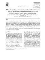
151A.A. Shklyaev et al. / Surface Science 447 (2000) 149–155
Fig. 1. (a, b) STM images of silicon islands grown at a constant current of 1.2 nA and a tip bias voltage of −10 V. In order to create
the islands (from left to right), the bias voltage was applied (a) for 1, 2, 4, 6, 9, 12 and 17 s and (b) for 8, 17, 33, 60, 120, 240, 480
and 960 s. (c, d) Height profiles along the island rows that are indicated by arrows in (a) and (b), respectively.
stage growth rate for H larger than 4 nm. The
results of the fit are shown in Fig. 2. The good
approximation to the data for island heights larger
than 4 nm by a constant rate indicates that the
late-stage growth rate was almost independent of
the island height. The early-stage growth rate was
significantly higher than the late-stage growth rate
and, as a function of the tunneling current, had a
maximum at 0.3 nA as shown in Fig. 3.
The scattering of the island height in one experi-
mental run increased with increasing tunneling
current. The increase of the scattering coincided
with the appearance of fluctuations of the tunnel-
ing current. During the growth of islands at a bias
Fig. 2. Island height as a function of the duration of bias volt-
voltage of −10 V and a tunneling current of
age. Islands were grown at a negative tip bias voltage of −10 V
and at a constant tunneling current of 1.2 nA. The solid lines
1.2 nA or larger, the fluctuations could enhance
represent the approximation of the data by a function
by themselves and could eventually reach about
H=[(a+Rt)/3]1/3 (see text) for the late growth stage and the
500 nA in amplitude. As a result of the fluctua-
insert represents the early growth stage. The scattering of the
tions, structures appeared on the silicon surface
data exceeded the accuracy of measurements of the island
height, which was within 10% (as shown for a point at 240 s).
that were like a pit or a pit near an island (Fig. 4).
The large fluctuations could flatten the apex of the
STM tip, as could be seen in SREM images of the
the equation H=[(a+Rt)/3]1/3, where a and R
tip and in the quality of STM images obtained
were used as the fitting parameters in order to
after the fluctuations. In the constant tunneling
obtain the growth rate R from the experimental
current mode of the STM operation, the fluctua-
data. We thus obtained the early-stage growth rate
tions were accompanied by mechanical vibrations
by using the range of voltage pulse durations at
which H was between 0 and 4 nm, and the late- of the STM tip in the direction normal to the
152 A.A. Shklyaev et al. / Surface Science 447 (2000) 149–155
tion of atoms of the sample followed by
re-evaporation, which transferred atoms from the
tip back to the sample. STM images showed that
these disordered structures contained silicon atoms
that were movable under the electric field of the
STM. The data also suggested that the movement
of silicon towards the island occurs through the
transfer of individual silicon atoms. Such a mecha-
nism is consistent with the fact that the amount
of silicon gathered into the island was controlled
well by the bias voltage of the pulse and its
duration [7,10]. Under the electric field E
r
, the
potential energy for surface diffusion is [11,12]
W
E
#W
0
−p · E
r
−(1/2)aE2
r
,(1)
where W
0
is the potential energy in the absence of
the electric field, p is the static dipole moment, a
is the polarizability of the atoms on the surface
(aE
r
is the induced dipole moment), and the electric
field E
r
at the sample surface decreases with
increasing radial distance r from the center of the
Fig. 3. (a) Early- and late-stage growth rates, and (b) early-
tip–sample interaction. When the mobile silicon
stage growth rate as a function of the tunneling current for
atoms on the surface have a positive electronic
tip bias voltages of (a) −10 V and (b) −8 V. The accuracy of
measurements of the early-stage growth rate at −10 V was
charge, the interaction between the electric field,
about 15–20%. The lines with arrows indicate the regions of
created by applying a negative tip bias voltage,
tunneling currents at which island growth was unstable.
and both the static and induced dipole moments
directs diffusion toward the center of the tip–
sample interaction, providing the island growth.surface. The vibration was observed by the SREM
[7] and appeared as a result of attempts to main- The kinetic data obtained in the present work
for island growth as a function of the tunnelingtain the constant tunneling current by the feedback
circuit. At large fluctuations, mechanical contact current for currents below 1 nA give us additional
insight into the mechanism of island formationbetween the STM tip and the sample could occur.
The appearance of the large pit at the place of the with the STM. At a constant tunneling current
mode of STM operation, a larger tunneling currenttip–sample interaction as shown in Fig. 4b might
be the result of the mechanical contacts. Note that corresponds to a shorter tip–sample distance s
because I~V exp(−1.1sw1/2), where I is the tunnel-atom transfer at mechanical tip–sample contacts
has been considered to explain the mound and pit ing current, V is the bias voltage, w is the effective
height of the tunnel barrier expressed in Volts, andformation on silicon surfaces in UHV when voltage
pulses were applied to a gold STM tip [5,6,9]. s is in A
˚
[13,14]. The decrease of s with increasing
I makes the electric field at the sample surfaceAt tunneling currents below 1 nA, the STM
operation was stable and the kinetic data of island stronger and therefore should increase the island
growth rate [7,10]. However, the data in Fig. 3growth were reproducible. The following experi-
mental data were obtained recently for the initial show that the early-stage growth rate increased
with increasing tunneling current only at smallstage of the tip–sample interaction which results
in island growth [7,10]. The application of elevated currents up to 0.3 nA, and the decrease of this rate
was observed at larger currents. In our case of thebias voltages to the STM tip at a constant tunnel-
ing current created an area of disordered negative tip bias polarity, atom diffusion flows
towards the center of the tip–sample interactions;Si(111)-7×7 structure by field-induced evapora-
153A.A. Shklyaev et al. / Surface Science 447 (2000) 149–155
Fig. 4. (a, b) STM images of Si(111) surfaces after tip–sample interactions at a tip bias voltage of −10 V and (a) at tunneling
currents of 0.3, 0.7, 1.3 and 3.0 nA (from top to bottom) applied for 22 s at each point, and (b) for 25 s at tunneling currents marked
in the image. (c, d ) Height profiles between the arrows marked in (a) and (b), respectively. Structures like (a) a pit near an island
and (b) a large pit are seen at the large tunneling current of 3.0 nA.
that is, in the direction opposite to the flow of growth. As an island grows, the distance between
the area around the island and the STM tipelectrons. This is similar to the effect of the electron
wind force acting at electromigration [15,16]. increases because, at a constant tunneling current,
the distance between the STM tip and the centerTherefore, the effect of the electron flow on the
direction of atom movement is opposite to the of the island is fixed. Therefore, the growth causes
the electric field to decrease at the area around theeffect of the decrease of the potential energy barri-
ers for diffusion by the electric field, which is island and, hence, the growth should cause the
growth rate to decrease according to the mecha-responsible for island growth with the STM. The
decrease of the early-stage growth rate as the nism of the early stage of growth described above.
This corresponds to the fact that the late-stagetunneling current increased ( Fig. 3) indicates that
the effect of the increasing electron flow on direc- growth rate is smaller than the early-stage growth
rate (Fig. 3a). However, at island heights betweentional diffusion dominates the effect of the increas-
ing electric field when the tunneling current 4 and 12 nm, the growth rate remains significant
and is almost independent of the island height.exceeds 0.3 nA.
The kinetic data also show the difference Moreover, the early-stage growth rate has a strong
tunneling current dependence, whereas the late-between the early stage and the late stage of island
154 A.A. Shklyaev et al. / Surface Science 447 (2000) 149–155
stage growth rate is really independent of the atom transfer with the STM. As known, adatoms
of certain chemical elements have a positive electrictunneling current. These data indicate that the
early and late growth stages have different mecha- charge [19]. First-principles calculations, per-
formed to analyze the electromigration on Si(111)nisms. Since the electric field is responsible for the
growth, the correlation between the late-stage surfaces, have shown that the effective force acting
on the diffusing atoms can be expressed throughgrowth rate and the electric field at the surface of
the STM tip apex, which does not depend on the the interaction between an electric field and a
positive charge of about 0.05 electron charge [15].island height and has a weak logarithmic depen-
dence on the tunneling current, can be taken into Therefore, in our study, positive charge can also
be expected in silicon atoms of the disorderedaccount. This correlation suggests the mechanism
in which atom transfer from the STM tip to the surface structures. A combination of this positive
charge with a corresponding negative mirrorisland due to field-induced re-evaporation of sili-
con as negative ions can contribute predominantly charge in the surface layer gives a static dipole
moment. The interaction between the static dipoleto growth at the late stage. The silicon needed for
such transfer could be accumulated on the STM moment and the non-uniform electric field of the
STM at a negative bias voltage on the tip reducestip at the initial stages of the tip–sample inter-
action. The STM images have shown that, after the potential energy barrier for diffusion towards
the center of the tip–sample interaction. In addi-the 6 s tip–sample interaction at a tip bias voltage
of −10 V, the diameter of disordered Si(111)-7×7 tion to this driving force, the interaction between
the electric field and the induced dipole momentstructure around the island was about 60 nm
[7,10]. If on average every third silicon atom is of adatoms always pushes the diffusion flow
towards the center, where the electric field isremoved from the surface bilayer in this area and
is transferred in the island, the height of the island stronger. At a given temperature and dipole
moment, the adatoms should be weakly bondedwill be 4.8 nm for cone-shaped islands with an
aspect ratio of 0.3. The estimated height is approxi- to the surface and able to diffuse under the electric
field. However, not every surface can be modifiedmately two times larger than the height of corre-
sponding real islands, suggesting that part of the with the STM at room temperature, even if ele-
vated bias voltages are applied. For example, thesilicon removed can be accumulated on the STM
tip. Note that the mechanism which includes STM-induced evaporation of SiO
2
films has been
shown to occur only at temperatures higher thanre-evaporation is consistent with the fact that the
probabilities for field-induced evaporation of nega- 450°C [20]. The well-known ability of the STM to
manipulate atoms and molecules of adsorbatestive and positive silicon ions have been found to
be almost equal [3,17]. Thus, the experimental [1,2] suggests that atoms which were adsorbed first
or deposited during the process can be involved inresults obtained in this work indicate that two
mechanisms of atom transfer contribute to the continuous atom transfer with the STM. As a
result, highly doped and compound nanostructuresisland growth: the continuous transfer of weakly
bonded silicon atoms along the sample surface is can be created. As shown here, kinetic measure-
ments of the nanostructure growth provide datagradually substituted by silicon atom transfer from
the STM tip to the island as the island height which throw light on the mechanism of nanostruc-
ture formation.increases from 0 to about 12 nm.
We have recently demonstrated that continuous
atom transfer can be used to create germanium
islands on germanium wetting layers on Si(111) 4. Conclusion
surfaces and that structures like nanowires can
also be formed when the STM tip is moved slowly The early- and late-stage rates of silicon island
growth on Si(111) surfaces with the STM werealong the surface [18]. It is important to define
the sort of conditions on the surface that are obtained as a function of tunneling current. The
dependence of the early-stage growth rate has arequired to create nanostructures by continuous
155A.A. Shklyaev et al. / Surface Science 447 (2000) 149–155
maximum at 0.3 nA, which was related to competi- References
tion between the electric-field-induced directional
diffusion and the effect of electron flow pushing
[1] J.A. Stroscio, D.M. Eigler, Science 254 (1991) 1319.
[2] Ph. Avouris, Acc. Chem. Res. 28 (1995) 95.
the diffusion in the opposite direction. At tunneling
[3] H. Uchida, D. Huang, F. Grey, M. Aono, Phys. Rev. Lett.
currents above 1 nA and at a tip bias voltage of
70 (1993) 2040.
−8 and −10 V, the growth of islands was unsta-
[4] I W. Lyo, Ph. Avouris, Science 253 (1991) 173.
ble. The late-stage growth rate was about three
[5] C.S. Chang, W.B. Su, T.T. Tsong, Phys. Rev. Lett. 72
(1994) 574.
times lower than the early-stage growth rate, and
[6 ] D. Fujita, Q. Jiang, H. Nejoh, J. Vac. Sci. Technol. B 14
was almost independent of the tunneling current
(1996) 3413.
and height of the islands. The difference between
[7] A.A. Shklyaev, M. Shibata, M. Ichikawa, Appl. Phys. Lett.
the rates was associated with different mechanisms
74 (1999) 2140.
of island growth, in which atom transfer by field-
[8] S. Maruno, H. Nakahara, S. Fujita, H. Watanabe, Y.
Kusumi, M. Ichikawa, Rev. Sci. Instrum. 68 (1997) 116.
induced diffusion on the sample surface in the
[9] T.T. Tsong, Phys. Rev. B 44 (1991) 13703.
early growth stage is gradually substituted by the
[10] A.A. Shklyaev, M. Shibata, M. Ichikawa, submitted for
transfer of silicon atoms, accumulated on the STM
publication.
tip during the initial stages of the tip–sample
[11] T.T. Tsong, G. Kellogg, Phys. Rev. B 12 (1975) 1343.
interaction, to the island by field-induced
[12] L.J. Whitman, J.A. Stroscio, R.A. Dragoset, R.J. Celotta,
Science 251 (1991) 1206.
re-evaporation in the late growth stage.
[13] G. Binning, H. Rohrer, Surf. Sci. 126 (1983) 236.
[14] J.G. Simmons, J. Appl. Phys. 34 (1963) 1793.
[15] D. Kandel, E. Kaxiras, Phys. Rev. Lett. 76 (1996) 1114.
[16 ] E.S. Fu, D J. Liu, M.D. Johnson, J.D. Weeks, E.D. Wil-
Acknowledgements
liams, Surf. Sci. 385 (1997) 259.
[17] A. Kobayashi, F. Grey, R.S. Williams, M. Aono, Science
259 (1993) 1724.
This work, partly supported by the New Energy
[18] A.A. Shklyaev, M. Shibata, M. Ichikawa, in preparation.
and Industrial Technology Development Organ-
[19] K.D. Brommer, M. Galva
´
n, A.D. Pino Jr., J.D. Joanno-
ization (NEDO), was carried out at JRCAT under
poulos, Surf. Sci. 314 (1994) 57.
an agreement between the National Institute for
[20] M. Shibata, Y. Nitta, K. Fujita, M. Ichikawa, Appl. Phys.
Lett. 73 (1998) 2179.
Advanced Interdisciplinary Research and ATP.