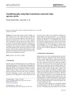
numerical study of optical nanolithography using nanoscale bow tie shaped nano apertures
Bạn đang xem bản rút gọn của tài liệu. Xem và tải ngay bản đầy đủ của tài liệu tại đây (270.71 KB, 7 trang )
Journal of Microscopy, Vol. 229, Pt 3 2008, pp. 483–489
Received 26 September 2006; accepted 16 June 2007
Numerical study of optical nanolithography using nanoscale
bow-tie–shaped nano-apertures
L. WANG & X. XU
School of Mechanical Engineering, Purdue University, West Lafayette, IN, U.S.A.
Key words. Bow-tie nano-aperture, FDTD, imaging contrast, nanolithography.
Summary
Contact lithography using bow-tie–shaped nano-apertures
was recently demonstrated to achieve nanometer scale
resolution. In this work, the detailed field distributions in
contact nanolithography are analyzed using finite difference
time domain simulations. It was found that the high imaging
contrast, which is necessary for successful lithography, is
achieved close to the mask exit plane and decays quickly
with the increase of the distance from the mask exit plane.
Simulationsare also performed for comparable regular-shaped
apertures and different shape bow-tie apertures. Design rules
are proposed to optimize the bow-tie aperture for producing
a sub-wavelength, high transmission field with high imaging
contrast.
Introduction
Low-cost nanolithography techniques, such as near-field
photolithography (Aizenberg et al., 1997; Alkaisi et al.,
1999),nano-imprintlithography(Chouet al.,1995),scanning
probe lithography (Davy & Spajer, 1996) and surface
plasmon–assisted nanolithography (Luo & Ishihara, 2004;
Srituravanich et al., 2004; Liu et al., 2005), are generating a
lot of interests recently. Standard photolithography techniques
employ a light source to define patterns in the resist, and the
minimum size of the features that can be obtained is limited to
roughly half of the wavelength of the light (Madou, 1997).
Advances in near-field optics using nanoscale light source
have achieved spatial resolution significantly better than the
diffraction limit (Rudman et al., 1992; Inouye & Kawata,
1994). However, the transmission efficiencyofcommonly used
regular shaped apertures, such as square or circular shaped
apertures is very low (Bethe, 1944). Recently, numerical (Shi
& Hesselink, 2002; Jin & Xu, 2004, 2005; Sendur et al.,
2004; Schuck et al., 2005) and experimental studies (Chen
Correspondence to: X. Xu. Tel: 1 (765) 494 5639; fax: 1 (765) 494 6539; e-mail:
et al., 2003; Matteo et al., 2004; Farahani et al., 2005; Jin &
Xu, 2006; Sundaramurthy et al., 2006; Wang et al., 2006;
Xu et al., 2006) have demonstrated high transmission and
field concentration of certain types of ridge apertures, such
as C, H and bow-tie–shaped apertures. These calculations
showed that sub-wavelength apertures have the capability
of confining light at visible wavelengths to sub-wavelength
dimensions, along with transmission efficiency much higher
than that of ordinary square- or circular-shaped apertures.
Thus, these apertures offer great potentials in applications
such as high-resolution imaging and optical data storage.
Using these apertures as an alternative to the standard IC
fabrication techniques for nanolithography is also attractive.
Recently, we have successfully demonstrated that nanoscale
bow-tie apertures can be used for contact nanolithography
to achieve nanometer scale resolution (Wang et al., 2006).
Bow-tie aperture has a longer cut-off wavelength than regular
aperture does. Visible or UV light with proper polarization
can pass through the bow-tie aperture without experiencing
much intensity decay. The transmitted light is mainly confined
underneath the tips of the bow tie, offering the optical
resolution far beyond the diffraction limit.
Understanding the characteristics of near-field optical
phenomena is an important step to improve the performance
of nanolithography (McNab & Blaikie, 2000). In this paper,
finite difference time domain (FDTD) simulations of light
transmission through bow-tie nanoapertures are conducted
to study the details of the transmitted near-field intensity
and imaging contrast for lithography. Particularly, we focus
our attention on the imaging contrast which is needed for
successful lithography but hasnot received sufficient attention
in the past studies. Our results show that, for nanolithography
applications, the bow-tie–shaped nanoaperture has much
better performance over conventional rectangular and square
apertures with the same opening area. We also show that
the imaging contrast and the transmitted near-field intensity
strongly depend on the aperture dimension, tip separation,
distance from the exit plane and the desired resolution to be
obtained.
C
2008 The Authors
Journal compilation
C
2008 The Royal Microscopical Society
484
L. WANG AND X. XU
Fig. 1. Schematics of bow-tie aperture (left) and FDTD simulated structures (right). The grey area represents metal film.
Finite difference time domain simulations
It is well known that Fourier optics is no longer adequate
for analyzing optical properties in real metals due to the
finite skin depth, film thickness and surface plasmon effect
(Goodman,1996).Rigorousvectorialanalysismustbeapplied.
The FDTD numerical method simulates the optical near filed
of light transmission through sub-wavelength apertures by
numerically solving the Maxwell’s equations. In this work, the
FDTD method is used to compute the near-field distributions of
a bow-tie aperture. The simulated geometry is shown in Fig. 1,
which consists of a 150-nm-thick aluminium film mask and
a semi-infinite photoresist layer. The bow-tie aperture has an
L × Loutline dimension witha tip separation distance of G. The
wavelength of incident light is 355 nm and the electric field is
polarized along the y direction. It is important to choose the
right metal as the material of the opaque film, as it should have
high reflection (to suppress the background light transmission
through the metal film) and small skin depth (less loss for
the light propagating through the aperture). Aluminium is
selected as the film material because of its high reflectivity and
small skin depth (reflectivity R = 0.92, skin depth = 6.5 nm)
at the exposure wavelength of 355 nm. It is also shown to
be stable in the ambient air environment during lithography
process (Wang et al., 2006).
The FDTD method was first introduced by Yee in 1966
(Yee, 1966). In FDTD algorithm, the computational region
is discretized into small cubes, called Yee cells. Each cell
has a dimension of x, y and z in Cartesian coordinates
with size less than tenth of wavelength to ensure accurate
numerical results. However, in the study of the near field of
nanostructures, the cell size should be much smaller than the
smallest dimensions of nanostructures to ensure the physical
convergence,especiallywhen the field quantities in the vicinity
of the nanostructure is of interest. In this work, 4 × 4 × 4nm
3
cells are used to model bow-tie nano-apertures. The stability
condition relating the spatial and temporal step size is used,
which is expressed as
v
max
t =
1
x
2
+
1
y
2
+
1
z
2
−1/2
, (1)
where v
max
is the maximum velocity of the wave in
the material. In addition, absorbing or perfectly matched
boundary conditions (Mur, 1981; Liao et al., 2000) must be
employed to eliminate the reflected waves on the boundaries
of the finite computational domain and to ensure accurate
results. The second-order absorbing boundary condition (Liao
et al., 2000) is used in this work. The commercial software
package XFDTD 5.3 from Remcom is used, which has been
used in many near-field calculations (Shi & Hesselink, 2002;
Jin & Xu, 2004, 2005; Sendur et al., 2004).
The modified Debye model is used to compute the complex
permittivity for aluminium, which is expressed as
ε(ω) = ε
α
+
ε
5
− ε
α
1 + jωτ
+
σ
j ωε
0
, (2)
where ε
5
represents the static permittivity, ε
∝
is the
permittivity at infinite frequency which should be no less
than 1, σ is conductivity and τ is the relaxation time. Given
the experimental refractive index data of aluminium in the
wavelength range of interest (Lide, 1996), the Debye model
parameters are found as ε
∝
= 1, ε
5
=−507.825, τ = 9.398 ×
10
−16
s and σ = 4.8 × 10
6
sm
–1
. The index of refractive used
for the photoresist is 1.6.
Results
The transmitted field intensity and imaging contrast (also
called modulation) are two important factors for lithography
patterning. Photoresist is sensitive to the total field intensity,
and sufficient imaging contrast is needed for exposing the area
that needs to be exposed for making good quality patterns
C
2008 The Authors
Journal compilation
C
2008 The Royal Microscopical Society, Journal of Microscopy, 229, 483–489
NUMERICAL STUDY OF OPTICAL NANOLITHOGRAPHY
485
Fig. 2. Intensity distribution in the x–y plane of transmitted field of bow-tie aperture (L = 160 nm, G = 24 nm) at (a) 4 nm, (b) 16 nm and (c) 40 nm
behind the exit plane
(Madou, 1997). In this report, these two factors are studied
based on the simulation results. The imaging contrast M (z, r)
is defined as:
M(z, r ) =
I
max
(z) − I (z, r)
I
max
(z) + I (z, r)
, (3)
where z is the distance from the exit plane of the aperture and r
is the radial coordinate. I
max
(z) is the peak intensity of the light
intensity in the plane with a distance z from the exit plane and
I (z,r) is the intensity where the imaging contrast needs to be
evaluated.
Figures 2 and 3 show how the imaging contrast is calculated
and used for estimating lithography performance, using the
bow-tie antenna aperture as an example. The intensity
distribution (∼E
2
) of the transmitted field in the x–y plane at
distances (z) 4 nm, 16 nm and 40 nm behind the exit plane of
the bow-tie aperture are shown. The intensity is normalized
with the incident intensity, that is, the intensity of the incident
wave is 1. The bow-tie aperture has the dimension of L = 160
nm and G = 24 nm. At a distance 4 nm from the exit plane,
the maximum field intensity (I
max
) is found near the two tips of
the bow-tie aperture. At a distance 12 nm from the exit plane,
the field intensity has decreased considerably, and the highest
intensity is at the centre (r = 0). This is true for any distance
greater than 12 nm for this bow-tie aperture.
In this work, imaging contrasts are calculated at two radius,
r = 25 nm and r = 50 nm at each distance, which is intended
to find out if the imaging contrasts are sufficient for achieving
lithography resolutions of 50 nm and 100 nm (2r). This is
illustratedinFig.3,whichshows the intensity profile across the
centre of bow-tie aperture at 32 nm from the mask exit plane.
I
max
(=0.281) is located at the centre. The intensities at r(x) =
25 nm and 50 nm are 0.180 and 0.049, respectively. From
Eq. (3), the imaging contrasts at these two locations are
calculated as 0.217 and 0.703. As shown in Fig. 3, the
intensity difference between I
max
and I (r = 50 nm) is much
larger than that between I
max
and I (r = 25 nm), which means
it is much easier to control the total dose for fabricating a
structure with a size of 100 nm than a size of 50 nm. The
minimum imaging contrast required for exposing the S1805
photoresist,whichhasbeenusedinnanolithography, isaround
0.1 (Alkaisi et al., 2000).
Once the field distribution and imaging contrast are
calculated, we can also calculate a depth of focus (DOF) for
achieving a specified resolution, which is the distance into the
photoresist where light contrast is sufficient (>0.1) to expose
the photoresist. In the following analysis, we calculate the DOF
for achieving a 50 nm resolution.
Comparisons of bow tie, square and rectangular apertures
In this session, we discuss imaging contrasts and field
intensities obtained from bow tie, square and rectangular
apertures. A bow-tie aperture with 160 nm outline dimension
(L) and 24 nm tip separation (G), a 115 nm × 115 nm
square aperture (SQ) and a 320 nm × 40 nm rectangular
aperture (REC) are computed. The dimensions of the square
and the rectangular apertures are chosen to have the same
opening area as the bow-tie aperture for the purpose of
comparison. Table 1 summarizes the calculation results of
spot size, transmission throughput, peak field intensities and
DOF of 50 nm resolution. The spot size is defined as the full
width at half magnitude (FWHM) of the intensity. The reason
to show the results at 24 nm below the exit plane is that in
lithography experiments, results are always observed with a
certain depth. From the calculation results, it can be seen that
the spot size of bow-tie aperture is smaller than those obtained
from square and rectangular apertures. The transmission
throughput is evaluated by the ratio of transmitted field
intensity integrated over the aperture area to incident field
intensity over the aperture area. The (normalized) peak field
intensity is obtained at the centre of the aperture exit plane.
It is found that the peak filed intensity of the bow-tie aperture
is 2.82 times of rectangular aperture and 25 times of square
aperture.
C
2008 The Authors
Journal compilation
C
2008 The Royal Microscopical Society, Journal of Microscopy, 229, 483–489
486
L. WANG AND X. XU
Fig. 3. Field intensity profile across the centre of the bow-tie aperture at 32 nm behind the exit plane.
The imaging contrasts for 50 nm resolution (r = 25 nm)
in x–y plane as a function of depth z from the exit plane are
shown in Fig. 4(a). It can be seen that the bow-tie aperture
has the best contrast within 50 nm from the exit plane, and
the contrast is less than that of a square aperture when the
distance is larger than 50 nm. This is because the bow-tie
aperture has the smallest spot size and the highest intensity
when it is close to the mask exit plane, and its transmitted field
diverges more quickly than rectangular and square apertures.
Given the fact that the depth of nanolithography is normally
less than 50 nm (Wang et al., 2006), the bow-tie apertures
offer the advantage for nanolithography in terms of having a
higher imaging contrast.
Figure 4(b) shows the imaging contrast for 100 nm
resolution. It is clear that all three apertures have much
better contrast than those of 50 nm resolution. This means
achieving 100 nm features is easier than achieving 50 nm
features. Similarto 50 nm resolution, is also seen that the bow-
tie aperture is better than square and rectangular apertures
for 100 nm features patterning in terms of having a higher
imaging contrast.
Comparisons of bow-tie apertures with different outline dimension
In this session, we discuss the size-dependent imaging
contrasts and intensities of bow-tie nanoapertures. Four bow-
tie apertures with different outline dimension (L): 120 nm,
160 nm, 200 nm and 300 nm are simulated. All other
dimensions are chosen to be the same: a 24-nm tip separation
and a 150-nm film thickness. Transmitted imaging contrasts
for 50 nmand 100 nm resolutionin the x–y plane asa function
of depth z from the mask exit plane are studied.
Figures 5(a) and (b) show the imaging contrast for 50 nm
and 100 nm resolution as a function of distance from the
exit plane. We found that the contrasts of all the bow-tie
apertures follow the same trends as the distance from the exit
plane is increased. However, the imaging contrasts for 50 nm
resolution are smaller than those of 100 nm resolution. This
again indicates it is more difficult to achieve 50 nm resolution
than 100 nm resolution.
A different bow-tie outline dimension can produce different
transmitted power. The normalized peak field intensity,
transmission throughput, DOF of 50 nm resolution and the
Table 1. Comparison of bow-tie and regular apertures.
Bow-tie aperture Rectangle Square
Spot size at 24 nm in the photoresist 60 nm × 60 nm 136 nm × 152 nm 88 nm × 168 nm
Transmission throughput 1.19 1.83 0.2
Peak intensity 4.00 1.42 0.16
DOF of 50 nm resolution 60 nm N/A 100 nm
C
2008 The Authors
Journal compilation
C
2008 The Royal Microscopical Society, Journal of Microscopy, 229, 483–489
NUMERICAL STUDY OF OPTICAL NANOLITHOGRAPHY
487
Fig. 4. Imaging contrast for (a) 50 nm and (b) 100 nm resolution in x–y plane as a function of depth z from the exit plane for bow tie, rectangular and
square apertures.
Fig. 5. Imaging contrast of (a) 50 nm and (b) 100 nm resolution as a function of depth z from the mask exit plane for bow-tie apertures having the same
tip separation of 24 nm. Their outline dimensions are 300 nm, 200 nm, 160 nm and 120 nm.
spot size at 24 nm from the exit plane are summarized
in Table 2. It is also found that a larger bow-tie aperture
provides a higher field intensity. This is because as the aperture
becomes larger, more light is able to be coupled into the
aperture and to be focused by bow-tie aperture due to its
light concentration function (Jin & Xu, 2005). The intensity is
therefore enhanced. However, it is noticed that if the bow-tie
aperture is larger than 160 nm, there is light leaking from the
Table 2. Comparison of different shape bow-tie apertures with same tip separation.
Bow-tie aperture outline dimensions 120 nm 160 nm 200 nm 300 nm
Spot size at 24 nm in the photoresist 60 nm × 80 nm 60 nm × 80 nm 60 nm × 88 nm 68 nm × 96 nm
Transmission throughput 1.77 1.19 0.89 0.62
Peak intensity 2.86 4.00 4.75 7.18
DOF of 50 nm resolution 56 nm 57 nm 61 nm 62 nm
C
2008 The Authors
Journal compilation
C
2008 The Royal Microscopical Society, Journal of Microscopy, 229, 483–489
488
L. WANG AND X. XU
two arms of the aperture and the transmitted spot size starts
to be elongated in y direction. Thus, carefully selecting the
aperture size is necessary to achieve both field enhancement
and concentration. The calculation results show that the
optimum size of the bow-tie outline dimension is around half
of the incident wavelength.
Comparison of bow-tie apertures with different tip separations
We also calculated transmitted near-field intensities of bow-tie
apertures with various tip separation distances. Three bow-
tie apertures are simulated with tip separation distance of
32 nm, 24 nm and 16 nm. All of them have the same outline
dimensions of 160 nm. In Fig. 6(a), the imaging contrast is
calculated for 50 nm resolution. We found that these bow-
tie apertures provide very limited intensity contrast, except
the one with the smallest tip separation. Figure 6(b) shows
the intensity contrast for 100 nm resolution. The imaging
contrasts follow the same trend, and high imaging contrasts
can be obtained for all three bow-tie apertures since the tip
separation sizes are all much smaller than 100 nm. The
bow-tie aperture with the smaller tip separation distance has
slightly better contrast. Comparing Figs 6(a) and (b), it is
seen again that achieving 50 nm resolution is much more
difficult than achieving 100 nm resolutionin terms of imaging
contrast.
Table 3. Comparison of different shape bow-tie apertures with same outline dimensions.
Tip separation 32 nm 24 nm 16 nm
Spot size at 24 nm in the photoresist 72 nm × 96 nm 60 nm × 80 nm 48 nm × 56 nm
Transmission throughput 1.15 1.19 1.26
Peak intensity 2.01 4.00 10.24
DOF of 50 nm resolution 57 nm 57 nm 57 nm
Table 3 summarized the normalized peak field intensity,
transmission throughput, DOF of 50 nm resolution and the
spotsize at24nmfrom theexitplane.Itcanbe seenthatthespot
size becomes smaller andthepeak field intensityincreaseswith
the decreasing of tip separation.Thisis because the transmitted
field is essentially induced by the dipole radiation, which has
opposite charges at the two bow-tie tips. The reduction of tip
separation increases the charge density due to the stronger
coupling between the two tips, whichincreasesthe transmitted
near-field intensity.
Fromtheabovediscussionsbasedonthe calculations results,
it can be concluded that to design nanoscale bow-tie apertures
for producing a sub-wavelength, high transmission field with
high imagingcontrast,itsoutlinedimensionandtipseparation
are two important parameters. A large aperture area can
increase the light throughput, however, its length should be
less than half the wavelength in order to avoid light leaking
from the arms. On the other hand, a small tip separation can
concentrate the light spot and increase the imaging contrast.
These two can be used as a general design rule for using bow-
tie apertures for nanolithography. On the other hand, there
are many process difficulties to overcome, such as accurate
fabrication of bow-tie apertures and maintaining an intimate
contact between the mask and the photoresist. These factors
do set a practical limit, and need to be taken into account in
actual lithography work.
Fig. 6. (a) 50 nm and (b) 100 nm resolution imaging contrast for bow-tie apertures with tip separation sizes of 32 nm, 24 nm and 16 nm.
C
2008 The Authors
Journal compilation
C
2008 The Royal Microscopical Society, Journal of Microscopy, 229, 483–489
NUMERICAL STUDY OF OPTICAL NANOLITHOGRAPHY
489
Conclusions
Imaging contrast and field intensity in nanolithography using
bow-tie apertures were investigated by computer simulations.
Results demonstrated that bow-tie apertures provide both
higher transmitted field intensity and smaller spot size than
comparable regularly shaped apertures. We also analyzed the
imaging contrast and field intensity for achieving 50 and
100 nm resolutions by varying bow-tie aperture dimension
and tip separation. It was found that achieving 50 nm
lithography resolution is much more difficult than achieving
100 nm resolution because of much smaller imaging contrast
values. Given the fact that the minimum imaging contrast
required for exposing the S1805 photoresist is 0.1, the depth
of focus for exposing 50 nm features by different shaped
nanoscale apertures with different shapes are also calculated.
The combination of a large outline dimension close to half
the wavelength and a smallest tip separation allows the
transmitted field intensity and imaging contrast of bow-tie
aperture to be optimized.
Acknowledgement
This work was performed with the support of the National
Science Foundation.
References
Aizenberg, J., Rogers, J.A., Paul, K.E. & Whitesides, G.M. (1997) Imaging
the irradiance distribution in the optical near field. Appl. Phys. Lett. 71,
3773–3775.
Alkaisi, M.M., Blaikie, R.J. & McNab, S.J. (2000) 70 nm features on 140
nm period using evanescent near field optical lithography. Microelect.
Eng. 53, 236–240.
Alkaisi, M.M., Blaikie, R.J., McNab, S.J., Cheung, R. & Cumming, D.R.S.
(1999) Sub-diffraction-limited patterning using evanescent near-field
optical lithography. Appl. Phys. Lett. 75, 3560–3562.
Bethe, H. (1944) Theory of diffraction by small holes. Phys. Rev. 66, 163–
182.
Chen, F.,Itagi, A., Bain, J.,et al. (2003) Imaging ofopticalfield confinement
in ridge waveguides fabricated on very-small-aperture laser. Appl. Phys.
Lett. 83, 3245–3247.
Chou, S.Y., Krauss, P.R. & Renstrom, P.J. (1995) Imprint of sub-25 nm vias
and trenches in polymers. Appl. Phys. Lett. 67, 3114–3116.
Davy, S. & Spajer, M. (1996) Near field optics: snapshot of the field emitted
by a nanosource using a photosensitive polymer. Appl. Phys. Lett. 69,
3306–3308.
Farahani, J.N., Pohl, D.W., Eisler, H.J. & Hecht, B. (2005) Single quantum
dot coupledtoa scanning optical antenna: atunablesuperemitter.Phys.
Rev. Lett. 95, 017402.
Goodman, J.W. (1996) Introduction to Fourier Optics, 2nd edn., Chap. 3,
McGraw-Hill, New York.
Inouye, Y. & Kawata, S. (1994) Near-field scanning optical microscope
with a metallic probe tip. Opt. Lett. 19, 159–161.
Jin, E.X. & Xu, X. (2004) Finite-difference time-domain studies on optical
transmission through planar nano-apertures in a metal Film. Jpn. J.
Appl. Phys. 43, 407–417.
Jin, E.X. & Xu, X. (2005) Obtaining super resolution light spot using
surface plasmon assisted sharp ridge nanoaperture. Appl. Phys. Lett.
86, 111106.
Jin, E.X. & Xu, X. (2006) Enhanced optical near field from a bowtie
aperture. Appl. Phys. Lett. 88, 153110.
Liao, Z.P.,Wong, H.L., Yang,B. &Yuan,Y. (1984) Atransmitting boundary
for transient wave analysis. Scientia Sinica 28, 1063–1076.
Lide, D.R. (1996) CRC Handbook of Chemistry and Physics, Vol. 12, 77th
edn., CRC Press, Boca Raton, Florida.
Liu, Z., Wei, Q. & Zhang, X. (2005) Surface plasmon interference
nanolithography. Nano. Lett. 5, 957–961.
Luo, X. & Ishihara, T. (2004) Surface plasmon resonant interference
nanolithography technique. Appl. Phys. Lett. 84, 4780–4782.
McNab, S.J. & Blaikie, R.J. (2000) Contrast in the evanescent near field of
λ/20 period gratings for photolithography. Appl. Opt. 39, 21–25.
Madou, M.J. (1997) Fundamentals of Microfabrication. CRC Press, Boca
Raton, Florida.
Matteo, J.A., Fromm, D.P., Yuen, Y., Schuck, P.J., Moerner, W.E. &
Hesselink, L. (2004) Spectral analysis of strongly enhanced visible light
transmission through single C-shaped nanoapertures. Appl. Phys. Lett.
85, 648–650.
Mur, G. (1981) Absorbing boundary conditions for the finite-difference
approximation of the time-domain electromagnetic-field equations.
IEEE Trans Electromagn Compat 23, 377–382.
Rudman, M., Lewis, A., Mallul, A., Haviv, V., Turovets, I., Shchemelinin,
A. & Nebenzahl, I. (1992) Near-field photolithography with a solid
immersion lens. J. Appl. Phys. 72, 4379.
Schuck, P.J., Fromm, D.P., Sundaramurthy, A., Kino, G.S. & Moerner, W.E.
(2005) Improving the mismatch between light and nanoscale objects
with gold bowtie nanoantennas. Phys. Rev. Lett. 94, 017402.
Sendur, K.,Challener, W.& Peng,C. (2004) Ridge waveguideas a near-field
aperture for high density data storage. J. Appl. Phys. 96, 2743–2752.
Shi, X. & Hesselink, L. (2002) Mechanisms for enhancing power
throughput from planar nano-apertures for near-field optical data
storage. Jpn. J. Appl. Phys. 41, 1632–1635.
Srituravanich,W., Fang, N., Sun, C., Luo, Q.&Zhang, X. (2004) Plasmonic
nanolithography. Nano. Lett. 4, 1085–1088.
Sundaramurthy, A., Schuck, P.J., Conley, N.R., Fromm, D.P., Kino,
G.S. & Moerner, W.E. (2006) Toward nanometer-scale optical
photolithography: utilizing the near-field of bowtie optical
nanoantennas. Nano. Lett. 6, 355–360.
Wang,L., Uppuluri, S.M., Jin, E.X. & Xu, X. (2006) Nanolithography using
high transmission nanoscale bowtie apertures. Nano. Lett. 6, 361–364.
Xu, X., Jin, E.X., Wang, L. & Uppuluri, S.M. (2006) Design, fabrication, and
characterization of nanometer-scale ridged aperture optical antenna.
Proc. SPIE 6106, 61061J.
Yee, K. (1966) Numerical solutions of initial boundary value problems
involving Maxwell’s equations in isotropic media. IEEE Trans Antennas
Propagation 14, 302–307.
C
2008 The Authors
Journal compilation
C
2008 The Royal Microscopical Society, Journal of Microscopy, 229, 483–489