obtaining super resolution light spot using surface plasmon assisted
Bạn đang xem bản rút gọn của tài liệu. Xem và tải ngay bản đầy đủ của tài liệu tại đây (277.21 KB, 3 trang )
Obtaining super resolution light spot using surface plasmon assisted
sharp ridge nanoaperture
Eric X. Jin and Xianfan Xu
a͒
School of Mechanical Engineering, Purdue University, West Lafayette, IN 47906
͑Received 15 April 2004; accepted 13 January 2005; published online 8 March 2005͒
Finite difference time domain computations is used to study surface plasmon ͑SP͒ excitation around
C- and H-shaped ridge nanoapertures made in silver film. The SP enhances optical transmission, in
addition to the transmission mechanism of the waveguide propagation mode and Fabry-Pérot-like
resonance. However, the near-field collimation of ridge aperture is found completely destroyed. On
the other hand, using a bowtie-shaped aperture with sharp ridges made in silver, the loss of near-field
collimation can be recovered. A super resolution optical spot with full width half magnitude as small
as 12 nmϫ 16 nm is achieved due to the resonant SP excitation localized at the tips of bowtie. Much
higher field enhancement is also obtained compared to the bowtie aperture made in chromium.
© 2005 American Institute of Physics. ͓DOI: 10.1063/1.1875747͔
Recently, many efforts have been made to improve trans-
mission efficiency through subwavelength apertures and ob-
tain sub-diffraction-limited light spots. A small circular or
square aperture suffers from low throughput
1
due to wave-
guide cutoff. By surrounding a circular aperture with a peri-
odic structure,
2
the emerging light can be enhanced and
beamed rather than diffracted, benefiting from the interfer-
ence of a composite diffracted evanescent wave ͓͑CDEW͒
which includes a surface plasmon component at the metal-air
interface͔.
3
However, the spatial resolution is limited by the
period of the surrounding structure which is comparable to
the wavelength.
2
Recent computational studies show that
both transmission enhancement and smaller spatial resolu-
tion can be achieved using C-,
4–8
I-,
9
or H-,
8
and bowtie
8–10
shaped ridge apertures. The collimation of transmitted light
through a C-shaped aperture has been confirmed by the near
field optical microscopy ͑NSOM͒ measurement.
11
The ridge
aperture adopts the concept of ridge waveguide in micro-
wave engineering, and has two common features: ͑1͒ open
arms which provides longer cutoff wavelength therefore al-
lows light propagating through the aperture and ͑2͒ a narrow
gap which collimates the transmitted light to a nanometer
scale region. The high cutoff wavelength enables ridge
nanoapertures to achieve nanoscale resolution using readily
available infrared, visible, and ultraviolet laser sources, al-
lowing many promising applications in NSOM imaging,
nanolithography or nanopatterning, ultrahigh density optical
data storage and thermal-assisted magnetic recording.
The transmission enhancement through a properly
designed
6
ridge aperture is associated with the TE
10
wave-
guide propagation mode,
4–8
and the Fabry-Pérot-like wave-
guide resonance
8,12,13
enhances the transmission further. In
this letter, we conduct finite difference time domain ͑FDTD͒
computations to show that surface plasmon ͑SP͒ excited
around C- and H-shaped ridge apertures in a silver film can
provide even higher transmission, but the ridge apertures
lose the near-field collimation function completely. On the
other hand, for a bowtie aperture in silver, we find that a
collimated near-field spot can be obtained in the event of
resonant SP excitation by calculating its spectrum response
at visible wavelengths. The resonant SP is a localized mode
only confined at the tips of bowtie, which contributes to both
the near-field collimation and extreme high field intensity. As
a comparison, the bowtie aperture made in a chromium film
shows a relative lower but still intense field intensity due to
the lightening rod effect instead of SP excitation.
First, we consider an H-shaped aperture in a metal film
deposited on a quartz substrate ͑dielectric constant ϭ 2.25͒
with the geometry shown in the inset of Fig. 1͑a͒. Chromium
and silver are compared to show the effect of SP. The
y-polarized illumination at 436 nm from substrate side is em-
ployed since the transmission through H-shaped aperture
with x-polarized illumination is low and no near-field colli-
mation exhibits.
8
The experimental data ͑at visible wave-
lengths͒ of complex dielectric constants of chromium
14
and
silver
15
are approximated using the Drude model.
16,17
FDTD
17
calculations are conducted to show the near-field
distributions inside and in the vicinity of the aperture by
solving the Maxwell’s equations of the differential form with
a2ϫ 2ϫ 2 spatial resolution. The thickness of metal film is
chosen to be 84 nm in order to maximize the transmission
due to the Fabry-Pérot-like resonance effect.
8,12,13
It is also
much larger than the skin depth so that the background light
transmitted through the film is suppressed.
Similar calculations on H-shaped apertures can be found
from earlier work,
8
but the emphasis here is to analyze the
electric field component and the effect of SP. In Figs. 1͑a͒
and 1͑b͒, we plot y and z components of the electric field in
the gap region of the chromium aperture on the yz plane at
x=0. We see that the field in the gap region is dominated by
the y component as expected. The y-polarized incident elec-
tric field is efficiently coupled into the aperture and well
constrained between the ridges, showing the characteristics
of the TE
10
mode. On the other hand, it is seen from Fig. 1͑b͒
that the field has a comparable z component on both the
entrance and exit planes of the aperture. Computations show
that similar field pattern of the z component can also be
found on the aperture in a perfect conductor, indicating that
this z component pattern partly results from scattering at the
aperture edges.
3
Later we will show that SP excitation con-
tributes to much higher field strength around the edges of the
aperture in a silver film. The field distribution in Fig. 1 can
a͒
Electronic mail:
APPLIED PHYSICS LETTERS 86, 111106 ͑2005͒
0003-6951/2005/86͑11͒/111106/3/$22.50 © 2005 American Institute of Physics86, 111106-1
Downloaded 18 Mar 2005 to 128.46.184.7. Redistribution subject to AIP license or copyright, see />also be understood by analyzing the aperture response to the
light. Surface current is induced on the ridges by the incident
photons at the entrance side, flows along the walls of the gap,
and reaches the exit side. When terminated by the gap, the
surface current deposits electric charges at the two ridge
edges on both entrance and exit planes. The charges oscillate
periodically in time and give the radiation field beyond the
aperture together with the TE
10
waveguide mode. Since the z
field component has similar field strength compared to that
of the waveguide mode at the exit plane and decays trans-
versely, the output near-field spot is broadened slightly.
The field patterns of y and z components in a silver
aperture are shown in Figs. 1͑c͒ and 1͑d͒, respectively. The
field strength of both the y and z components is found much
higher at the edges than those in the gap region, and the peak
field intensity at the ridge corners in silver can reach more
than 400 times of the incident field as compared to less than
36 times in chromium. The strong field strength/intensity is
associated with the SP excitation due to the facts that the
bulk plasma frequency of silver is in the visible range and
the ratio of real to imaginary parts of the dielectric constant
of silver has a large value at the excitation wavelength.
18
In
addition, the field pattern on the entrance plane ͑the quartz–
silver interface͒ in Fig. 2͑a͒ clearly shows SP excitation
around the aperture. Similar to the local excitation of SP
around a subwavelength protrusion on silver film,
18,19
here
the SP is generated by scattering from the rims of the aper-
ture ͑a topological defect on flat surface͒.
Figures 1͑c͒ and 1͑d͒ also show that the SP moves into
the aperture along the walls of the gap, in the same direction
as the TE
10
waveguide mode. When the propagating mode
and SP reach the exit plane of the aperture, the excitation of
SP occurs at the exit side around the aperture, indicated by
the strong field strength. The total transmission through the
aperture is therefore enhanced. This is quite different from
the transmission mechanism in an array of subwavelength
holes in silver, which is induced by the tunneling effect
through the subwavelength holes and interference of
CDEWs
3
or SPs
20–22
in the periodic structures. In an
H-shaped aperture, both the waveguide mode and SP excita-
tion provide the transmission enhancement. However, the
H-shaped aperture loses its near-field collimation function
completely as the transmitted light spreads around the aper-
ture instead of focusing within the gap due to the excited SP
as shown in Fig. 2͑b͒. From our calculations, this happens to
a C-shaped aperture as well ͑not shown here͒.
Also evaluated is the effect of SP on field enhancement
and near-field collimation in a bowtie aperture. The bowtie
aperture to be considered has a 90° bow angle and a narrow
gap of 4 nmϫ 4nm ͓see the inset of Fig. 3͑a͔͒ in a
60-nm-thick silver film. Fine grids of 1 nmϫ 1nmϫ 1nm
are employed in the FDTD calculations to represent an ac-
curate bowtie shape. An incident pulse containing frequency
components in the visible range is used to determine the
spectral response of the bowtie aperture by calculating the
normalized Fourier transform of a probe field at the bowtie
apex. Steady-state calculations are then conducted with a
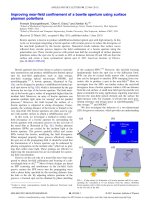
FIG. 1. Decibel scale near-field distri-
bution of electric field strength of ͑a͒ y
component and ͑b͒ z component
through the H-shaped ridge aperture in
chromium film, and ͑c͒ y component
and ͑d͒ z component in silver film on
the yz plane at x=0. The inset of ͑a͒
shows the geometry of the ridge aper-
ture. Y-polarized illumination at
436 nm is normally incident from sub-
strate side with electric field strength
of unity in air.
FIG. 2. Decibel scale near-field distribution in the vicinity of the H-shaped
ridge aperture in silver at ͑a͒ entrance plane ͑silver–quartz interface͒ and ͑b͒
exit plane ͑silver–air interface͒. The incident electric field is y polarized with
strength of unity in air.
111106-2 E. X. Jin and X. Xu Appl. Phys. Lett. 86, 111106 ͑2005͒
Downloaded 18 Mar 2005 to 128.46.184.7. Redistribution subject to AIP license or copyright, see />single plane wave illumination at 505 and 462 nm, respec-
tively ͓a peak and a valley in the spectrum response curve as
shown in the inset of Fig. 3͑b͔͒ to illustrate the bowtie aper-
ture performance at these two wavelengths, i.e., resonance
versus off-resonance.
At the 505 nm resonance, the field intensity at the
bowtie apex is found more than 15,000 times that of illumi-
nation field. A near-field optical spot ͓full width at half maxi-
mum ͑FWHM͒ of intensity͔ as small as 12 nmϫ 16 nm is
achieved at 5 nm below the aperture, and the peak intensity
is 212 times the incident intensity as shown in Fig. 3͑a͒. The
highly confined E field and the extreme high field intensity,
which is a result of the resonant SP excitation, depends on
the geometry and dielectric constants of metal and adjacent
medium.
19,23
For example, the Frohlich SP resonance for a
spherical nanoparticle occurs when
Ј
/
m
=−2 ͑where
Ј
is
the real part of dielectric constant of metal, and
m
is the
dielectric constant of adjacent medium͒ is satisfied.
23
For the
bowtie aperture in silver, SP resonance occurs at
=505 nm, where
Ј
/
m
=−8.8. This SP resonance condition
can be understood by treating each ridge of the bowtie aper-
ture as a prolate silver spheroid with axis aspect ratio of 3,
which has the Frohlich resonance at
Ј
/
m
=−8.3.
23
At this
resonance, SP is only localized at the tips of the bowtie
͑similar to the ends of the long axis of spheroid͒. In contrary,
at 462 nm off-resonance, different SP modes are excited,
which are confined at corners of bowtie aperture, and the
peak near-field intensity is reduced to 16.4 times that of il-
lumination intensity as shown in Fig. 3͑b͒.
The bowtie aperture with the same geometry as dis-
cussed previously but made in chromium is investigated as
well. Because of the large absorption and a small ratio of real
to imaginary parts of dielectric constant of chromium
͑
Ј
/
m
=−8.8 could not be satisfied͒, no sharp resonance is
observed in the spectrum response of the bowtie aperture in
chromium. The calculation shows that, with 436 nm illumi-
nation, a small optical spot with a size ͑FWHM͒ of 16 nm
ϫ 14 nm and peak intensity of about 9.24 times that of inci-
dence is obtained at 5 nm below the aperture ͓shown in Fig.
3͑c͔͒. Sine SP is very weak in chromium ͑see the results of
the H apertures͒, the field enhancement is not as high as in
silver, and is a combined result of the waveguide propagation
mode and the lightning rod or tip effect.
24
In summary, it has been explained that in addition to the
waveguide mode and Fabry-Pérot-like resonance transmis-
sion mechanisms, SP can also contribute to the transmission
enhancement in a ridge aperture in silver, but has a negative
effect on the near-field collimation for C- and H-shaped ap-
ertures. A bowtie aperture with sharp ridges would be a bet-
ter choice to achieve higher optical resolution. Benefiting
from the tip effect, a bowtie aperture in chromium has been
demonstrated to provide an optical spot with FWHM as
small as 16 nmϫ 14 nm. The bowtie aperture in silver pro-
vides comparable spot size but higher field intensity due to
the resonant excitation of SP at the sharp tips, which recovers
the loss of near-field collimation caused by the spreading of
SP around C and H apertures.
Support of this work by the National Science Foundation
is gratefully acknowledged.
1
H. A. Bethe, Phys. Rev. 66, 163 ͑1944͒.
2
H. J. Lezec, A. Degiron, E. Devaux, R. A. Linke, L. Martin-Moreno, F. J.
Garcia-vidal, and T. W. Ebbesen, Science 107, 820 ͑2002͒.
3
H. J. Lezec and T. Thio, Opt. Express 12, 3629 ͑2004͒.
4
X. Shi and L. Hesselink, Jpn. J. Appl. Phys., Part 1 41, 1632 ͑2002͒.
5
X. Shi, L. Hesselink, and R. L. Thornton, Opt. Lett. 28,1320͑2003͒.
6
X. Shi and L. Hesselink, J. Opt. Soc. Am. B 21, 1305 ͑2004͒.
7
A. V. Itagi, D. D. Stancil, J. A. Bain, and T. E. Schlesinger, Appl. Phys.
Lett. 83,4474͑2003͒.
8
E. X. Jin and X. Xu, Jpn. J. Appl. Phys., Part 1 43, 407 ͑2004͒.
9
K. Tanaka and M. Tanaka, J. Microsc. 210, 294 ͑2002͒.
10
K. Sendur and W. Challener, J. Microsc. 210, 279 ͑2002͒.
11
F. Chen, A. Itagi, J. A. Bain, D. D. Stancil, T. E. Schlesinger, L. Ste-
bounova, G. C. Walker, and B. B. Akhremitchev, Appl. Phys. Lett. 83,
3245 ͑2003͒.
12
S. Astilean, Ph. Lalanne, and M. Palamaru, Opt. Commun. 175,265
͑2000͒.
13
Y. Takakura, Phys. Rev. Lett. 86, 5601 ͑2001͒.
14
D. R. Lide, CRC Handbook of Chemistry and Physics ͑CRC Press, Boca
Raton, FL, 1996͒.
15
E. D. Palik, Handbook of Optical Constants of Solids ͑Academic, Orlando,
FL, 1985͒.
16
F Wooten, Optical Properties of Solids ͑Academic, New York, 1972͒.
17
K. Kunz and R. Luebbers, The Finite Difference Time Domain Method for
Electromagnetics ͑CRC Press, Boca Raton, FL, 1996͒.
18
H. Raether, Surface Plasmons on Smooth and Rough Surfaces and on
Gratings ͑Springer, Berlin, 1988͒.
19
H. Ditlbacher, J. R. Krenn, N. Felidj, B. Lamprecht, G. Schider, M. Sal-
erno, A. Leitner, and F. R. Aussenegg, Appl. Phys. Lett. 80,404͑2002͒.
20
T. W. Ebbesen, H. J. Lezec, H. F. Ghaemi, and T. Thio, P. A. Wolff, Nature
͑London͒ 391, 667 ͑1998͒.
21
D. E. Grupp, H. J. Lezec, T. W. Ebbesen, K. M. Pellerin, and T. Thio,
Appl. Phys. Lett. 77, 1569 ͑2000͒.
22
W. L. Barnes, A. Dereux, and T. W. Ebbesen, Nature ͑London͒ 424,824
͑2003͒.
23
C. F. Bohren and D. R. Huffman, Absorption and Scattering of Light by
Small Particles ͑Wiley, New York, 1983͒.
24
J. P. Kottmann, O. J. F. Martin, D. R. Smith, and S. Schultz, Opt. Express
6, 213 ͑2000͒.
FIG. 3. Normalized field intensity ͉͑E
t
͉
2
/͉E
0
͉
2
͒ distribution at a distance
5 nm below a bowtie aperture in ͑a͒ 60 nm silver film with 505 nm excita-
tion, ͑b͒ 60 nm silver film with 462 nm excitation; and ͑c͒ 60 nm chromium
film with 436 nm excitation. The insets show ͑a͒ the geometry of the bowtie
tips and ͑b͒ the spectrum response of the bowtie aperture in silver.
111106-3 E. X. Jin and X. Xu Appl. Phys. Lett. 86, 111106 ͑2005͒
Downloaded 18 Mar 2005 to 128.46.184.7. Redistribution subject to AIP license or copyright, see />