Điện tử cơ bản - Công thức tính phân cực tranzitor P2
Bạn đang xem bản rút gọn của tài liệu. Xem và tải ngay bản đầy đủ của tài liệu tại đây (2.87 MB, 36 trang )
CHAPTER 4 BIPOLAR JUNCTION TRANSISTORS (BJTs)
Chapter Outline
4.1 Device Structure and Physical Operation
4.2 Current-Voltage Characteristics
4.3 BJT Circuits at DC
4.4 Applying the BJT in Amplifier Design
4.5 Small-Signal Operation and Models
4.6 Basic BJT Amplifier Configurations
4.7 Biasing in BJT Amplifier Circuits
48 Discrete
Circuit BJT Amplifiers
NTUEE Electronics – L. H. Lu 4-1
4
.
8
Discrete
-
Circuit
BJT
Amplifiers
4.1 Device Structure and Physical Operation
Physical structure of bipolar junction transistor (BJT)
Both electrons and holes participate in the conduction process for bipolar devices.
BJT consists of two pn junctions constructed in a special way and connected in series, back to back.
The transistor is a three-terminal device with emitter, base and collector terminals.
From the physical structure, BJTs can be divided into two groups: npn and pnp transistors.
Modes of operation
The two junctions of BJT can be either forward or reverse-biased.
The BJT can operate in different modes depending on the junction bias.
The BJT operates in active mode for amplifier circuits.
Switching applications utilize both the cutoff and saturation modes.
NTUEE Electronics – L. H. Lu 4-2
Mode EBJ CBJ
Cutoff Reverse Reverse
Active Forward Reverse
Saturation Forward Forward
Operation of the npn transistor in the active mode
Electrons in emitter regions are injected into base due to the forward bias at EBJ.
Most of the injected electrons reach the edge of CBJ before being recombined if the base is narrow.
Electrons at the edge of CBJ will be swept into collector due to the reverse bias at CBJ.
Emitter injection efficiency (
) = i
En
/ ( i
En
+ i
Ep
)
Base transport factor (
T
) = i
Cn
/ i
En
Common-base current gain (
) = i
Cn
/ i
E
=
T
< 1
Terminal currents of BJT in active mode:
i
E
(emitter current) = i
En
(electron injection from E to B) + i
Ep
(hole injection from B to E)
i
C
(collector current) = i
Cn
(electron drift) + i
CBO
(CBJ reverse saturation current with emitter open)
i
B
(base current) = i
B1
(hole injection from B to E) + i
B2
(recombination in base region)
NTUEE Electronics – L. H. Lu 4-3
Terminal currents:
Collector current:
Base current:
Hole injection into emitter due to forward bias:
Eelectron-hole recombination in base:
Total base current:
Emitter current:
TBETBE
Vv
S
Vv
B
inBE
BnBEBnBECnC
eIe
WN
nqDA
WnqDAdxxdnqDAii
//
2
/)0(/)(
TBE
Vv
pEE
ipEE
EpEEB
e
LN
nqDA
dxxdpqDAi
/
2
1
/)(
TBE
Vv
SC
CBCE
e
Ii
iiii
/
1
TBE
Vv
nB
iE
nBEnnB
e
N
qWnA
WnqAQi
/
2
2
2
/)0(
2
1
/
C
Vv
nnBpEE
B
nB
pE
SBBB
i
e
D
W
L
W
N
N
D
D
Iiii
TBE
/
2
21
)
2
1
(
NTUEE Electronics – L. H. Lu 4-4
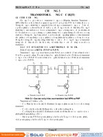
Large-signal model and current gain for BJT in active region
Common-emitter current gain:
)1/()
2
1
(
1
2
nnBpEE
B
nB
pE
B
C
D
W
L
W
N
N
D
D
i
i
Common-base current gain
i
B
i
C
i
E
1
(
+1)
1
Common-emitter
current gain
i
B
i
E
i
C
(1
)
Common-base current gain:
The structure of actual transistors
In modern process technologies, the BJT utilizes a vertical structure.
Typically,
is smaller and close to unity while
is large.
NTUEE Electronics – L. H. Lu 4-5
)1/(
Operation of the npn transistor in the saturation mode
Saturation mode: both EBJ and CBJ are forward biased
Carrier injection from both emitter and collector into base
Base minority carrier concentraiton change accordingly leading to reduced slope as v
BC
increases
Collector current drops from the value in active mode for negative v
CB
For a given v
BE
, i
C
drops sharply to zero at v
CB
around 0.5 V and v
CE
around 0.2 V.
BJT in saturation: V
CEsat
= 0.2 V
Current gain reduces from
to
forced
:
saturation
B
C
forced
i
i
NTUEE Electronics – L. H. Lu 4-6
n
p0
n
p0
exp(v
BE
/V
T
)
n
p0
exp(v
BC
/V
T
)
v
BC
increases
Ebers-Moll model
In EM model, the EBJ and CBJ are represented by two back to back diodes i
DE
and i
DC
.
The current transported from one junction to the other is presented by
F
(forward) and
R
(reverse).
EM model can be used to describe the BJT in any of its possible modes of operation.
EM model is used for more detailed dc analysis which can not be performed by the simplified models.
The diode currents:
The terminal currents:
Application of the EM model
The forward active mode:
i
i
CEB
iii
SSCRSEF
III
1
1
/
V
v
I
I
)1(
/
TBE
Vv
SEDE
eIi )1(
/
TBC
Vv
SCDC
eIi
DEFDCC
iii
DCRDEE
iii
The saturation mode:
NTUEE Electronics – L. H. Lu 4-7
i
DE
i
DC
F
i
DE
R
i
DC
i
C
i
E
i
B
F
S
Vv
F
S
E
Ie
I
i
TBE
1
1
/
1
1
/
R
S
V
v
SC
I
e
I
i
T
B
E
RF
S
Vv
F
S
B
Ie
I
i
TBE
11
/
TBC
TBE
Vv
S
Vv
SEE
eIeIi
/
/
TBC
TBE
Vv
SC
Vv
SC
eIeIi
/
/
TBC
TBE
Vv
RSC
Vv
FSEB
eIeIi
/
/
)1()1(
The cutoff mode
I
CBO
(CBJ reverse current with emitter open-circuited)
I
CBO
= (1
R
F
)I
SC
Both EBJ and CBJ are reverse-biased.
In real case, reverse current depends on v
CB
.
I
CEO
(CBJ reverse current with base open-circuited)
I
CEO
= I
CBO
/(1
F
)
F
is always smaller than unity such that I
CEO
> I
CBO
.
CBJ current flows from (C to B) so CBJ is reverse-biased.
EBJ current flows from (E to B) so
EBJ is slightly forward
-
biased.
EBJ
current
flows
from
(E
to
B)
so
EBJ
is
slightly
forward
biased.
NTUEE Electronics – L. H. Lu 4-8
+
EC
B
(2)
R
I
SC
I
SC
(1)
i
C
i
E
= 0
i
B
(3)
R
I
SC
R
F
I
SC
(4)
i
C
= I
CBO
= (1
R
F
)I
SC
(5)
i
B
= (
R
)I
SC
+ (
F
)i
DE
= 0 i
DE
= I
SC
(
R
) / (
F
) (5)
E
C
B
(2)
R
I
SC
I
SC
(1)
i
C
i
B
= 0
i
E
+
(3) i
DE
F
i
DE
(4)
i
C
= I
SC
+
F
i
DE
= I
SC
(1
R
F
)/ (1
F
) I
CEO
= I
CBO
/ (
F
) (6)
The pnp transistor
Transistor structure:
emitter and collector are p-type
base is n-type
Operation of pnp is similar to that of npn
Operation of pnp in the active mode
Collector current:
Base current:
Emitter current:
L
ildld tifBJTi ti i
TEB
Vv
SC
eIi
/
/
CB
ii
BCE
iii
L
ar
g
e-s
ig
na
l
mo
d
e
l
an
d
curren
t
g
a
i
n
f
or
BJT
i
n ac
ti
ve re
gi
on
NTUEE Electronics – L. H. Lu 4-9
Common-base current gain
i
B
i
C
i
E
1
(
+1)
1
Common-emitter
current gain
i
B
i
E
i
C
(1
)
4.2 Current-Voltage Characteristics
Circuit symbols, voltage polarities and current flow
Terminal currents are defined in the direction as current flow in active mode.
Negative values of current or voltage mean in opposite polarity (direction).
Summary of the BJT current-voltage relationships in the active mode
The values of the terminal currents for a BJT in active mode solely depend on the junction voltage of EBJ.
The ratios of the terminal currents for a BJT in active mode are constant.
The current directions for npn and pnp transistors are opposite.
NTUEE Electronics – L. H. Lu 4-10
TBE
Vv
SC
eIi
/
TBE
Vv
SC
B
e
Ii
i
/
TBE
Vv
SC
E
e
Ii
i
/
TEB
Vv
SC
eIi
/
TEB
Vv
SC
B
e
Ii
i
/
TEB
Vv
SC
E
e
Ii
i
/
BCE
iii
1
1
pnp transistornpn transistor
Current-voltage characteristics of BJT
The i
C
-v
CB
characteristics The i
C
-v
CE
characteristics
The Early effect
As CBJ reverse bias increases, the effective base width W
eff
reduces due to the increasing CBJ depletion.
For a constant junction voltage v
BE
:
The slope of n
B
(x) increases i
C
increases
Charge storage Q
n
reduces i
B
decreases
Current gain
and
increases
Early voltage (V
A
) is used for the linear approximation of Early Effect.
Linear dependence of i
C
on v
CE
:
Exhibit finite output resistance:
NTUEE Electronics – L. H. Lu 4-11
n
B
(0)
n
B0
0 W
X
W
Y
W
Z
V
Y
V
Z
V
X
)/1(
/
ACE
Vv
SC
VveIi
TBE
C
A
constantv
CE
C
o
I
V
v
i
r
BE
1
Common-base output characteristics
breakdownEarly effect
i
C
versus v
CB
plot with various i
E
as parameter is known as common-base output characteristics
The slope indicates that i
C
depends to a small extent on v
CB
Early effect
i
C
increases rapidly at high v
CB
breakdown
BCJ is slightly forward-biased for 0.4V < v
CB
< 0
No significant change is observed in i
C
The BJT still exhibits I-V characteristics as in the active mode
BCJ turns on strongly and the i
C
starts to decrease for v
BC
< 0.4V
I-V characteristics in the saturation mode and v
CEsat
is considered a constant ( 0.2 V)
Current gain (
): large-signal
i
C
/i
E
and small-signal (incremental)
i
C
/i
E
NTUEE Electronics – L. H. Lu 4-12
Common-emitter output characteristics (I)
i
C
versus v
CE
plot with various v
BE
as parameter.
Common-emitter current gain is defined as
= i
C
/ i
B
The BCJ turns on with a positive v
BC
at low v
CE
BJT operates in saturation mode
The i
C
curve has a finite slope due to Early effect
The characteristics lines meet at v
CE
= V
A
V
A
is called the Early Voltage (~ 50 to 100 V)
Common-emitter output characteristics (II)
Plot of i
C
versus v
CE
with various i
B
as parameter
BJT in active region acts as a current source
with high (but finite) output resistance
The cutoff mode in common-emitter configuration
is defined as i
B
= 0
Current gain: large-signal
dc
i
C
/i
B
and
ac
i
C
/i
B
NTUEE Electronics – L. H. Lu 4-13
breakdownEarly effect
Saturation of common-emitter configuration
In saturation region, it behaves as a closed switch with a small resistance R
CEsat
The saturation IV curve can be approximated by a straight line intersecting the v
CE
axis at V
CEoff
The saturation voltage V
CEsat
V
CEoff
+ I
Csat
R
CEsat
V
CEsat
is normally treated as a constant of 0.2 V for simplicity regardless the value of i
C
Incremental
in saturation is lower than that in active region:
forced
I
Csat
/ I
B
<
Overdrive factor
/
forced
NTUEE Electronics – L. H. Lu 4-14
Transistor breakdown
Transistor breakdown mechanism:
Avalanche breakdown: avalanche multiplication mechanism takes place at CBJ or EBJ
Base punch-through effect: the base width reduces to zero at high CBJ reverse bias
In CB configuration, BV
CBO
is defined at i
E
= 0.
The breakdown voltage is smaller than BV
CBO
for i
E
> 0.
In CE configuration, BV
CEO
is defined at i
B
=0.
The breakdown voltage is smaller than BV
CEO
for i
B
> 0.
Typically, BV
CEO
is about half of BV
CBO
.
Breakdown of the BCJ is not destructive as long as the power dissipation is kept within safe limits
Breakdown
of
the
BCJ
is
not
destructive
as
long
as
the
power
dissipation
is
kept
within
safe
limits
.
Breakdown of the EBJ is destructive because it will cause permanent degradation of
NTUEE Electronics – L. H. Lu 4-15
4.3 BJT Circuits at DC
BJT operation modes
The BJT operation mode depends on the voltages at EBJ and BCJ
The I-V characteristics are strongly nonlinear
Simplified models and classifications are needed to speed up the hand-calculation analysis
Mode EBJ CBJ
Active Forward Reverse
Cutoff Reverse Reverse
Saturation Forward Forward
Inverse Reverse Forward
v
BE
v
BC
Active Mode
v
BE
0, v
BC
0
Saturation Mode
v
BE
0, v
BC
0
Inverse Mode
v
BE
0, v
BC
0
Cutoff Mode
v
BE
0, v
BC
0
npn transistor
v
EB
v
CB
Active Mode
v
EB
0, v
CB
0
Saturation Mode
v
EB
0, v
CB
0
Inverse Mode
v
EB
0, v
CB
0
Cutoff Mode
v
EB
0, v
CB
0
pnp transistor
Simplified models and classifications for the operation of the npn BJT
Cut-off mode:
i
E
= i
C
= i
B
= 0
v
BE
< 0.5 V and v
BC
< 0.4 V
Active mode:
v
BE
= 0.7 V and i
B
: i
C
: i
E
= 1:
: (1+
)
v
CE
> 0.3 V
Saturation mode:
v
BE
= 0.7 V and v
CE
= 0.2 V
i
C
/i
B
=
forced
<
NTUEE Electronics – L. H. Lu 4-16
Equivalent circuit models
NTUEE Electronics – L. H. Lu 4-17
DC analysis of BJT circuits
Step 1: assume the operation mode
Step 2: use the conditions or model for circuit analysis
Step 3: verify the solution
Step 4: repeat the above steps with another assumption if necessary
Example 4.4
Example 4.5
NTUEE Electronics – L. H. Lu 4-18
Example 4.9
Example 4 11
Example
4
.
11
NTUEE Electronics – L. H. Lu 4-19
4.4 Applying the BJT in Amplifier Design
BJT voltage amplifier
A BJT circuit with a collector resistor R
C
can be used as a simple voltage amplifier
Base terminal is used the amplifier input and the collector is considered the amplifier output
The voltage transfer characteristic (VTC) is obtained by solving the circuit from low to high v
BE
Cutoff mode:
0 V v
BE
< 0.5 V and i
C
= 0
v
O
= v
CE
= V
CC
Active mode:
v
BE
> 0.5 V and i
C
= I
S
exp(v
BE
/V
T
)
v
O
=
V
CC
i
C
R
C
=
V
CC
R
C
I
S
exp
(
v
BE
/
V
T
)
v
O
V
CC
i
C
R
C
V
CC
R
C
I
S
exp
(
v
BE
/
V
T
)
Saturation:
v
BE
further increases
v
CE
= v
CEsat
= 0.2 V
v
O
= 0.2 V
NTUEE Electronics – L. H. Lu 4-20
Biasing the circuit to obtain linear amplification
The slope in the VTC indicates voltage gain
BJT in active mode can be used as voltage amplification
Point Q is known as bias point or dc operating point
I
C
= I
S
exp(V
BE
/V
T
)
The signal to be amplified is superimposed on V
BE
v
BE
(t) = V
BE
+ v
be
(t)
The time-varying part in v
CE
(t) is the amplified signal
The circuit can be used as a linear amplifier if:
A proper bias point is chosen for gain
A
proper
bias
point
is
chosen
for
gain
The input signal is small in amplitude
The small-signal voltage gain
The amplifier gain is the slope at Q:
Voltage gain depends on I
C
and R
C
Maximum voltage gain of the amplifier
NTUEE Electronics – L. H. Lu 4-21
C
T
C
Vv
BE
CE
v
R
V
I
dv
dv
A
BEBE
||
maxv
T
CC
T
CECC
C
T
C
v
A
V
V
V
VV
R
V
I
A
Determining the VTC by graphical analysis
Provides more insight into the circuit operation
Load line: the straight line represents in effect the load
i
C
= (V
CC
V
CE
)/R
C
The operating point is the intersection point
Locating the bias point Q
The bias point (intersection) is determined by properly choosing the load line
The output voltage is bounded by V
CC
(upper bound) and V
CEsat
(lower bound)
The load line determines the voltage gain
The bias point determines the headroom or maximum upper/lower voltage swing of the amplifier
The
bias
point
determines
the
headroom
or
maximum
upper/lower
voltage
swing
of
the
amplifier
NTUEE Electronics – L. H. Lu 4-22
4.5 Small-Signal Operation and Models
The collector current and the transconductance
The total quantities (ac + dc) of the collector current:
Small-signal approximation: v
be
<< V
T
The transconductance indicates the incremental change of i
C
versus change of v
BE
Th
tdt
idt i dbitd ll t t
I
TbeTbeTBETBE
Vv
C
Vv
VV
S
Vv
SC
beBEBE
eIeeIeIi
vVv
//
//
)(
be
T
C
C
T
be
CcCC
v
V
I
I
V
v
IiIi
1
T
C
Ii
BE
C
m
V
I
v
i
g
CC
Th
e
t
ranscon
d
uc
t
ance
g
m
i
s
d
e
t
erm
i
ne
d
b
y
it
s
d
c co
ll
ec
t
or curren
t
I
C
General, BJTs have relatively high transconductance compared with FETs at the same current level.
The base current and the input resistance at the base
The total quantities (ac + dc) of the base current:
Small-signal approximation:
Resistance r
is the small-signal input resistance between base and emitter (looking into the base)
NTUEE Electronics – L. H. Lu 4-23
TbeTbe
TBETBE
Vv
B
VvVV
S
Vv
SC
B
eIee
I
e
II
i
////
be
T
B
B
T
be
BbBB
v
V
I
I
V
v
IiIi
1
B
T
mb
be
I
V
gi
v
r
The emitter current and the input resistance at the emitter
The total quantities (ac + dc) of the emitter current:
Small-signal approximation:
Relation between r
and r
e
:
cCC
eEE
iII
iIi
mmE
T
e
be
e
ggI
V
i
v
r
1
be
T
E
be
T
C
be
mc
e
v
V
I
v
V
I
v
gi
i
e
r
Output resistance accounting for Early effect
Use the collector current equation with linear v
CE
dependence:
The output resistance r
o
is included to represent Early Effect of the BJT
The resulting r
o
is typically a large resistance and can be neglected to simplify the analysis
NTUEE Electronics – L. H. Lu 4-24
e
rr )1(
m
m
e
g
r
g
A
CE
Vv
SC
V
v
eIi
TBE
1
/
C
A
constantv
CE
C
o
I
V
v
i
r
BE
1
BJT small-signal models
Two models are exchangeable and does not affect the analysis result
The hybrid- model
Typically used as the emitter is grounded
Neglect r
o
The T model
Typically used as the emitter is not grounded
NTUEE Electronics – L. H. Lu 4-25
Neglect r
o