Lasers Applications in Science and Industry Part 1 ppt
Bạn đang xem bản rút gọn của tài liệu. Xem và tải ngay bản đầy đủ của tài liệu tại đây (2.09 MB, 20 trang )
LASERS – APPLICATIONS IN
SCIENCE AND INDUSTRY
Edited by Krzysztof Jakubczak
Lasers – Applications in Science and Industry
Edited by Krzysztof Jakubczak
Published by InTech
Janeza Trdine 9, 51000 Rijeka, Croatia
Copyright © 2011 InTech
All chapters are Open Access distributed under the Creative Commons Attribution 3.0
license, which allows users to download, copy and build upon published articles even for
commercial purposes, as long as the author and publisher are properly credited, which
ensures maximum dissemination and a wider impact of our publications. After this work
has been published by InTech, authors have the right to republish it, in whole or part, in
any publication of which they are the author, and to make other personal use of the
work. Any republication, referencing or personal use of the work must explicitly identify
the original source.
As for readers, this license allows users to download, copy and build upon published
chapters even for commercial purposes, as long as the author and publisher are properly
credited, which ensures maximum dissemination and a wider impact of our publications.
Notice
Statements and opinions expressed in the chapters are these of the individual contributors
and not necessarily those of the editors or publisher. No responsibility is accepted for the
accuracy of information contained in the published chapters. The publisher assumes no
responsibility for any damage or injury to persons or property arising out of the use of any
materials, instructions, methods or ideas contained in the book.
Publishing Process Manager Petra Nenadic
Technical Editor Teodora Smiljanic
Cover Designer InTech Design Team
Image Copyright Matej Pavlansky, 2010. Used under license from Shutterstock.com
First published December, 2011
Printed in Croatia
A free online edition of this book is available at www.intechopen.com
Additional hard copies can be obtained from
Lasers – Applications in Science and Industry, Edited by Krzysztof Jakubczak
p. cm.
ISBN 978-953-307-755-0
free online editions of InTech
Books and Journals can be found at
www.intechopen.com
Contents
Preface IX
Part 1 Thin Films and Nanostructures 1
Chapter 1 Nanoparticles and Nanostructures Fabricated
Using Femtosecond Laser Pulses 3
Chih Wei Luo
Chapter 2 Production of Optical Coatings Resistant to
Damage by Petawatt Class Laser Pulses 23
John Bellum, Patrick Rambo, Jens Schwarz, Ian Smith,
Mark Kimmel, Damon Kletecka and Briggs Atherton
Chapter 3 Effect of Pulse Laser Duration and Shape on
PLD Thin Films Morphology and Structure 53
Carmen Ristoscu and Ion N. Mihailescu
Chapter 4 Laser Pulse Patterning on Phase Change Thin Films 75
Jingsong Wei and Mufei Xiao
Chapter 5 Laser Patterning Utilizing Masked Buffer Layer 93
Ori Stein and Micha Asscher
Part 2 Laser-Matter Interaction 107
Chapter 6 Interaction Between Pulsed Laser and Materials 109
Jinghua Han and Yaguo Li
Chapter 7 Pulse Laser Ablation by Reflection of Laser Pulse at
Interface of Transparent Materials 131
Kunihito Nagayama, Yuji Utsunomiya,
Takashi Kajiwara and Takashi Nishiyama
Chapter 8 Pulsed-Laser Ablation of Au Foil in Primary Alcohols
Influenced by Direct Current 151
Karolína Šišková
VI Contents
Chapter 9 Application of Pulsed Laser Fabrication in
Localized Corrosion Research 173
M. Sakairi, K. Yanada, T. Kikuchi, Y. Oya and Y. Kojima
Part 3 Biological Applications 191
Chapter 10 Laser Pulse Application in IVF 193
Carrie Bedient, Pallavi Khanna and Nina Desai
Chapter 11 Dynamic Analysis of Laser Ablation of Biological Tissue by
Optical Coherence Tomography 215
Masato Ohmi and Masamitsu Haruna
Chapter 12 Polarization Detection of Molecular Alignment Using
Femtosecond Laser Pulse 229
Nan Xu, Jianwei Li, Jian Li, Zhixin Zhang and Qiming Fan
Part 4 Other Applications 247
Chapter 13 Deconvolution of Long-Pulse Lidar Profiles 249
Ljuan L. Gurdev, Tanja N. Dreischuh and Dimitar V. Stoyanov
Preface
Recent advents in laser technology and discoveries in laser physics have enabled their
very new and exciting applications. Some of them cover production of new materials:
nano-particles, periodic structures in nano-scale, and thin films. Others allowed better
understanding of laser-matter interaction when sample is subjected to intense laser
pulses of various time duration, shape in space and time domains as well as different
spectral components contained in a pulse. This allowed control of molecules behavior
in electromagnetic field, control of chemical reactions or even direct examination of
intra-atomic processes with femtosecond or even attosecond resolution.
Lasers are also a perfect tool for medicine: since there is no contact of a tool with the
tissue they are naturally aseptic; there is now tool wear and potential bio-
contamination is minimized leading to minimum after-treatment trauma. Their
development allowed appearing of new metrology: optical coherence tomography
(OCT) which is now a routinely used device in vast majority of the hospitals. Finally,
they found their use is very sophisticated applications like in-vitro fertilization or
varicose veins treatment with a fiber laser with extremely short required patient stay
in the hospital.
Dr. Krzysztof Jakubczak
Croma Polska Sp. z o.o.
Warsaw
Poland
Part 1
Thin Films and Nanostructures
1
Nanoparticles and Nanostructures
Fabricated Using Femtosecond
Laser Pulses
Chih Wei Luo
Department of Electrophysics, National Chiao
Tung University, Taiwan
Republic of China
1. Introduction
Recently, the processing of materials by femtosecond (fs) laser pulses has attracted a great
deal of attention, because fs pulse energy can be precisely and rapidly transferred to the
materials without thermal effects (Stuart et al., 1995). In particularly, periodic
microstructures can be produced in almost any materials using fs pulses directly and
without the need for masks or chemical photoresists to relieve the environmental concerns.
For instance, nanoripples (Hsu et al., 2007; Luo et al., 2008; Sakabe et al., 2009; Jia et al., 2010;
Yang et al., 2010; Bonse & Krüger, 2010; Okamuro et al., 2010; Huang et al., 2009),
nanoparticles (Jia et al., 2006; Luo et al., 2008; Teng et al., 2010), nanocones (Nayak et al.,
2008), and nanospikes (Zhao et al., 2007b) have been induced in various materials using
single-beam fs laser pulses in air. In addition, fs laser ablation for metals and
semiconductors in a vacuum environment (Amoruso et al., 2004; Liu et al., 2007a) and in
liquid (Tsuji et al., 2003) have also been extensively investigated. These results are a strong
indicator of the application potential of fs laser pulses in science and industry.
In this chapter, we demonstrate the generation of nanoparticles and nanostructures
(including ripples and dots) using fs laser pulses. Initially, we selected the II-VI
semiconductor ZnSe to demonstrate the fabrication of nanoparticles. Following the
irradiation of fs laser pulses at a wavelength of 800 nm and pulse duration of 80 fs, many
hexagonal-phase ZnSe nanoparticles formed on the surface of an undoped (100) cubic ZnSe
single-crystal wafer. The interesting phase transition from the cubic structure of ZnSe single-
crystal wafer to the hexagonal structure of ZnSe nanoparticles may have been caused by the
ultra-high ablation pressure at the local area due to the sudden injection of high-energy
leading to solid-solid transition. This chapter discusses the details of the mechanisms
underlying this process.
In the second part of this chapter, we introduce controllable nanoripple and nanodot
structures to high-T
c
superconducting YBa
2
Cu
3
O
7
(YBCO) thin films. We also introduce the
surface morphology of YBCO thin films under single-beam and dual-beam fs laser
irradiation. The generation of periodic ripple and dot structures is determined by the
application of laser fluence, the number of pulses, polarization and the incident angles of the
laser beam. The period and orientation of ripples and even the size and density of dots can
be controlled by these parameters.
Lasers – Applications in Science and Industry
4
2. Fabrication of hexagonal-phase ZnSe nanoparticles
Zinc selenide (ZnSe) has been studied extensively since the 1970s for implementation in II-
VI semiconductors, due to its promising opto-electrical and electrical properties of direct
wide band gap 2.7 eV at 300 K (Tawara et al., 1999; Dinger et al., 2000; Xiang et al., 2003).
Over the last decade, the development of nanotechnologies has had a tremendous impact on
industry and basic scientific research. The nanostructures of ZnSe, in particular, have
attracted considerable attention recently (Tawara et al., 1999; Sarigiannis et al., 2002).
Generally, crystalline ZnSe exhibits two structural phases, cubic and hexagonal. In ambient
environments, the cubic phase is most often studies because the hexagonal structure is
thermodynamically unstable (Sarigiannis et al., 2002; Che et al., 2004). In this section, we
demonstrate the fabrication of hexagonal-phase ZnSe nanoparticles using femtosecond laser
pulses and characterize their properties.
2.1 Experimental setup and procedure
In this study, the laser source plays an important role causing materials to undergo various
changes. To reach the nonlinear region, a light source with high pulse energy is required.
The seed pulses at 800 nm were produced using a mode-locked Ti:sapphire laser (Coherent-
Micra10) pumped by a diode pump solid state laser (Coherent-Verdi). After being stretched
to ~200 ps, these pulses were synchronously injected into a Ti:sapphire regenerative
amplifier (Coherent-Legend) pumped by a 5-kHz Nd:YLF laser and the amplified pulses
(pulse energy ~0.4 mJ) were recompressed toτ
p
~ 80 fs at sample surface.
Figure 1 shows the experimental setup used for the fabrication of ZnSe nanoparticles. A plano-
convex fused silica cylindrical lens with the focal length of 100 mm was used to focus the
femtosecond laser pulses into a line spot (2270 μm×54 μm). The (100) cubic ZnSe single-crystal
wafers were mounted on a motorized X-Y-Z translation stage in air and scanned using the
focused laser spot at the scanning speed of 100 µm/s as shown in Fig. 1. The pulse energy was
varied using metallic neutral density filters with OD0.1-OD2 (Thorlabs ND series).
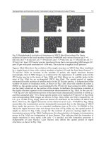
Following femtosecond laser irradiation, a white-yellow powder [as shown in the inset of
Fig. 2(b)], i.e. ZnSe nanoparticles, was observed on the surface of a ZnSe single-crystal
wafer. Depending on the experimental objectives, these ZnSe nanoparticles could be
dissolved in ethanol with ultrasonic waves or picked up with Scotch tape. After removing
Fig. 1. Experimental setup for the fabrication of ZnSe nanoparticles.
Nanoparticles and Nanostructures Fabricated Using Femtosecond Laser Pulses
5
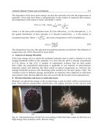
the ZnSe nanoparticles from the surface of a ZnSe single-crystal wafer, many sub-
wavelength ripples were observed on the surface, as shown in Fig. 2(b). These ripples
appeared perpendicular to the scanning direction of the laser beam and the polarization of
laser pulses, which are presented by the dashed and solid arrows, respectively, in Fig. 2(b).
Fig. 2. SEM images of ZnSe single-crystal wafers; (a) before; and (b) after femtosecond laser
pulse irradiations. Inset: OM images of ZnSe single-crystal wafer; (a) before; and (b) after
femtosecond laser pulse irradiations. The dashed arrow indicates the scanning direction of a
laser beam. The solid arrow indicates the polarization of laser pulses.
2.2 Characteristics of ZnSe nanoparticles
Figure 3(a) shows X-ray diffraction patterns of ZnSe nanoparticles fabricated at various
fluences, which can be indexed by the hexagonal structure according to the JCPDS card
no.80-0008 for ZnSe (a = b = 3.974 Å, c = 6.506 Å). It can be clearly seen that the cubic phase
of the ZnSe single-crystal wafers has been transferred to the hexagonal phase in the ZnSe
nanoparticles. Because hexagonal ZnSe is a metastable phase under ambient conditions, it
can only be fabricated under the very strict growth conditions (Jiang et al., 2004; Liu et al.,
2007b). However, hexagonal ZnSe nanoparticles can be easily and reliably achieved using
femtosecond laser ablation as demonstrated in this study. Additionally, Figure 3(b) shows
the room-temperature Raman scattering spectra of the ZnSe wafer, before and after the laser
irradiation, and fabricated nanoparticles. The Raman peak at 252 cm
-1
can be assigned to the
longitudinal optical (LO) phonon mode of the cubic structure observed both in the ZnSe
wafer before and after laser processing. For ZnSe nanoparticles, a strong peak appears at 234
cm
-1
which is the so-called surface phonon mode (Shan et al., 2006). Typically, this surface
phonon mode is a characteristic feature of nanostructures due to their large surface to
volume ratio. Besides, no LO phonon mode of cubic structure is observed in ZnSe
nanoparticles indicating that the crystal structure of ZnSe nanoparticles is pure hexagonal
phase which is in accord with the X-ray diffraction patterns shown in Fig. 3(a).
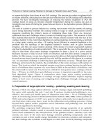
Figure 4(a) shows a typical TEM image of ZnSe nanoparticles with the smooth spherical
shape. A high-resolution TEM image at the atomic scale for one ZnSe nanoparticle is
presented in the inset of Fig. 4(b). Furthermore, the six-fold electron diffraction pattern can
be clearly observed in Fig. 4(b). Through the analysis of distance and angles between the
nearest diffraction points and the center (biggest) point, the crystal structure of ZnSe
nanoparticles was identified as a hexagonal and the orientation of each diffraction point is
Lasers – Applications in Science and Industry
6
marked in Fig. 4(b), which consists with the results of XRD in Fig. 3(a). The energy
dispersive spectroscopy (EDS) spectrum in the inset of Fig. 4(a) illustrates the composition
of these ZnSe nanoparticles, comprising only two elements of Zn and Se. This reveals that
the high purity of hexagonal ZnSe nanoparticles can be reliably and simply fabricated using
femtosecond laser pulses.
Fig. 3. (a) X-ray diffraction patterns of ZnSe wafer and ZnSe nanoparticles fabricated at
various laser fluences. H: Hexagonal. C: Cubic. (b) Raman spectra of ZnSe wafer and ZnSe
nanoparticles fabricated at the fluence of 220 mJ/cm
2
. The 632.8 nm line of laser with 0.33
mW was used as the excitation light.
Fig. 4. (a) TEM images of ZnSe nanoparticles fabricated by the fluence of 220 mJ/cm
2
. (b)
TEM diffraction patterns of ZnSe nanoparticles in (a). Insets: (a) The EDS spectrum shows
the composition of ZnSe nanoparticles; (b) High-resolution TEM image at the atomic scale.
Nanoparticles and Nanostructures Fabricated Using Femtosecond Laser Pulses
7
Fig. 5. Size distribution of ZnSe nanoparticles at various laser fluences corresponding to the TEM
images in Fig. 4(a) with an area of 3.2 μm × 2.6 μm. The solid lines are the log-normal fitting.
The size distribution of ZnSe nanoparticles fabricated at various fluences was analyzed in
Fig. 5. By the fitting of the log-normal function, we determined that the average diameter of
ZnSe nanoparticles was approximately 16 nm in the case of 135 mJ/cm
2
. With an increase in
the laser fluence to 198 mJ/cm
2
and 220 mJ/cm
2
, the average size of the ZnSe nanoparticles
increased to 20 nm and 22 nm, respectively. This indicates that the size of ZnSe
nanoparticles can be controlled by laser fluence. Furthermore, the generation rate of ZnSe
nanoparticles using fs laser pulses is approximately 3.63×10
10
s
-1
(or 7.26×10
6
per pulse) with
a fluence of 135 mJ/cm
2
. For the higher fluence of 220 mJ/cm
2
, the generation rate of ZnSe
nanoparticles increased by one order of magnitude to 3.63×10
11
s
-1
(or 7.26×10
7
per pulse).
2.3 Mechanism underlying the formation of hexagonal ZnSe nanoparticles
During femtosecond laser irradiation, a large amount of energy is transferred to the
specimens thereby inducing dense plasma on the surface of the sample. However, the
duration of energy transfer (~80 fs) is too short for the lattice and the energy is only
absorbed by the electrons within the extremely short interaction time. The ablated plume is
confined within the laser focused position of the laser by the surrounding air. Thus, the
rapidly cooling leads to the formation of nanoparticles on the surface of samples within the
ablated plume to avoid a reaction with the air. That is the reason for the lack of impurities in
the ZnSe nanoparticles fabricated by fs laser pulses in a study.
According to the early research, ZnSe transforms from a cubic structure to the hexagonal
structure when the temperature is above the transition temperature (T
tr
) of 1698 K (Rudolph
et al., 1995). When ZnSe crystals are irradiated by the femtosecond laser pulses, the
Lasers – Applications in Science and Industry
8
temperature of the ZnSe crystals increases. In the case of pulse lasers, an increases in the
transient temperature ΔT in materials can be estimated according to the relationship of ΔT =
W/(C×V), where W is the pulse energy, C is the heat capacity, and V is the illuminated
volume. For ZnSe at 300 K, C is 1.89×10
6
J/m
3
K (Martienssen & Warlimont, 2005), V is
2.29×10
-13
m
3
[absorption depth ~1.87 μm estimated from the nonlinear absorption
coefficient β (Tseng et al., 1996)], and W is on the order of 0.243 mJ (which is assumed to be
totally absorbed by ZnSe). Thus, the ΔT is approximately 560 K, which is far below the
structural transition temperature of 1698 K. Therefore, a structural transition could not be
induced by the increase in temperature. To identify the mechanism underlying the phase
transition of ZnSe from cubic to hexagonal, we further analyzed the influence of “ablation
pressure” (Batani et al., 2003), which has been studied from various perspectives over the
past few decades (Key et al., 1980; Groot et al., 1992). When solids are irradiated by laser
pulses, high-density plasma is formed on the surface of the samples. The compressed
plasma in laser driven implosions has been characterized as the ablating or exploding
pusher according to the surface ablation pressure and bulk pressure due to the preheating
through electrons.
In 2003, Batani et al. (Batani et al., 2003) derived the shock pressure with the laser and target
parameters expressed as
71
31
16 8
44
14
(Mbar) 11.6( ) ( ) ( )
23.5
10
IAZt
P
Z
(1)
where I is the laser intensity on target with the unit of W/cm
2
, λ is the laser wavelength in
µm, A and Z are, respectively, the mass number and the atomic number of the target, and t
is the time in ns. Figure 6 shows the effective pressure in the irradiated region with the laser
Fig. 6. Simulated ablation pressure as a function of the laser peak power density according
to the Eq. (1). The shadow area indicates the range of laser peak power density in this study
and corresponding ablation pressure. The dashed line represents the pressure of cubic-
hexagonal phase transition, was obtained from ref. (Greene et al., 1995).
Nanoparticles and Nanostructures Fabricated Using Femtosecond Laser Pulses
9
peak power density of the laser of 0 ~ 3.0×10
12
W/cm
2
. In this study, the maximum pressure
induced by the laser reached approximately 1.5 Mbar. According to the studies of Greene et
al. in II-VI compounds (Greene et al., 1995), the solid-solid transition point, i.e. the cubic-
hexagonal phase transition, of ZnSe is approximately 0.55 Mbar. In our experiments, the
ablation pressure induced by the femtosecond laser pulses on the ZnSe single crystals was
in the range of 1.0 Mbar to 1.5 Mbar as shown in the shadow area of Fig. 6. This exceeds the
solid-solid transition pressure 0.55 Mbar (the dashed line in Fig. 6). Therefore, the
hexagonal-phase ZnSe nanoparticles transferred from the cubic phase may be caused by
high ablation pressure resulting from the femtosecond laser pulses, and the accompanied
increase in surface to volume ratio in the nanoparticles.
3. Generation of nanoripples and nanodots on YBCO
Issues related to energy have gradually gained in value and attracted attention around
world and, the high-T
c
superconducting YBa
2
Cu
3
O
7
(YBCO) has potential as an alternative
material for green energy applications, e.g. electric power cables, transformers, motors,
electric power generators, magnetic levitation systems, due to its high critical current of 77
K. For commercialization, critical current is the key parameter, and fs laser pulses may
provide a new avenue to enhance the critical current of YBCO thin films. In this section, we
demonstrate the formation of laser-induced subwavelength periodic surface structures
(LIPSS), such as ripples and dots, on YBCO thin films using femtosecond laser and
characterize their properties.
3.1 Preparation of YBCO thin films
The YBCO thin films used in this study were prepared by pulse laser deposition (PLD) with a
KrF excimer laser operating at a repetition rate of 3-8 Hz with an energy density of 2-4 J/cm
2
as shown in the inset of Fig. 7(a). The oxygen partial pressure during deposition was
maintained at 0.25 Torr, and the substrate temperature was maintained at 780-790
o
C. After
completion of the deposition process, the film was cooled to room temperature under 600 Torr
of oxygen with the heater off. The thickness of the film was approximately 200 nm. As shown
in the X-ray diffraction (XRD) pattern in Fig. 7(b), the YBCO films were (001)-oriented normal
Fig. 7. (a) Resistance versus temperature curve measured on an as-deposited YBCO thin
film. Inset: schematic illustration of the pulse laser deposition (PLD) system; (b) X-ray
diffraction pattern of an as-deposited YBCO thin film.
Lasers – Applications in Science and Industry
10
to the (100) LaAlO
3
(LAO) substrate. The temperature-dependent resistance of an (001)-
oriented YBCO thin film was measured using the standard four-probe configuration as
shown in Fig. 7(a). The resistance decreased linearly with temperature in the normal state
and then dropped sharply to a zero-resistance superconducting state at 90.1 K. Both features
are consistent with the XRD results, indicating the high quality of the YBCO films.
3.2 Generation of YBCO ripple structures
Figure 8 shows the optical system for generating ripple structures on the YBCO thin films. A
commercial regenerative amplified Ti:sapphire laser (Legend USP, Coherent) with an 800-
nm wavelength, 30-fs pulse duration, ~0.5-mJ pulse energy, and 5-kHz repetition rate was
used as the irradiation source. After passing through a variable neutral density (ND) filter,
the normal incident laser beam was focused on the surface of the sample forming a spot of
~200 μm by means of a convex lens with a focal length of 50-mm. The number of pulses or
irradiation time was precisely controlled by the electric shutter.
Fig. 8. Experimental setup for the generation of ripple structures on YBCO thin films.
SEM analysis (Fig. 9) indicates that the morphology of fs laser-induced surface structures
depend strongly on the laser fluence. Figures 9(a)-9(f) show the evolution of the ripple
structure on YBCO thin films irradiated by a single-beam fs laser with various laser fluences
(F) and a fixed number of pulses (N=600,000). With an increase in laser fluence, the ripple
structure becomes clear in SEM images, as evidenced by the appearance of satellite peaks in
the 2D Fourier spectra in the insets of Figs. 9(c)-9(f) [there are no satellite peaks in the inset
of Fig. 9(b) for the case of low laser fluence]. The spatial period Λ of ripples, estimated from
the position of a satellite peak in the 2D Fourier spectra, was dependent on the laser fluence,
as shown in Fig. 11(a). Once the laser fluences ≧154 mJ/cm
2
, the ripple period remained at
approximately 517 nm. Furthermore, the “periodicity” of the ripple-like structures was
approximately 500 nm, which is much smaller than either the spot size or the wavelength of
the femtosecond laser, indicating that the pattern was not formed by simple plow-and-
deposit processes.