Lasers Applications in Science and Industry Part 2 pot
Bạn đang xem bản rút gọn của tài liệu. Xem và tải ngay bản đầy đủ của tài liệu tại đây (4.76 MB, 20 trang )
Nanoparticles and Nanostructures Fabricated Using Femtosecond Laser Pulses
11
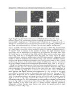
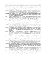
Fig. 9. Morphological evolution of structures on YBCO thin films induced by linear
polarized fs laser with fixed number of pulses N=600,000 and various fluences (a) F = 0
mJ/cm
2
, (b) F = 43 mJ/cm
2
, (c) F = 59 mJ/cm
2
, (d) F = 79 mJ/cm
2
, (e) F = 154 mJ/cm
2
, (f) F =
319 mJ/cm
2
. Inset: 2D Fourier spectra transferred from their corresponding SEM images (10
μm×10 μm with pixel resolution of ~0.04 nm). The scale bar is applied to all pictures.
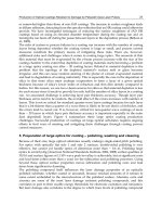
Figures 10(a)-10(c) show the evolution of the ripple structure on YBCO thin films irradiated
by a single-beam fs laser with various numbers of pulses (N) and the fixed laser fluence F =
79 mJ/cm
2
. With an increase in the number of pulses, the ripple structure became
increasingly clear in SEM images, as evidenced by the appearance of satellite peaks in the
2D Fourier spectra in the insets of Figs. 10(b) and 10(c) [there are no satellite peaks in the
inset of Fig. 10(a) for an as-deposited YBCO thin film]. The spatial period of ripples,
estimated from the position of satellite peaks in the 2D Fourier spectra, is independent of the
number of pulses or irradiation time, as shown in Fig. 11(b). Once the number of pulses ≧
50,000, i.e. the sample surface was irradiated by the 75 mJ/cm
2
laser pulses for ≧10 s, ripples
can be clearly observed on the surface of the sample. In addition, the real-time evolution of
the ripple structure appears in the transmission measurements in Fig. 10(d). In the case of F
= 154 mJ/cm
2
, the transmission power of the laser beam dramatically increased to within 2 s
and then saturated after ~10 s. Some specific points were marked at 79 mJ/cm
2
of Fig. 10(d),
and corresponding SEM images are shown in Figs. 10(a), 10(b), and 10(c), respectively. At
0.1 s [i.e. N=500 in Fig. 10(a)], there are almost no structures on the surface of YBCO thin
films. However, the rippled structure can be observed at 10 s [i.e. N=50,000 in Fig. 10(b)];
meanwhile, the transmission power dramatically increased due to the thinning of YBCO
films inside the grooves. For an extended irradiation time of 30 s [i.e. N=150,000 in Fig.
10(c)], the ripple structure does not change from that of Fig. 10(b), e.g. the spatial period of
ripple as shown in Fig. 11(b), except for the contrast of grooves causing slight rise in
transmission power in Fig. 10(d). Furthermore, the characteristics of changes in transmission
power in Fig. 10(d) are independent of laser fluence. This indicates that the formation of
ripple structures is very rapid, with only ~2 s needed, and the formation processes is
independent of laser fluence. Laser fluence only affects the spatial period of ripple
structures, as shown in Fig. 11(a).
Lasers – Applications in Science and Industry
12
Fig. 10. Morphological evolution of structures on YBCO thin films induced by linear
polarized fs laser with fixed laser fluence F = 79 mJ/cm
2
and various numbers of pulses (a)
N = 500, (b) N = 50,000, (c) N = 150,000. (d) The transmission power of laser pulses as a
function of irradiating time, i.e. pulse number N. Inset: 2D Fourier spectra which were
transferred from their corresponding SEM images (10 μm×10 μm with pixel resolution of
~0.04 nm). The scale bar is applied to all pictures.
Fig. 11. (a) Dependence of the ripple period on the fluence. (b) Dependence of the ripple
period on the number of pulses. The dashed lines are a guide to the eyes.
Nanoparticles and Nanostructures Fabricated Using Femtosecond Laser Pulses
13
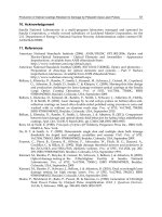
Fig. 12. Morphological evolution of ripple structures on YBCO thin films induced by linear
polarized fs laser with F = 300 mJ/cm
2
, N=150,000, and various incident angles (a) θ = 0°,
(b) θ = 30°, (c) θ = 60°. (d) Dependence of the ripple period on the incident angle of
laser pulses. The dashed lines are a guide to the eyes. All SEM images are 10 μm×10 μm
with pixel resolution of ~0.04 nm.
On the other hand, with the fluence and pulse number fixed at ~300 mJ/cm
2
and 150,000,
respectively, we found that the spatial period decreased with an increase in the incident
angle (θ) [see Fig. 12(d)]. However, the observed period of ripple at θ = 0° was significantly
smaller than the prediction of Λ=λ/(1+sinθ) (Zhou et al., 1982). In addition, the incident
angle-dependent period of ripples on YBCO thin films cannot be described using this
simplified scattering model [the solid line in Fig. 12(d)]. Therefore, the influence of surface
electromagnetic waves, i.e. surface plasmons (SPs) should be taken into account in the
formation of subwavelength ripples (Sakabe et al., 2009; Huang et al., 2009). According to
Shimotsuma’s et al. results (Shimotsuma et al.; 2003), femtosecond incident light easily
excites plasmons on the surface of various materials. As shown in Fig. 13(c), once the
momentum conservation condition for the wave vectors of the linear polarized laser light
(K
i
), the plasma wave (K
p
), and the laser-induced subwavelength periodic surface structures
(LIPSS, K
L
) is satisfied, such plasmons could couple with the incident light. The interference
between the plasmons and the incident light would generate a periodically modulated
electron density causing nonuniform melting. After irradiation with a femtosecond laser, the
interference ripple was inscribed on the surface of the YBCO thin film.
Lasers – Applications in Science and Industry
14
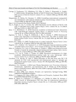
Fig. 13. SEM images (10 μm×10 μm with pixel resolution of ~0.04 nm) of fs LIPSS induced
by (a) the left- and (b) right-circularly polarized beams; (c) Schematic of the momentum
conservation condition of wave vectors of linear polarized laser light (K
i
), plasma wave (K
p
),
and LIPSS (K
L
); (d) Schematic processes of the LIPSS by circularly polarized laser light (K
i,C
).
The scale bar is applied to all pictures.
Interestingly, when we used a circularly polarized beam, the rippled structures were still
produced, as shown in Figs. 13(a) and 13(b). The orientation of the ripples was set at -45°
and +45° for left and right circularly polarized beams, respectively, with respect to the
incident plane of the beam. In both cases, the spatial period was 491 nm, as produced by fs
laser pulses with a fluence of 185 mJ/cm
2
and number of pulses set to 150,000. These results
show the orientation of rippled structures strongly depend on the polarization-state of
incident fs pulses. These results are consistent with the results of Zhao et al. on tungsten
(Zhao et al., 2007a, 2007b). In principle, circularly polarized light (K
i,c
) can be decomposed to
two perpendicular linear-polarization lights (E
x
and E
y
) through retardation of λ/4 in phase,
as shown in Fig. 13(d). Linearly polarized light E
x
and E
y
can induce the LIPSS K
L,x
and K
L,y
,
respectively, as long as the momentum conservation condition in Fig. 13(c) is satisfied. Thus,
both K
L,x
and K
L,y
with phase coherent further cause the K
L,c
according to the momentum
conservation condition of K
L,c
= K
L,x
+ K
L,y
. The 45° wave vector of LIPSS, K
L,c
, is completely
consistent with the direction of the satellite peaks in the 2D Fourier spectra [the inset of Fig.
13(a)]. Namely, the orientation of ripples is -45° for left-circularly polarized beams with
respect to the incident plane of the beam. Similarly, right-circularly polarized beams induce
a +45° orientation of LIPSS, K
L,c
, according to the momentum conservation condition of K
L,c
= -K
L,x
+ K
L,y
consistent with the results in Fig. 13(b).
Nanoparticles and Nanostructures Fabricated Using Femtosecond Laser Pulses
15
3.3 Generation of YBCO dot structures
To produce dot structures on YBCO thin films, we adopted a dual-beam scheme using the
modified Michelson interferometer shown in Fig. 14. The polarization of both beams was
individually controlled by two quarter-wave plates before the reflection mirrors in both
arms of the dual-beam setup. After the beam splitter in the dual-beam setup, both beams
were collinearly and simultaneously focused on the surface of the sample using a convex
lens with a focal length of 50-mm. Before generating the YBCO dot structures, we measured
the interference patterns between two beams to check the temporal overlap of the two
pulses. In the inset of Fig. 14, the interference pattern between the two pulses with parallel
polarization can be clearly observed after adjusting the delay in one of the two pulses. The
polarization of two pulses was set perpendicularly to each other to eliminate interference
patterns and generate the YBCO dot structures. All experiments were performed in air
under atmospheric pressure.
As shown in Figs. 15(a1)-15(d1), it is surprising that many dots rather than regular ripples
appeared on the surface of YBCO thin films using a dual-beam setup with perpendicularly
linear polarization. In the case of the dual-beam setup, the K
L,x
and K
L,y
without coherence
in phase induced by random phase and perpendicularly linear-polarization beams (E
x
and
E
y
), respectively, would not satisfy the conservation of momentum of K
L,c
= ±K
L,x
+ K
L,y
and
be unable to create ±45° wave vector of LIPSS, K
L,c
as shown in Fig. 13(d). Therefore, the K
L,x
and K
L,y
which are perpendicular to each other would lead 2D nonuniform melting and
further aggregation to form randomly distributed dots [see the 2D Fourier spectra in the
inset of Figs. 15(a2)-15(d2)] due to surface tension. In the case of N = 25,000, the average
diameter of dots was approximately 632 nm estimated by the log-normal fitting presented in
Fig. 15(a2). An increase in the number of pulses resulted in a marked broadening in the size
distribution, although the average size only slightly increased from 632 nm to 844 nm [see
Figs. 15(a2)-15(d2)]. For N = 300,000, the size of a part of dots was on the order of
micrometers. However, larger dots influence the dot density on the surface of YBCO thin
films. For instance, the density of dots increases with the number of pulses ≦150,000. Once
the dots grow too large to merge with the nearest neighbors, or even next nearest neighbors,
the density of the dots significantly shrank, as shown in Fig. 15(c1). In this manner, the size
and density of YBCO dots can be controlled by the numbers of pulses from the fs laser.
Fig. 14. Experimental setup for the generation of nanodots on YBCO thin films.
Lasers – Applications in Science and Industry
16
Fig. 15. Dot structures on YBCO thin films induced by a dual-beam setup with fluence = 87
mJ/cm
2
and various numbers of pulses (a1) N =25,000, (b1) N =50,000, (c1) N =150,000, (d1)
N =300,000. (a2)-(d2) The size distribution corresponds to the SEM images (10 μm×10 μm
with pixel resolution of ~0.04 nm) (a1)-(d1), respectively. Solid lines are the log-normal
fitting. Inset: 2D Fourier spectra which were transferred from their corresponding SEM
images (a1)-(d1), respectively. The scale bar is applied to all pictures.
3.4 Characteristics of YBCO nanostructures
To characterize the superconductivity of the ripple structures on YBCO thin films, the area
of the ripple structure must be large enough to measure. Thus, the scanning scheme shown
in Fig. 8 was adopted to prepare the large-area ripple structures on YBCO thin films. After
passing through a variable neutral density filter, the beam was two-dimensionally scanned
using a pair of galvanic mirrors with a speed of 7.6 cm/s. The laser beam was focused on the
surface of the sample with a spot size of 220 μm using an f-theta lens. All experiments were
performed in air under atmospheric pressure.
It is evident from Fig. 16(g) that the quality of the crystalline structure of the YBCO films
remained high after irradiation by the femtosecond laser with fluence up to 260 mJ/cm
2
.
However, the quality deteriorated considerably with a further increase in laser fluences. For
instance, with an irradiation fluence of 530 mJ/cm
2
, the intensity of the characteristic X-ray
diffraction peaks diminished considerably. As shown in Fig. 17, while the superconductivity
of the YBCO films remained nearly unchanged under low fluence irradiation, it began
degrading at irradiation levels of 320 mJ/cm
2
and disappeared at 530 mJ/cm
2
, indicating
structural and compositional changes with higher irradiation fluence.
Nanoparticles and Nanostructures Fabricated Using Femtosecond Laser Pulses
17
As mentioned above, the crystalline structure of these YBCO nanodots induced by the laser
irradiation (260 mJ/cm
2
) remained oriented with the c-axis, with sharp diamagnetic
Meissner effect characteristics at 89.7 K (Fig. 17), indicating that even after the dramatic
morphological reconstruction, the obtained nanodots maintained most of their intrinsic
properties. Indeed, as indicated by the energy dispersive spectroscopy (EDS) spectrum
displayed in Fig. 16(h), which was taken on one of the nanodots [marked as area 1 in Fig.
16(e)], the composition of the nanodot had not changed from that of the original YBCO
films. EDS results taken in the area between the dots [marked as area 2 in Fig. 16(e)]
indicates no signal of Ba. Instead, traces of Al, presumably from the LAO substrate, were
detected [see the second spectrum from the top in Fig. 16(h)]. This indicates that the
composition of the area between any two nanodots has severely deviated from the
stoichiometric composition of the original YBCO. The question is, how does this occur?
Fig. 16. (a) SEM images show the surface morphology of YBCO thin films at various laser
fluences (a) F = 0 mJ/cm
2
, (b) F = 210 mJ/cm
2
, (c) F = 320 mJ/cm
2
, (d) F = 530 mJ/cm
2
, (e) F
= 260 mJ/cm
2
. (f) AFM image of (e). (g) X-ray diffraction patterns of YBCO thin films at
various laser fluences corresponding to (a)-(e). (h) EDS spectra show the composition of area
1 and area 2 in (d) and (e).
Due to the laser pulses, the transient increase in temperature, ΔT, can be estimated using the
following relation ΔT = W / CV, where W is the pulse energy, C is the heat capacity, and V
is the illuminated volume. For YBCO at 300 K using C = 2.86×10
6
J/m
3
K [derived from the
Debye heat capacity and the Debye temperature of YBCO was obtained from ref. (Stupp &
Lasers – Applications in Science and Industry
18
Ginsberg, 1989)], V = 1.14×10
-14
m
3
(the absorption length ~ 300 nm), and W on the order of
0.1 mJ (which is assumed to be totally absorbed by YBCO). ΔT is approximately 3000 K. This
increase in temperature, in principle, will lead to massive global melting of a thin layer
beneath the surface of YBCO thin films. Thus, a more random pattern would be expected
when re-solidified. However, due to the interference induced by the inhomogeneous input
energy, the YBCO in melted phase initially forms ripples according to the interference
pattern which pushes the YBCO to the line of destructive interference. This interference
pattern also leads to a periodic distribution of the fluctuations in temperature, ΔT, which
happen to be higher than the boiling point of Ba [1897 K (Thompson & Vaughan, 2001)]
along the line of constructive interference and lower than the boiling point of Ba [1897 K
(Thompson & Vaughan, 2001)] along the line of destructive interference. As a result, in the
regions of the constructive interference most Ba was vaporized, while in the destructive
regions the Ba remained. Moreover, due to the surface tension and heterogeneous
nucleation on the surface of the substrate, the melted YBCO along the lines of destructive
interference aggregates to form nanodots in a periodic fashion, as shown in Fig. 16(b), 16 (e),
and 16(f). These results suggest that, by using single-beam femtosecond laser irradiation, it
is possible to fabricate a self-organized array of YBCO nanodots with most of the
crystallinity and superconducting properties remaining intact, provided proper control of
irradiation fluence is practiced. This technique could potentially be applied to the
fabrication of microwave filter devices with array structure or the weak-link Josephson
junction arrays.
Fig. 17. Resistance versus temperature curve measured prior to femtosecond laser
irradiation (F = 0 mJ/cm
2
) and the magnetization versus temperature curve measured at 10
Oe after femtosecond laser irradiation, with various fluences corresponding to the Fig. 16
(c), 16(d), and 16(e), respectively.
Nanoparticles and Nanostructures Fabricated Using Femtosecond Laser Pulses
19
Finally, as the fluence reached ≧ 320 mJ/cm
2
, irregular, disordered patterns were observed
on the surface of the LAO substrate, as shown in Fig. 16(c) and Fig. 16(d). The characteristic
XRD peaks of the (001)-YBCO films deteriorated significantly [Fig. 16(g)], indicating that the
crystalline structure of YBCO had been destroyed by the higher laser fluence. EDS analysis
[Fig. 16(h)] also shows that Ba was absent in both area 1 and area 2, marked in Fig. 16(d). In
area 2, even the composition of Y is absent in the EDS spectrum. Using the previous
estimation with W ≧ 0.12 mJ (fluence ≧ 320 mJ/cm
2
), ΔT ≧ 3700 K was obtained, which is
higher than the boiling point of Ba [1897 K (Thompson & Vaughan, 2001)] at the positions of
both constructive and destructive interference, but only higher than the boiling point of Y
[3345 K (Thompson & Vaughan, 2001)] at the position of constructive interference. In this
case, the aggregation of melted YBCO becomes more disordered and the stoichiometric
composition is more severely influenced, leading to the loss of crystalline integrity and
superconductivity in the remaining residue of the original YBCO film.
4. Conclusions
In this chapter, we demonstrated a simple, rapid means to obtain the hexagonal ZnSe
nanoparticles, YBCO ripples, and dot structures. In the fabrication of ZnSe nanoparticles,
while femtosecond laser pulses were focused on the surface of ZnSe wafers in air and the
ablated plume cannot expand as rapidly as plumes would in a vacuum chamber which
causes an instantaneous high-energy, high-pressure region around the focal point of the
laser; meanwhile, a large amount of spherical-shape ZnSe nanoparticles with an average
diameter of 16-22 nm (depending on the laser fluence) forms on the surface of the wafer.
During the formation of ZnSe nanoparticles, the structural phase further changes from cubic
to metastable hexagonal phase due to the ultrahigh localized ablation pressure caused by
the rapid injection of high laser energy within a femtosecond time scale.
For the generation of ripple and dot structures, we have systematically studied the surface
morphology of YBCO thin films under a single-beam and a dual-beam fs laser irradiation.
The generation of ripple and dot periodic structures was determined by the applied laser
fluence, number of pulses, and polarization of the laser. The period and orientation of
ripples, and even the size and density of dots can be controlled by these parameters. With
lower laser fluence, the (001)-YBCO film turns into (001)-ripple or dot arrays with
superconductivity remaining nearly intact. These rippled (or dotted) structures and
superconductivity, however, were rapidly destroyed with higher fluence. These results may
be applied to enhance the critical current of YBCO thin films and the fabrication of the
microwave filter devices with array structures or the weak-link Josephson junction arrays.
The present results clearly demonstrate that the femtosecond laser, in addition to its crucial
role in studying the ultrafast dynamics of matter, they can also serve as a new avenue for
engineering materials and structures into their surfaces at a nanometer scale.
5. Acknowledgments
The author would like to express his sincere appreciation and gratitude to his collaborators
and colleagues, Ms. H. I. Wang, Mr. W. T. Tang, Ms. C. C. Lee, and Mr. L. W. Liao, Profs. T.
Kobayashi, K. H. Wu, J. Y. Juang, J Y. Lin, T. M. Uen, C. S. Yang. This work was supported
by the MOE-ATU program at NCTU and National Science Council of Taiwan, under Grant
No. NSC 98-2112-M-009-008-MY3.
Lasers – Applications in Science and Industry
20
6. References
Amoruso, S.; Bruzzese, R.; Spinelli, N.; Velotta, R.; Vitiello, M.; Wang, X.; Ausanio, G.;
Lannotti, V. & Lanotte, L. (2004). Generation of Silicon Nanoparticles via
Femtosecond Laser Ablation in Vacuum. Applied Physics Letters, Vol.84, No.22,
(May 2004) pp. 4502-4504, ISSN 0003-6951
Batani, D.; Stabile, H.; Ravasio, A.; Lucchini, G.; Strati, F.; Desai, T.; Ullschmied, J.; Krousky,
E.; Skala, J.; Juha, L.; Kralikova, B.; Pfeifer, M.; Kadlec, Ch.; Mocek, T.; Präg, A.;
Nishimura, H. & Ochi, Y. (2003). Ablation pressure scaling at short laser
wavelength. Physical Review E, Vol.68, No.6, (December 2003) pp. 067403, ISSN
1539-3755
Bonse, J. & Krüger, J. (2010). Pulse Number Dependence of Laser-Induced Periodic Surface
Structures for Femtosecond Laser Irradiation of Silicon. Journal of Applied Physics,
Vol.108, No.3, (August 2010) pp. 034903, ISSN 0021-8979
Che, J.; Yao, X.; Jian, H. & Wang, M. (2004). Application and preparation of ZnSe nanometer
powder by reduction process. Ceramics International, Vol.30, No.7, (July 2004) pp.
1935-1938, ISSN 0272-8842
Dinger, A.; Becker, R.; Goppert, M.; Petillon S.; Grun, M.; Klingshirm, C.; Liang, J.; Wagner,
V. & Geurts, J. (2000). Lattice dynamical properties of cubic CdS/ZnSe strained-
layer superlattices. Journal of Crystal Growth, Vol.214, No.2, (June 2000) pp. 676-679,
ISSN 0022-0248
Groot, J. S. De; Estabrook, K. G.; Kruer, W. L.; Drake, R. P.; Mizuno, K. & Cameron, S. M.
(1992). Distributed absorption model for moderate to high laser powers. Physics of
Fluids B, Vol.4, No.3, (March 1992) pp. 701-707, ISSN 0899-8221
Greene, R. G.; Luo, H. & Ruoff, A. L. (1995). High pressure x-ray and raman study of ZnSe.
Journal of Physics and Chemistry of Solids, Vol.56, No.3/4, (March-April 1995) pp. 521-
524, ISSN 0022-3697
Hsu, E. M.; Crawford, T. H. R.; Tiedje, H. F. & Haugen, H. K. (2007). Periodic Surface
Structures on Gallium Phosphide after Irradiation with 150 fs–7 ns Laser Pulses at
800 nm. Applied Physics Letters, Vol.91, No.11, (September 2007) pp. 111102, ISSN
0003-6951
Huang, M.; Zhao, F.; Cheng, Y.; Xu, N. & Xu, Z. (2009). Origin of Laser-Induced Near-
Subwavelength Ripples: Interference between Surface Plasmons and Incident
Laser. ACS Nano, Vol.3, No.12, (November 2009) pp. 4062-4070, ISSN 1936-0851
Jiang, Y.; Meng, X. M.; Yiu, W. C.; Liu, J.; Ding, J. X.; Lee, C. S. & Lee, S. T. (2004). Zinc
Selenide Nanoribbons and Nanowires. The Journal of Physical Chemistry B, Vol.108,
No.9, (March 2004) pp. 2784-2787, ISSN 1520-6106
Jia, T. Q.; Zhao, F. L.; Huang, M.; Chen, H. X.; Qiu, J. R.; Li, R. X.; Xu, Z. Z. & Kuroda, H.
(2006). Alignment of Nanoparticles Formed on the Surface of 6H-SiC Crystals
Irradiated by Two Collinear Femtosecond Laser Beams. Applied Physics Letters,
Vol.88, No.11, (March 2006) pp. 111117, ISSN 0003-6951
Jia, X.; Jia, T. Q.; Zhang, Y,; Xiong, P. X.; Feng, D. H.; Sun, Z. R.; Qiu, J. R. & Xu, Z. Z. (2010).
Periodic Nanoripples in the Surface and Subsurface Layers in ZnO Irradiated by
Femtosecond Laser Pulses. Optics Letters, Vol.35, No.8, (April 2010) pp. 1248-1250,
ISSN 0146-9592
Nanoparticles and Nanostructures Fabricated Using Femtosecond Laser Pulses
21
Key, M. H.; Rumsby, P. T.; Evans, R. G.; Lewis, C. L. S.; Ward, J. M. & Cooke, R. L. (1980).
Study of Ablatively Imploded Spherical Shells. Physical Review Letters, Vol.45,
No.22, (December 1980) pp. 1801-1804, ISSN 0031-9007
Liu, B.; Hu, Z.; Che, Y.; Chen, Y. & Pan, X. (2007a). Nanoparticle generation in ultrafast
pulsed laser ablation of nickel. Applied Physics Letters, Vol.90, No. 4, (January 2007)
pp. 44103, ISSN 0003-6951
Liu, S. Y.; Choy, W. C. H.; Jin, L.; Leung, Y. P.; Zheng, G. P.; Wang, J. & Soh, A. K. (2007b).
Triple-Crystal Zinc Selenide Nanobelts. The Journal of Physical Chemistry C, Vol.111,
No.26, (July 2007) pp. 9055-9059, ISSN 1932-7447
Liu, S. Y.; Choy, W. C. H.; Jin, L.; Leung, Y. P.; Zheng, G. P.; Wang, J. & Soh, A. K. (2007).
Triple-Crystal Zinc Selenide Nanobelts. The Journal of Physical Chemistry C, Vol.111,
No.26, (July 2007) pp. 9055-9059, ISSN 1932-7447
Luo, C. W.; Lee, C. C.; Li, C. H.; Shih, H. C.; Chen, Y J.; Hsieh, C. C.; Su, C. H., Tzeng, W. Y.;
Wu, K. H.; Uen, T. M.; Juang, J. Y.; Chen, S. P.; Lin, J Y. & Kobayashi, T. (2008).
Ordered YBCO Sub-Micron Array Structures Induced by Pulsed Femtosecond
Laser Irradiation. Optics Express, Vol.16, No.25, (December 2008) pp. 20610-20616,
ISSN 1094-4087
Martienssen, W. & Warlimont, H. (2005). Springer Handbook of Condensed Matter and Materials
Data, Heidelberg: Springer-Verlag, Berlin
Nayak, B. K.; Gupta, M. C. & Kolasinski, K. W. (2008). Formation of Nano-Textured Conical
Microstructures in Titanium Metal Surface by Femtosecond Laser Irradiation.
Applied Physics A: Materials Science & Processing, Vol.90, No.3, (December 2007) pp.
399-402, ISSN 0947-8396
Okamuro, K.; Hashida, M.; Miyasaka, Y.; Ikuta, Y.; Tokita, S. & Sakabe, S. (2010). Laser
Fluence Dependence of Periodic Grating Structures Formed on Metal Surfaces
under Femtosecond Laser Pulse Irradiation. Physical Review B, Vol.82, No.16,
(October 2010) pp. 165417, ISSN 1098-0121
Rudolph, P.; Schäfer, N. & Fukuda, T. (1995). Crystal growth of ZnSe from the melt.
Materials Science and Engineering: R: Reports, Vol.15, No.3, (September 1995) pp. 85-
133, ISSN 0927-796X
Stupp, S. E. & Ginsberg, D. M. (1989). A review of the linear term in the low temperature
specific heat of YBa
2
Cu
3
O
7−δ
. Physica C Vol.158, No.3, (May 1989) pp. 299-310, ISSN
0921-4534
Stuart, B. C.; Feit, M. D.; Rubenchik, A. M.; Shore, B. W. & Perry, M. D. (1995). Laser-
Induced Damage in Dielectrics with Nanosecond to Subpicosecond Pulses. Physical
Review Letters, Vol.74, No.12, (March 1995) pp. 2248-2251, ISSN 0031-9007
Sarigiannis, D.; Peck, J. D., Kioseoglou, G.; Petrou, A. & Mountziaris, T. J. (2002).
Characterization of Vapor-Phase-Grown ZnSe nanoparticles. Applied Physics Letters,
Vol.80, No.21, (May 2002) pp. 4024-4026, ISSN 0003-6951
Shimotsuma, Y.; Kazansky, P. G.; Qiu, J. & Hirao, K. (2003). Self-Organized Nanogratings in
Glass Irradiated by Ultrashort Light Pulses. Physical Review Letters, Vol.91, No.24,
(December 2003) pp. 247405, ISSN 0031-9007
Shan, C. X.; Liu, Z.; Zhang, X. T.; Wong, C. C. & Hark, S. K. (2006). Wurtzite ZnSe
nanowires: growth, photoluminescence, and single-wire Raman properties.
Nanotechnology, Vol.17, No.22, (November 2006) pp. 5561-5564, ISSN 0957-4484
Lasers – Applications in Science and Industry
22
Sakabe, S.; Hashida, M.; Tokita, S.; Namba, S. & Okamuro, K. (2009). Mechanism for Self-
Formation of Periodic Grating Structures on a Metal Surface by a Femtosecond
Laser Pulse. Physical Review B, Vol.79, No.3, (January 2009) pp. 033409, ISSN 1098-
0121
Tseng, K. Y.; Wong, K. S. & Wong, G. K. L. (1996). Femtosecond Time-Resolved Z-scan
Investigations of optical nonolinearities in ZnSe. Optics Letters, Vol.21, No.3,
(February 1996) pp. 180-182, ISSN 0146-9592
Tawara, T.; Tanaka, S.; Kumano, H. & Suemune, I. (1999). Growth and luminescence
properties of self-organized ZnSe quantum dots. Applied Physics Letters, Vol.75,
No.2, (July 1999) pp. 235-237, ISSN 0003-6951
Thompson, A. C. & Vaughan, D. (2001). X-ray data booklet, Lawrence Berkeley National
Laboratory, California, USA
Tsuji, T.; Kakita, T. & Tsuji, M. (2003). Preparation of Nano-Size Particles of Silver with
Femtosecond Laser Ablation in Water. Applied Surface Science, Vol.206, No.1-4,
(February 2003) pp. 314-320, ISSN 0169-4332
Teng, Y.; Zhou, J.; Luo, F.; Ma, Z.; Lin, G. & Qiu, J. (2010). Shape- and Size-Controllable
Microstructure on Glass Surface Induced by Femtosecond Laser Irradiation. Optics
Letters, Vol.35, No.13, (July 2010) pp. 2299-2301, ISSN 0146-9592
Xiang, B.; Zhang, H. Z.; Li, G. H.; Yang, F. H.; Su, G. H.; Wang, R. M.; Xu, J.; Lu, G. W.; Sun,
X. C.; Zhao, Q. & Yu, D. P. (2003). Green-light-emitting ZnSe nanowires fabricated
via vapor phase growth. Applied Physics Letters, Vol.82, No.19, (May 2003) pp. 3330-
3332, ISSN 0003-6951
Yang, Y.; Yang, J.; Xue, L. & Guo, Y. (2010). Surface Patterning on Periodicity of
Femtosecond Laser-Induced Ripples. Applied Physics Letters, Vol.97, No.14, (October
2010) pp. 141101, ISSN 0003-6951
Zhou, G.; Fauchet, P. M. & Siegman, A. E. (1982). Growth of spontaneous periodic surface
structures on solids during laser illumination. Physical Review B, Vol.26, No.10,
(November 1982) pp. 5366-5381, ISSN 1098-0121
Zhao, Q. Z.; Malzer, S. & Wang, L. J. (2007a). Formation of subwavelength periodic
structures on tungsten induced by ultrashort laser pulses. Optics Letters, Vol.32,
No.13, (July 2007) pp. 1932-1934, ISSN 0146-9592
Zhao, Q. Z.; Malzer, S. & Wang, L. J. (2007b). Self-Organized Tungsten Nanospikes Grown
on Subwavelength Ripples Induced by Femtosecond Laser Pulses. Optics Express,
Vol.15, No.24, (November 2007) pp. 15741-15746, ISSN 1094-4087
2
Production of Optical Coatings Resistant to
Damage by Petawatt Class Laser Pulses
John Bellum
1
, Patrick Rambo, Jens Schwarz, Ian Smith,
Mark Kimmel, Damon Kletecka
1
and Briggs Atherton
Sandia National Laboratories, Albuquerque, NM
USA
1. Introduction
There are a number of ultra-high intensity lasers in operation around the world that
produce petawatt (PW) class pulses. The Z-Backlighter lasers at Sandia National
Laboratories belong to the class of these lasers whose laser beams are large (tens of cm) in
diameter and whose beam trains require large, meter-class, optics. This chapter provides an
in-depth overview of the production of state-of-the-art high laser-induced damage threshold
(LIDT) optical coatings for PW class laser pulses, with emphasis on depositing such coatings
on meter-class optics.
We begin with a review of ultra-high intensity laser pulses and the various approaches to
creating them, in order to establish the context and issues relating to high LIDT optical
coatings for such pulses. We next describe Sandia’s PW Z-Backlighter lasers as a specific
example of the class of large-scale lasers that generate PW pulses. Then we go into details of
the Sandia Large Optics Coating Operation, describing the features of the large optics
coating chamber in its Class 100 clean room environment, the coating process controls, and
the challenges in the production of high LIDT coatings on large dimension optical
substrates. The coatings consist of hafnia/silica layer pairs deposited by electron beam
evaporation with temperature control of the optical substrate and with ion assisted
deposition (IAD) for some coatings as a means of mitigating stress mismatch between the
coating and substrate. We continue with details of preparation of large optics for coating,
including the polishing and washing and cleaning of the substrate surfaces, in ways that
insure the highest LIDTs of coatings on those surfaces. We turn next to LIDT tests with
nanosecond and sub-picosecond class laser pulses while emphasizing the need, when
interpreting LIDT test results, to take into account the differences between the test laser
pulses and the pulses of the actual PW laser system. We present a comprehensive summary
of results of LIDT tests on Sandia coatings for PW pulses.
Two sections of the chapter present specific coating case studies, one for designs of a high
reflection (HR) coating with challenging performance specifications and one for the anti-
reflection (AR) coatings of a diagnostic beamsplitter. The coatings are for non-normal angle
1
Contract Associate to Sandia (JB with Sandia Staffing Alliance; DK with LMATA Government
Services)
Lasers – Applications in Science and Industry
24
of incidence (AOI), and the designs take into account behaviors of both S and P polarization
(Spol and Ppol) electric field intensities resulting from interference of forward and
backward propagating fields during reflection and transmission by the coatings. For the HR
coating, a 68 layer design and a 50 layer design both meet the stringent reflectivity
requirements (> 99.6% reflectivity of PW pulses in both Ppol and Spol over AOIs from 24
o
to
47
o
within ~ 1% bandwidth at both 527 nm and 1054 nm), but the 68 layer coating’s LIDT is
5 times less than that of the 50 layer coating because the electric field exhibits high intensity
peaks deep within the former coating, but exhibits peaks of moderate intensity that quench
rapidly into the latter coating. The study of the AR coatings features measurements of their
reflectivities, and of their uniformity over the 92 cm dimension of test optics in the coating
chamber. The final section of the chapter presents a conclusion.
2. Ultra-high intensity laser pulses and approaches to creating them
Many ultra-high intensity laser facilities are in operation or under development around the
world. Information on these facilities has been compiled by The International Committee on
Ultra-High Intensity Lasers (ICUIL) and is available on its website, www.icuil.org. Such high
intensity lasers are opening up an ever widening scope of research into laser-matter
interactions beyond linear and non-linear optical phenomena at the level of molecular
electronic structure and excitation to production of high energy density plasmas, energetic x-
rays, inertial confinement fusion and laser induced acceleration of electrons and ions up to
relativistic speeds (Perry & Mourou, 1994; Mourou & Umstadter, 2002; Tajima et al., 2010;
Mourou & Tajima, 2011). Ultra-high intensity lasers depend on methods of creating laser
pulses either of large energy per pulse, or of short pulse duration, or both. By large pulse
energies we mean in the range from J to MJ but typically in the kJ regime for a single laser
beam train; and by short pulse durations we mean in the ns, ps, fs or shorter regimes. Actually,
in the world of ultra-high intensity lasers, reference to “long” in terms of pulse duration means
ns class pulses; and “short” means sub-ns class pulses. The resulting intensities of these laser
pulses are typically terawatt (TW) to PW and even higher. Focusing of the beams leads to
corresponding fluences of 10
16
W/cm
2
to 10
19
W/cm
2
and beyond, approaching 10
22
W/cm
2
,
depending on the particular laser system and on the achievable minimum focal spot size.
Aberrations prevent focusing in the diffraction limit, so minimizing beam train aberrations is
critical to achieving the highest fluences at focus. On the other hand, defocusing the beam in a
controlled way is sometimes useful as a means of lowering the fluence to some specific level
within a focal spot larger than the minimum achievable one.
Regardless of a laser’s pulse duration/energy combination, its practical and optimal
operation is feasible only to the extent that the laser pulses can traverse the beam train
without causing damage or aberrations to its components (windows, mirrors, lenses, gain
media, etc.) or their optical coatings. Such laser-induced damage has been the focus of
extensive research (Wood, 1990, 2003). It can result from any linear or non-linear laser-
matter interaction and is characterized by its LIDT, the laser fluence at or above which it
occurs. Optical coatings are our particular concern, and we will deal with both HR and AR
types in this chapter. HR and AR coatings are, like optical coatings in general, specific to
their use wavelengths, which are the wavelengths of the ultra-high intensity lasers in this
context. AR coatings consist of a few (usually < 10) alternating high and low index of
refraction thin film layers while HR coatings consist of typically a few tens (< 40) of such
layers. They serve the crucial role of reducing loss of energy of the laser pulses in the beam
Production of Optical Coatings Resistant to Damage by Petawatt Class Laser Pulses
25
train; in the case of AR coatings, by minimizing reflection losses at the surfaces of
transmissive optics (i. e., windows or lenses) through which the pulses propagate; and, in
the case of HR coatings, by minimizing transmission losses (i.e., by providing excellent
reflectivities) at the surfaces of mirrors that reflect the pulses. In any case, unless these
coatings as well as the optics of a laser beam train can resist damage and aberrations
induced by the laser’s pulses, the high energy, high intensity pulses of light will not arrive at
their final focal volume efficiently enough to reach the fluence levels that produce the ultra-
high energy density laser-matter interactions of interest.
The main approaches in creating ultra-high intensity laser light are as follows.
2.1 Laser systems with beam trains of large dimension and cross section
These lasers, owing to the distribution of the pulse energy over large beam cross sectional
areas, can generate and handle pulses of large energies at fluences below the LIDTs of the
laser optics and coatings. Such lasers, of which there about 15 around the world according to
the ICUIL website, www.icuil.org, depend on major government support to provide the
large facilities and infrastructure they require. They face the challenges and costs of
fabricating and coating large dimension optics to high optical precision. The costs start
becoming prohibitive at optic dimensions approaching a meter and beyond, especially for
parabolic or other non-planar, non-spherical polished surfaces. But, because energy capacity
per pulse increases linearly with beam cross sectional area, up to 4 orders of magnitude
increase in pulse energies are possible in going from table top lasers with cm class beam
trains to large scale lasers with meter class beam trains. Meter class laser beam trains can
support kJ class energies per pulse. Perhaps the most well known of this class of lasers are
the National Ignition Facility (NIF) laser system, comprised of 192 laser beam trains, at
Lawrence Livermore National Laboratory (LLNL) in the United States
( and the Laser MegaJoule (LMJ) laser system, comprised of 240
laser beam trains, at the Commissariat a l’Energie Atomique in France (http://www-
lmj.cea.fr/).
2.2 Implementation of gain media, optics and coatings with superior resistance to
laser-induced damage or aberrations
High LIDT gain media, optics and optical coatings are the focus of important, on-going
research. Gains in energy capacity per pulse of a given laser system due to improvements in
the LIDTs of optics and coatings can be significant, amounting to factors of 2 or more, but
usually less than 10. As mentioned, laser-induced aberrations within gain media and optics
undermine the achievement of ultra-high intensities by causing distortion of the beam’s
wave front and corresponding decrease of its fluence at focus. This latter effect can easily
spoil the focal fluence by 1 or 2 orders of magnitude. Most ultra-high intensity lasers utilize
optics and gain media with the highest fluence thresholds for laser-induced aberrations and
operate at energies per pulse up to but not beyond those thresholds. They then use spatial
filtering to restore the wave front of the high energy beam back closer to what it was at
lower pulse energy. But, regardless of the optical medium, as laser intensities become higher
and higher, the laser-induced aberrations eventually lead to local run-away self-focusing
and catastrophic damage along fine, filament-like pathways (Perry & Mourou, 1994). This is
due to an accumulation (referred to as the B integral) of laser-induced non-linear optical
phase distortions along the propagation path, and correlates especially with intensity hot
Lasers – Applications in Science and Industry
26
spots that are not uncommon in the cross section of high intensity laser beams. Fused silica
and BK7 are among the most laser damage resistant optical grade glasses (Wood, 2003), and
Nd:Phosphate Glass and Ti:Sapphire are laser gain media that also exhibit high fluence
thresholds for laser-induced damage (Wood, 2003) and at the same time afford some of the
highest energy storage capacities (Perry & Mourou, 1994), at the optimal wavelengths of
1054 nm in the former case and 800 nm in the latter case. Ti:Sapphire can, however, also
provide reasonable energy storage and lasing over a broad spectral range. As to thin film
optical coatings, LIDTs depend not only on the coating materials but also on the coating
design, on the techniques of preparing the optics for coating, and on the coating process
itself. We will treat issues of coating design in more detail in this chapter. Regarding the
polishing and preparing of optics for coating, we have demonstrated in the case of an AR
coating that using one combination of polishing compound and wash preparation for the
substrate prior to coating over another can lead to an improvement by a factor of 2 in the
laser damage threshold of the coating, and hence the energy capacity per pulse of the laser
(Bellum et al., 2010).
2.3 Methods of generating laser pulses of ever shorter duration
For a given energy per pulse, the intensity of the laser light varies inversely with pulse
duration. So, techniques such as Q-switching or mode locking to produce short laser pulses,
of ns, ps, fs, or even shorter durations, without appreciably reducing the energy per pulse,
can lead to orders of magnitude increases in laser intensities.
All ultra-high intensity laser systems involve trade-offs between the above 3 approaches.
Avoiding self-focusing is a major factor in any laser design. It not only limits the thicknesses
of gain media and optics for given laser pulse energies and durations, but also prevents sub-
ns class laser pulses produced by means of laser cavity based techniques such as Q-
switching and mode locking from being able to undergo effective amplification in high
energy capacity solid state gain media like Ti:Sapphire and Nd:Phosphate Glass. The reason
for this latter limitation is that sub-ns pulses, as they increase in energy per pulse, reach the
fluence levels resulting in self-focusing before they reach the saturation fluences necessary
for efficient extraction of stored energy in the gain medium (Perry & Mourou, 1994). Due to
this, the successful ultra-high intensity laser systems developed during the first few decades
after the advent of the laser in the 1960s were based on approaches 2.1 and 2.2 above
featuring ns class pulses. These were large laser systems using solid state gain media and
generating kJ per pulse class laser beams of large, meter class dimensions, and were the
predecessors of the NIF and LMJ class of lasers.
The advent of chirped pulse amplification (CPA) in the mid 1980s was a major breakthrough
in opening up the realm of sub-ns ultra-high intensity laser pulses (Perry & Mourou, 1994;
Strickland & Mourou, 1985; Maine et al., 1988). CPA technology uses optical gratings or
other optical techniques to “stretch” a low energy sub-ps class laser pulse of sufficient
bandwidth into a ps to ns class pulse, which can then undergo efficient amplification
without the self-focusing problems that would occur for the sub-ps class pulse. A reverse
version of the “stretching” process then recompresses the amplified ps to ns class pulse into
a high energy, sub-ps class pulse. Focusing of these high energy laser pulses is the final step
in achieving the ultra-high fluences of coherent light and their associated electric and
magnetic optical fields that in turn lead to the high energy density laser-matter interactions.
CPA with ps and fs class pulses has permitted the development of ultra-high intensity table
Production of Optical Coatings Resistant to Damage by Petawatt Class Laser Pulses
27
top lasers, but is also a technique that has become more and more common in the context of
the large, meter-class, ultra-high intensity laser systems, taking them from ns pulses at TW
intensity levels with 10
18
J/cm
2
to sub-ps pulses at PW intensity levels with > 10
21
J/cm
2
.
3. The Sandia TW and PW Z-Backlighter lasers
The Z-Backlighter lasers at Sandia National Laboratories are part of the Pulsed Power
Sciences program ( in support of the Z-Accelerator,
which produces extremely high energy density conditions by means of a magnetic pinch
along the vertical (Z) direction, and is the most powerful source of x-rays in the world.
There are two basic Z-Backlighter lasers, Z-Beamlet (Rambo et al., 2005) with TW, ns class
pulses and Z-Petawatt (Schwarz et al., 2008) with 100 TW up to PW, sub-ps class pulses.
These pulses, after propagating nearly 200 feet from the Z-Backlighter Laser Facility to the
Z-Accelerator, undergo focusing onto target foils near the Z pinch. Their focused fluences,
ranging from 10
16
to 10
20
W/cm
2
, produce highly energetic x-rays that back-light the
magnetic pinch with enough energy to penetrate its high energy density core and, in this
way, provide a diagnostic of the pinch as it occurs (Sinars et al., 2003).
The ns class Z-Beamlet laser pulses undergo multi-pass power amplification in Xe flashlamp
pumped Nd:Phosphate Glass amplifier slabs at 1054 nm laser wavelength corresponding to
the fundamental laser frequency of Nd:Phosphate Glass. Z-Beamlet then converts these
amplified pulses by means of frequency doubling in a large dimension KDP crystal to the
second harmonic at 527 nm. Its pulses are of duration in the range 0.3 – 8 ns, but the most
common operation is with 1 – 2 ns pulses, and pulse energies of up to ~ 2 kJ at 527 nm in a
beam of about 900 cm
2
cross sectional area. The sub-ps class Z-Petawatt laser uses optical
parametric chirped pulse amplification (OPCPA). A Ti:Sapphire laser operating at 1054 nm
provides 100 fs pulses at low (nJ) energies. A double-pass grating stretcher temporally
expands these pulses to ~ 2 ns duration. The stretched pulses then undergo optical
parametric amplification (OPA) in three stages, by means of a BBO crystal in each stage
pumped by amplified, ~ 2 ns pulses at 532 nm of a frequency doubled Nd:YAG laser. After
amplification in double-pass rod amplifiers, the OPA output pulses undergo final double-
pass amplification in the main amplifier consisting of 10 Xe-flashlamp pumped
Nd:Phosphate Glass slabs (44.8 cm X 78.8 cm X 4.0 cm). The output pulses from the main
amplifier then are temporally compressed to ~ 500 fs by means of large, meter class gratings.
The Z-Petawatt output pulses can range in duration down to ~ 500 fs and the energies per
pulse can extend up to ~ 420 J in the current configuration that uses gratings produced on
gold coated meter-class fused silica substrates. New gratings have now been produced for
Sandia by Plymouth Grating Laboratory (www.plymouthgrating.com) by means of a laser
based nano-ruler process (Smith et al., 2008) on large (94 cm X 42 cm X 9 cm) fused silica
substrates which, prior to the nano-ruler process, were coated by Sandia with a multi-layer
dielectric (MLD) coating. These new MLD gratings will permit energies per sub-ps pulse
approaching 1 kJ due to their superior resistance to laser damage as compared to that of the
gratings on the gold coated substrates. The expanded Z-Beamlet laser beam can present 2.5 –
10 J/cm
2
in a 1 ns pulse of 527 nm light over its cross section. In the case of the Z-Petawatt
laser, the beam can present 1 - 2 J/cm
2
in a 700 fs pulse of 1054 nm light over its cross
section. Our goal in large optics coatings is that their LIDTs exceed these fluences, and
preferably by factors of ~ 2 in order to handle hot spots in the beams.
Lasers – Applications in Science and Industry
28
4. Depositing high LIDT coatings at Sandia’s large optics coating operation
Coating large optics goes hand in hand with large vacuum coating chambers. In Sandia’s
case, the coating chamber is 2.3 m x 2.3 m x 1.8 m in size and opens to a Class 100 clean
room equipped for handling and cleaning the large optics for coating (see Fig. 1). Such a
highly clean environment, with downward laminar air flow into a perforated raised floor to
enhance the laminar quality, is critically important to the production of optical coatings
exhibiting the highest possible LIDTs. This is due to the fact that even nano-scale
particulates on an optical surface prior to coating become initiation sites for laser damage of
the coated surface to occur at lower LIDTs (Stolz & Genin, 2003). A major issue with
particulates is that, when the coating chamber is not under vacuum and its door is open,
coating material on the chamber walls tends to flake off, violating Class 100 conditions
inside and in front of the chamber. This calls for measures to prevent these particulates from
contaminating the surfaces of product optics prior to coating. One such measure is the use of
clean room curtains, as shown in Fig. 1, to separate the area in front of the coater from the
rest of the Class 100 area, shown in Fig. 2, in which optics undergo cleaning and preparation
for coating. Another such measure is to handle optics in preparation for coating and to load
them into the chamber using special tooling and techniques that protect the surfaces
undergoing coating from exposure to the non-Class 100 conditions in front of and inside the
open chamber. Once the chamber door is closed, the downward laminar flow of Class 100
air quickly restores the area in front of the chamber to Class 100 status; and the risks of
particle contamination inside the chamber are negligible when it is under vacuum.
Fig. 1. The Sandia large optics coating chamber and process control console.
Production of Optical Coatings Resistant to Damage by Petawatt Class Laser Pulses
29
Among deposition methods that produce high quality coatings, conventional electron beam
(e-beam) evaporation of thin film materials is the most suitable for coating large optical
substrates. This is because of the high levels of uniformity of the coating over large substrate
areas that are achievable with e-beam deposition due, in part, to the relatively large cone
angles of the plumes of e-beam evaporated coating molecules. In addition, motion of the
substrates in planetary fixtures as well as masks with special design and placement between
the thin film material sources and the substrates are necessary as a means of controlling and
averaging out the deposition to insure uniform thin film layer thicknesses. In Sandia’s 3-planet
configuration, as shown in Fig. 3, each planetary fixture can hold optical substrates up to 94 cm
in diameter. The planet fixtures of a 2-planet, counter-rotating option, can hold substrates up
to 1.2 m in one dimension and 80 cm in the other. The coater has three e-beam sources (see Fig.
3) for evaporation of the thin film materials. Hafnia and silica are, respectively, the high and
low index of refraction layers of choice for high LIDT coatings, due to their high resistance to
laser damage by visible and near infra-red light (Fournet et al., 1995; Stolz & Genin, 2003; Stolz
et al., 2008). Crystal sensors in locations on the bottom sides of the masks, which are near the
plane of the optical surfaces undergoing coating, serve to monitor the coating process by
detecting the amount and rate at which they accumulate coating material during deposition.
The Sandia chamber also can accommodate optical monitoring of the coating deposition
process. An RF ion source (see Fig. 3) provides the option of IAD. The base pressure of the
coating chamber needs to be ~ 1 – 2 X 10
-6
Torr in order to insure contamination free conditions
for the deposition process.
Fig. 2. Sandia’s Class 100 clean room for washing and preparing large optics for coating.
Achieving high LIDT coatings depends not only on use of coating materials with high
resistance to laser damage, but also on the methods of preparing the substrate surfaces for
coating and on the deposition processes and process control, as we mentioned above, and,
as we will see later in the chapter, on the coating design. Direct e-beam evaporation of silica,
Lasers – Applications in Science and Industry
30
because it occurs at moderate e-beam current and voltage, leads to generally defect-free thin
film layers. This is, however, not the case for hafnia because it requires much higher e-beam
current and voltage to evaporate, which in turn increases the risk of the evaporation process
producing hafnia particulates along with hafnia molecules. Such particulates that attach to
the coating as it is forming become defect sites that can initiate laser damage. To avoid this,
we use direct e-beam evaporation of hafnium metal in combination with a back pressure of
oxygen at ~ 10
-4
Torr that is sufficient to insure that all of the evaporated hafnium atoms
react with oxygen to form hafnia molecules that then form the hafnia coating layer. This
occurs in a defect-free way because evaporation of hafnium metal occurs at more moderate
e-beam current and voltage than evaporation of hafnia, with correspondingly lower risk of
producing particulates in the evaporation process.
Fig. 3. Interior of the Sandia large optics coating chamber.
A feature of the Sandia large optics coater is the control of the substrate temperature - that is,
the temperature within the coating chamber - during deposition. The temperature governs the
energy of molecular motion, both of the coating molecules as they assemble to form a coating
layer and of the substrate molecules in their phonon degrees of freedom. Thus, lowering or
raising the temperature can change the dynamics at the molecular level by which coatings
form. In particular, coating at an elevated temperature of ~ 200
o
C can promote formation of
coatings with mechanical stress (Strauss, 2003) that matches or is close to that of the substrate.
This is important because stress differences between a coating and substrate increase the risk
of the coating delaminating from the substrate. The case of HR coatings on BK7 optical glass is
a good example of how deposition at ~ 200
o
C results in low stress differences between coating
and substrate. With IAD, ions from the ion source bombard the coating layer as it forms, thus
modifying how the coating molecules assemble into a layer. Such IAD coatings are usually
denser with a higher level of surface roughness, and have less stress mismatch with the
substrate, than do non-IAD e-beam deposited coatings, and their LIDTs tend to be as high as