Heat Transfer Engineering Applications Part 2 docx
Bạn đang xem bản rút gọn của tài liệu. Xem và tải ngay bản đầy đủ của tài liệu tại đây (2.09 MB, 30 trang )
Mathematical Models of Heat Flow in Edge-Emitting Semiconductor Lasers 17
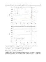
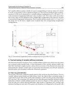
Fig. 13. Transverse temperature profiles at the front facet of the central emitter. Dashed
vertical lines indicate the edges of heat spreader and substrate.
where Θ
(t)=1 or 0 exactly reproduces the driving current changes.
7. Heat flow in a quantum cascade laser
Quantum-cascade lasers are semiconductor devices exploiting superlattices as active layers.
In numerous experiments, it has been shown that the thermal conductivity λ of a superlattice
19
Mathematical Models of Heat Flow in Edge-Emitting Semiconductor Lasers
18 Will-be-set-by-IN-TECH
Fig. 14. Calculated c ross-plane thermal conductivity for the active region of THz
QCL (Szyma´nski ( 2011)). Square symbols show the values measured by Vitiello et al. (2008).
is significantly reduced (Capinski et al. (1999); Cahill et al. (2003); Huxtable et al. (2002)).
Particularly, the cross-plane value λ
⊥
may be even order-of-magnitude s maller than than
the val ue for constituent bulk materials. The phenomenon is a serious problem for Q CLs,
since they are electrically pumped by driving voltages over 10 V and current densities over
10 kA/cm
2
. Such a high injection power densities lead to intensive heat generation inside the
devices. To make things worse, the main heat sources are located in the active layer, where
the density of interfaces is the highest and—in consequence—the heat removal is obstructed.
Thermal management in this case seems to be the key problem in design of the improved
devices.
Theoretical description of heat flow across SL’s i s a really hard task. The crucial point is finding
the relation between phonon m ean free path Λ andSLperiodD Yang & Chen (2003). In case
Λ
> D, both wave- and particle-like phonon behaviour is observed. The thermal conductivity
is calculated through the modified phonon dispersion relation obtained from the equation of
motion of atoms i n the crystal lattice (see f or example Tamura et al. (1999)). In case Λ
<
D, phonons behave like particles. The thermal conductivity is usually calculated using the
Boltzmann transport equation with boundary conditions involving diffuse scattering.
Unfortunately, using the described methods in the thermal model of QCL’s is questionable.
They are very complicated on the one hand and often do not provide satisfactionary results
on the other. The comprehensive comparison of theoretical predictions with experiments for
20
Heat Transfer - Engineering Applications
Mathematical Models of Heat Flow in Edge-Emitting Semiconductor Lasers 19
nanoscale heat transport can be found in Table II in Cahill et al. (2003). This topic was also
widely discussed by Gesikowska & Nakwaski (2008). In addition, the investigations in this
field usually deal with bilayer SL’s, while one period of QCL active layer consists of dozen or
so layers of order-of-magnitude thickness differences.
Consequently, present-day mathematical models of heat flow in QCLs resemble those created
for standard edge emitting lasers: they are based on heat conduction equation, isothermal
condition at the bo ttom of the structure and convective cooling of the top and side walls are
assumed. QCL’s as unipolar devices are not affected by s urface recombination. Their mirrors
may be hotter than the inner part of resonator only due to bonding imperfections (see 8.4).
Colour maps showing temperature in the QCL cross-section and illustrating fractions of heat
flowing through particular surfaces can be found in Lee et al. (2009) and Lops et al. (2006). In
those approaches, the SL’s were replaced by equivalent layers described by anisotropic values
of thermal conductivity λ
⊥
and λ
arbitrarily reduced (Lee et al. (2009)) or treated as fitting
parameters (Lops et al. (2006)).
Fig. 15. Illustration of significant discrepancy between values of λ
⊥
measured by Vitiello et
al. (2008) and calculated according to equation (20), which neglects the influence of
interfaces (Szyma ´nski (2011)).
Proposing a relatively simple method of assessing the thermal conductivity of QCL active
region has been a subject of several works. A very interesting idea was mentioned by Zhu et
al. (2006) and developed by Szyma ´nski (2011). The method will be briefly described below.
21
Mathematical Models of Heat Flow in Edge-Emitting Semiconductor Lasers
20 Will-be-set-by-IN-TECH
The thermal conductivity of a multilayered structure can be approximated according to the
rule of mixtures Samvedi & To mar (2009); Zhou et al. (2007):
λ
−1
=
∑
n
f
n
λ
−1
n
, (20)
where f
n
and λ
n
are the volume fraction and bulk thermal conductivity of the n-th material.
However, in case of high density of interfaces, the approach (20) is inaccurate because of
the following reason. The interface between materials of different thermal and m echanical
properties obstructs the heat flow, introducing so called ’Kapitza resistance’ or thermal
boundary resistance (TBR) Swartz & Pohl (1989). The phenomenon can be described by
two phonon scattering models, namely the acoustic mismatch model (AMM) and the diffuse
mismatch model (DMM). Input data are limited to such basic material parameters like Debye
temperature, density or acoustic wave speed. Thus, the thermal conductivity of the QCL
active region can be calculated as a sum of weighted average of constituent bulk materials
reduced by averaged TBR multiplied by the number of interfaces:
λ
−1
⊥
=
d
1
d
1
+ d
2
r
1
+
d
2
d
1
+ d
2
r
2
+
n
i
d
1
+ d
2
r
(av)
Bd
, (21)
where TBR has been averaged with respect to the direction of the heat flow
r
(av)
Bd
=
r
Bd
(1 → 2)+r
Bd
(2 → 1)
2
. (22)
The detailed prescription on how to calculate r
(av)
Bd
can be found in Szyma´nski (2011).
The model based on equations (21) and (22) was positively tested on bilayer
Si
0.84
Ge
0.16
/Si
0.74
Ge
0.26
SL’s investigated experimentally by Huxtable et al. (2002). Then,
GaAs/Al
0.15
Ga
0.85
As THz QCL was considered. Results of calculations exhibit good
convergence with measurements presented by V itiello et al. (2008) as shown in Fig. 14. On
the contrary, values of λ
⊥
calculated according to equation (20), neglecting the influence of
interfaces, show significant d iscrepancy with the m easured ones (Fig. 15).
8. Summary
Main conclusions or hints dealing with thermal models of edge-emitting lasers will be
aggregated in the form of the following paragraphs.
8.1 Differential equations
A classification of thermal models i s presented in Table 4. Basic thermal behaviour of an
edge-emitting laser can be described according to A pproach 1. It is assumed that the heat
power is generated uniformly in selected regions: mainly in active layer and, in minor
degree, in highly resistive layers. Considering the laser cross-section parallel to mirrors’
surfaces and reducing the dimensionality of the heat conduction equation to 2 is fully
justified. For calculating the temperature in the entire device (including the vicinity of
mirrors) Approach 2 should be used. The main heat s ources may be determined as functions
of carrier concentration calculated from the diffusion equation. It is recommended to use
three-dimensional heat conduction equation. The diffusion equation can be solved in the
22
Heat Transfer - Engineering Applications
Mathematical Models of Heat Flow in Edge-Emitting Semiconductor Lasers 21
Approach Equations(s) Calculated T Application Example references
inside the
resonator
in the vicinity
of mirrors
1 HC yes near-threshold
regime
basic thermal beha-
viour of a l a ser
Joyce & Dixon (1975),
Puchert et al. (1997),
Szyma´nski et al.
(2007)
2 HC+D yes low-power
operation
thermal behaviour
of a laser
including the
vicinity of
mirrors
Chen & Tien (1993),
Mukherjee &
McInerney (2007)
3 HC+D+PR yes high-power
operation
facet temperature
reduction
Romo et al . (2003)
Table 4. A classification of thermal models. Abbreviations: HC-heat conduction, D-diffusion,
PR -photon rate.
plane of junction (2 dimensions) or reduced to the axial direction (1 dimension). Approach 3
is the most advanced one. It is based on 4 differential equations, which should be solved in
self-consisted loop (see Fig. 9). Approach 3 is suitable for standard devices as well as for lasers
with modified close-to-facet regions.
8.2 Boundary conditions
The following list presents typical boundary conditions (see for example Joyce & Dixon
(1975), Puchert et al. (1997), Szyma´nski e t al. (2007)):
— isothermal condition at the bottom of the device,
— thermally insulated side walls,
— convectively cooled or thermally insulated (which is the case of zero convection
coefficient) upper surface.
In Szyma´nski (2007), it was shown that assuming isothermal condition at the upper surface is
also correct and reveals better convergence with experiment.
Specifying the bottom of the device may be troublesome. Considering the heat flow in the chip
only, i.e. assuming the ideal heat sink, leads to significant errors (Szyma ´nski et al. (2007)).
On the other hand taking into account the whole assembly (chip, heat spreader and heat
sink) is difficult. In the case of analytical approach, it significantly complicates the geometry
of the thermal scheme. In order to avoid that tricky modifications of thermal scheme (like
in Szyma´nski et al. (2007)) have to be introduced. In case of numerical approach, using
non-uniform mesh is absolutely necessary (see for example Puchert et al. (2000)).
In Ziegler et al. (2006), an actively cooled device was investigated. In that case a very strong
convection (α
= 40 ∗ 10
4
W/(mK )) at the bottom surface was assumed in calculations.
8.3 Calculation methods
Numerous works dealing with thermal modelling of edge-emitting lasers use analytical
approaches. Some of the m exploit highly sophisticated mathematical methods. For example,
23
Mathematical Models of Heat Flow in Edge-Emitting Semiconductor Lasers
22 Will-be-set-by-IN-TECH
Kirchhoff transformation (see Nakwaski (1980)) underlied further pioneering theoretical
studies on the COD process by Nakwaski (1985) and Nak waski (1990), where s olutions
of the three-dimensional time-dependent heat conduction equation were found using the
Green function formalism. Conformal mapping has be en used by Laikhtman et al. (2004)
and L aikhtman e t al. (2005) for thermal optimisation of high power diode laser b ars. Relatively
simple separation-of-variables approach was used by Joyce & Dixon (1975) and developed in
many further works (see for example Bärwolff et al. (1995) or works by the author of this
chapter).
Analytical models often play a very he lpful role in fundamental understanding o f the device
operation. Some people appreciate their beauty. However, one should keep in mind that
edge-emitting d evices are frequently more complicated. This statement deals with the internal
chip structure as well as packaging details. Analytical solutions, which can be found in
widely-known textbooks (see for example Carslaw & Jaeger (1959)), are usually developed
for regular figures like rectangular or cylindrical rods made of homogeneous materials. Small
deviation from the co nsidered geometry often l eads to substantial changes in the solution. In
addition, as far as solving single heat conduction equation in some cases may be relatively
easy, including other equations enormously complicates the problem. Recent development
of simulation software based on Finite Element Method creates the temptation to relay on
numerical methods. In this chapter, the commercial software has been used for computing
dynamical temperature profiles (Fig. 12 and 13)
9
and carrier concentration profiles (Fig. 7
and 8).
10
Commercial software was also used in many works, see for example Mukherjee
& McInerney ( 2007); Puchert et al. (2000); Romo et al. (2003). In Ziegler et al. (2006; 2008),
a self-made software based on FEM provided results highly convergent with sophisticated
thermal measurements of high-power diode lasers. Thus, nowadays numerical m ethods seem
to be more appropriate for thermal analysis of modern edge-emitting devices. However, one
may expect that analytical models will not dissolve and remain as helpful tools for crude
estimations, verifications of numerical results or fundamental understanding of particular
phenomena.
8.4 Limitations
While using any kind of model, one should be prepared for unavoidable inaccuracies of the
temperature calculations caused by factors characteristic for individual devices, which elude
qualitative as sessment. The paragraphs below briefly describe each factor.
Real solder layers may contain a number of voids, such as inclusions of air, clean-up agents
or fluxes. Fig. 12 in Bärwolff et al. (1995) shows that small voids in the solder only slightly
obstruct the heat removal from the laser chip to the he at sink unless their concentration is ve ry
high. In turn, the influence of one large void is much bigger: the device thermal resistance
grows nearly linearly with respect to void size.
The laser chip m ay not adhere t o the heat sink entirely due to two reasons: the metallization
may not e xtend exactly t o the laser facets or the chip can be inaccurately bonded (it can extend
over the heat sink edge). In Lynch (1980), it was shown that such an overhang may contribute
to order of magnitude increase of the device thermal resistance.
9
CFDRC software ( used used by Zenon Gniazdowski.
10
FlexPDE software ( used by Michal Szyma´nski.
24
Heat Transfer - Engineering Applications
Mathematical Models of Heat Flow in Edge-Emitting Semiconductor Lasers 23
In Pipe & Ram (2003) it was shown that convective cooling of the top and side walls plays a
significant role. Unfortunately, determining of convective coefficient is difficult. The values
found i n the literature differ by 3 order-of-magnitudes (see Szyma ´nski (2007)).
Surface recombination, one of the two main mirror heating m echanisms, strongly depends
on facet passivation. The significant influence of this phenomenon on mirror temperature
was shown in Diehl (2000). It is noteworthy that the authors considered values v
sur
of one
order-of-magnitude discrepancy.
11
Modern devices often consist of multi-compound semiconductors of unknown thermal
properties. In such cases, one has to rely on approximate expressions determining particular
parameter upon parameters of constituent materials (see for example Nakwaski (1988)).
8.5 Quantum cascade lasers
Present-day mathematical models of heat flow in QCL resemble those created for standard
edge emitting lasers: they are based on heat conduction equation, isothermal condition at
the bottom of the structure and convective cooling of the top and side wal ls are assumed.
The SL’s, which are the Q CLs’ active regions, are replaced by equivalent layers described by
anisotropic values of thermal conductivity λ
⊥
and λ
arbitrarily reduced (Lee et al. (2009)),
treated as fitting parameters (Lops et al. (2006)) o r their parameters are assessed by models
considering microscale heat transport (Szyma´nski (2011)).
9. References
Bärwolff A., Puchert R., Enders P., Menzel U. and Ackermann D. (1995) Analysis of thermal
behaviour of high power semiconductor laser arrays by means of the finite element
method (FEM), J. Thermal Analysis, Vol. 45, No. 3, (September 1995) 417-436.
Bugajski M., P iwonski T., Wawer D., Ochalski T., D eichsel E., Unger P., and Corbett B. (2006)
Thermoreflectance study of facet heating in semiconductor lasers, Materials Science in
Semiconductor Processing Vol. 9, No. 1-3, (February-June 2006) 188-197.
Capinski W S, Maris H J, Ruf T, Cardona M, Ploog K and Katzer D S (1999)
Thermal-conductivity measurements of GaAs/AlAs superlattices using a picosecond
optical pump-and-probe technique, Phys. Rev. B, Vol. 59, No. 12, (March 1999)
8105-8113.
Carslaw H. S. and Jaeger J. C. (1959) Conduction of heat in solids, Oxford University Press, ISBN,
Oxford.
Cahill D. G., Ford W. K., Goodson K. E., Mahan G. D., Majumdar A., Maris H. J., Merlin R.
and Phillpot S. R. (2003) Nanoscale thermal transport, J. Appl. Phys., Vol. 93, No. 2,
(January 2003) 793-818.
Chen G. and Tien C. L. (1993) Facet heating of quantum well lasers, J. Appl. P hys., Vol. 74,
No. 4, (August 1993) 2167-2174.
Diehl R. (2000) High-Power Diode Lasers. Fundamentals, Technology, Applications,Springer,ISBN,
Berlin.
11
Surface recombination does not deal with QCL’s as they are unipolar devices. In turn, inaccuracies
related to assessing λ
⊥
and λ
may occur.
25
Mathematical Models of Heat Flow in Edge-Emitting Semiconductor Lasers
24 Will-be-set-by-IN-TECH
Gesikowska E. and Nakwaski W. (2008) An impact of multi-layered structures of modern
optoelectronic devices on their thermal properties, Opt. Quantum Electron., Vol. 40,
No. 2-4, (August 2008) 205-216.
Huxtable S. T., Abramson A. R., Chang-Lin T., and Majumdar A. (2002) Thermal conductivity
of Si/SiGe and SiGe/SiGe superlattices Appl. Phys. Lett. Vol. 80, No. 10, (March 2002)
1737-1739.
Joyce W. B. & Dixon R. (1975). Thermal resistance of heterostructure lasers, J. Appl. Phys.,
Vol. 46, No. 2, ( February 1975) 855-862.
Laikhtman B., Gourevitch A., Donetsky D., Westerfeld D. and Belenky G. (2004) Current
spread and overheating of high power laser bars, J. Appl. Phys.,Vol.95,No.8,(April
2004) 3880-3889.
Laikhtman B., Gourevitch A., Westerfeld D., Donetsky D . and Belenky G., (2005) Thermal
resistance and optimal fill factor of a high power diode laser bar, Semicond. Sci.
Technol., Vol. 20, No . 10, (October 2005) 1087-1095.
Lee H. K., Chung K. S., Yu J. S. and Razeghi M. (2009) Thermal analysis of buried
heterostructure quantum cascade lasers for long-wave-length infrared emission
using 2D anisotropic, heat-dissipation model, Phys. Status Solidi A, Vol. 206, No. 2,
(February 2009) 356- 362.
Lops A., Spagnolo V. and Scamarcio G. (2006) Thermal modelling of GaInAs/AlInAs quantum
cascade lasers, J. Appl. Phys., Vol. 100, No. 4, (August 2006) 043109-1-043109-5.
Lynch J r. R. T. (1980) Ef fect of inhomogeneous bonding on output of injection lasers, Appl.
Phys. Lett., Vol. 36, No. 7, (April 1980) 505- 506.
Manning J. S. (1981) Thermal impedance of diode lasers: Comparison of experimental
methods and a theoretical model, J. Appl. Phys., Vol. 52, No. 5, (May 1981) 3179- 3184.
Mukherjee J. and McInerney J. G. (2007) Electro-thermal Analysis of CW High-Power
Broad-Area Laser Diodes: A Comparison Between 2-D and 3-D Modelling, IEEE J.
Sel. Topics in Quantum Electron. , Vol. 13, No. 5, (September/October 2007) 1180- 1187.
Nakwaski W. (1979) Spontaneous radiation transfer in heterojunction laser diodes, Sov.
J. Quantum Electron., Vo l. 9, No. 12, (December 1979) 1544- 1546.
Nakwaski W. (1980) An application of Kirchhoff transformation to solving the nonlinear
thermal conduction equation for a laser diode, Optica Applicata,Vol.10,No.3,(??
1980) 281-283.
Nakwaski W. (1983) Static thermal properties of broad-contact double heterostructure
GaAs-(AlGa)As laser diodes, Opt. Quantum Electron., Vol. 15, No . 6, (November 1983)
513-527.
Nakwaski W. (1983) Dynamical thermal properties of broad-contact double heterostructure
GaAs-(AlGa)As laser diodes, Opt. Quantum Electron., Vol. 15, No. 4, (July 1983)
313-324.
Nakwaski W. (1985) Thermal analysis of the catastrophic mirror damage in laser diodes,
J. Appl. Phys., Vol. 57, No. 7, (April 1985) 2424-2430.
Nakwaski W. (1988) Thermal conductivity of binary, ternary and quaternary III-V compounds,
J. Appl. Phys., Vol. 64, No. 1, (July 1988) 159-166.
Nakwaski W. (1990) Thermal model of the catastrophic degradation of high-power
stripe-geometry GaAs-(AlGa)As double-heterostructure diode-lasers, J. Appl. Phys.,
Vol. 67, No. 4, ( February 1990) 1659-1668.
26
Heat Transfer - Engineering Applications
Mathematical Models of Heat Flow in Edge-Emitting Semiconductor Lasers 25
Piersci ´nska D ., Piersci ´nski K., Kozlowska A., Malag A., Jasik A. and Poprawe R. (2007) Facet
heating mechanisms in high power semiconductor lasers investigated by spatially
resolved thermo-reflectance, MIXDES, I SBN, Ciechocinek, Poland, June 2007
Pipe K. P. and Ram R. J. (2003) Co mprehensive Heat Exchange Model for a Semiconductor
Laser Diode, IEEE Photonic Technology Letters, Vo l. 15, No. 4, (April 2003) 504-506.
Piprek J. (2003) Semiconductor optoelectronic devices. Introduction to physics and simulation,
Academic Pre ss, ISBN 0125571909, Amsterdam.
Puchert R., Menzel U ., Bärwolff A., Voß M. and Lier Ch. (1997) Influence of heat
source distributions in GaAs/GaAlAs quantum-well high-power laser ar rays on
temperature profile and thermal resistance, J. Thermal Analysis, Vol. 48, No. 6, (June
1997) 1273-1282.
Puchert R., Bärwolff A., Voß M., Menzel U., Tomm J. W. and Luft J. (2000) Transient
thermal behavior of high power diode laser arrays, IEEE Components, Packaging, and
Manufacturing Technology Part A Vo l. 23, No. 1, (January 2000) 95-100.
Rinner F., Rogg J., Kelemen M. T., Mikulla M., Weimann G., Tomm J. W., Thamm E. and
Poprawe R. (2003) Facet temperature reduction by a current blocking layer a t the
front facets of high-power InGaAs/AlGaAs lasers, J. Appl. Phys., Vol. 93, No. 3,
(February 2003) 1848- 1850
Romo G., Smy T., Walkey D. and Reid B. (2003) Modelling facet heating in ridge lasers,
Microelectronics Reliability, Vol. 43, No. 1, (January 2003) 99-110.
Samvedi V. and Tomar V. (2009) The role of interface thermal boundary resistance in
the overall thermal conductivity of Si-Ge multilayered structures, Nanotechnology,
Vol. 20, No. 36, ( September 2009) 365701.
Sarzała R. P. and Nakwaski W. (1990) An appreciation of usability of the finite element method
for the thermal analysis of stripe-geometry diode lasers, J. Thermal Analysis, Vol. 36,
No. 3, (May 1990) 1171-1189.
Sarzała R. P. and Nakwaski W. (1994) Finite-element thermal model for buried-heterostructure
diode lasers, Opt. Quantum Electron. , Vol. 26, No. 2, ( February 1994) 87-95.
Schatz R. and Bethea C. G. (1994) Steady s tate model for facet heating to thermal runaway in
semiconductor lasers, J. Appl. Phys. , Vol. 76, No. 4, (August 1994) 2509-2521.
Swartz E. T. and Pohl R. O. (1989 ) Thermal boundary resistance R ev. Mod. Phys., Vol. 61, No. 3,
(July 1989) 605-668.
Szyma´nski M., Kozlowska A., Malag A., and Szerling A. (2007) Two-dimensional model of
heat flow in broad-area laser diode mounted to the non-ideal heat sink, J. Phys. D:
Appl. Phys., Vol. 40, No. 3 , (February 2007) 924-929.
Szyma´nski M. (2010) A new method f or solving nonlinear carrier diffusion equation
in axial direction of broad-area lasers, Int. J. Num. Model., Vol. 23, No. 6,
(November/December 2010) 492-502.
Szyma´nski M. (2011) Calculation of the cross-plane thermal conductivity of a quantum
cascade laser active region J. Phys. D: Appl. Phys., Vol. 44, No. 8, (March 2011)
085101-1-085101-5.
Szyma´nski M., Zbroszczyk M. and Mroziewicz B. (2004) The influence of different heat sources
on temperature distributions in broad-area lasers Proc. SPIE Vol. 5582, (September
2004) 127-133.
27
Mathematical Models of Heat Flow in Edge-Emitting Semiconductor Lasers
26 Will-be-set-by-IN-TECH
Szyma´nski M. (2007) Two-dimensional model of heat flow in broad-area laser diode:
Discussion of the upper boundary condition Microel. J. Vol. 38, No. 6-7, (June-July
2007) 771-776.
Tamura S, Tanaka Y and Maris H J (1999) Phonon group velocity and thermal conduction in
superlattices Phys.Rev.B, Vol. 60, No. 4, (July 1999) 2627-2630.
Vitiello M. S., Scamarcio G. and Spagnolo V. 2008 Temperature dependence of thermal
conductivity and boundary resistance in THz quantum cascade lasers IEEE J. Sel.
Top. in Quantum Electron., Vol. 14, No. 2, (March/April 2008) 431-435 .
Watanabe M., Tani K., Takahashi K., Sasaki K., Nakatsu H., Hosoda M., Matsui S., Yamamoto
O. and Yamamoto S. (1995) Fundamental-Transverse-Mode High-Power AlGaInP
Laser Diode with Windows Grown on Facets, IEEE J. Sel. Topics in Quantum Electron.,
Vol. 1, No. 2, (June 1995) 728-733.
Wawer D., Ochalski T.J., Piwo ´nski T., Wójcik-Jedli´nska A., Bugajski M., and Page H. (2005)
Spatially resolved thermoreflectance study of facet temperature in quantum cascade
lasers, Phys. Stat. Solidi (a) Vol. 202, No. 7, ( May 2005) 1227-1232.
Yang B and Chen G (2003) Partially coherent phonon heat conduction in superlattices, Phys.
Rev. B, Vol. 67, No. 19, (May 2003) 195311-1-195311-4.
Zhu Ch., Zhang Y., Li A. and Tian Z. 2006 Analysis of key parameters affecting the thermal
behaviour and performance of quantum cascade lasers, J. Appl. Phys., Vol. 100, No. 5,
(September 2006) 053105-1-053105-6.
Zhou Y., Anglin B. and Strachan A. 2007 Phonon thermal conductivity in nanolaminated
composite metals via molecular dynamics, J. Chem. Phys., Vol. 127, No. 18, (November
2007) 184702-1-184702-11.
Ziegler M., Weik F., Tomm J.W., Elsaesser T., Nakwaski W., Sarzała R.P., Lorenzen D., Meusel J.
and Kozlowska A . (2006) Transient thermal properties of high-power diode laser bars
Appl. Phys. Lett. Vol. 89, No. 26, (December 2006) 263506-1-263506-3.
Ziegler M., Tomm J.W., Elsaesser T., Erbert G., Bugge F., Nakwaski W. and Sarzała R.P. ( 2008)
Visualisation of heat flows in high-power diode lasers by lock-in thermography
Appl. Phys. Lett. Vol. 92, No. 10, (March 2008) 103513-1-103513-3.
28
Heat Transfer - Engineering Applications
2
Temperature Rise of Silicon Due to
Absorption of Permeable Pulse Laser
Etsuji Ohmura
Osaka University
Japan
1. Introduction
Blade dicing is used conventionally for dicing of a semiconductor wafer. Stealth dicing (SD)
was developed as an innovative dicing method by Hamamatsu Photonics K.K. (Fukuyo et
al., 2005; Fukumitsu et al., 2006; Kumagai et al., 2007). The SD method includes two
processes. One is a “laser process” to form a belt-shaped modified-layer (SD layer) into the
interior of a silicon wafer for separating it into chips. The other is a “separation process” to
divide the wafer into small chips. A schematic illustration of the laser process is shown in
Fig. 1.
Fig. 1. Schematic illustration of “laser process” in Stealth Dicing (SD)
When a permeable nanosecond laser is focused into the interior of a silicon wafer and
scanned in the horizontal direction, a high dislocation density layer and internal cracks
are formed in the wafer. Fig. 2 shows the pictures of a wafer after the laser process and
small chips divided through the separation process. The internal cracks progress to the
surfaces by applying tensile stress due to tape expansion without cutting loss. An
example of the photographs of divided face of the SD processed silicon wafer is shown in
Fig. 3.
Heat Transfer – Engineering Applications
30
(a) (b)
Fig. 2. A wafer after the laser process (a) and small chips divided through the separation
process (b) (Photo: Hamamatsu Photonics K.K.)
20 m20 m20 m
Fig. 3. Internal modified layer observed after division by tape expansion
As the SD is a noncontact processing method, high speed processing is possible. Fig. 4
shows a comparison of edge quality between blade dicing and SD. In the SD, there is no
chipping and no cutting loss, so there is no pollution caused by the debris. The advantage of
using the SD method is clear. Fig. 5 shows an example of SD application to actual MEMS
device. This device has a membrane structure whose thickness is 2 m, but it is not
damaged. A complete dry process of dicing technology has been realized and problems due
to wet processing have been solved.
(a) blade dicing (b) stealth dicing
Fig. 4. Comparison of edge quality between blade dicing and SD (Photo: Hamamatsu
Photonics K.K.)
Temperature Rise of Silicon Due to Absorption of Permeable Pulse Laser
31
In this chapter, heat conduction analysis by considering the temperature dependence of the
absorption coefficient is performed for the SD method, and the validity of the analytical
result is confirmed by experiment.
Fig. 5. SD application to actual MEMS device (Photo: Hamamatsu Photonics K.K.)
2. Analysis method
A 1,064 nm laser is considered here, and the internal temperature rise of Si by single pulse
irradiation is analyzed (Ohmura et al., 2006). Considering that a laser beam is axisymmetric,
we introduce the cylindrical coordinate system O rz
whose z -axis corresponds to the
optical axis of laser beam and
r -axis is taken on the surface of Si. The heat conduction
equation which should be solved is
p
1TTT
CrKKw
trr r z z
(1)
where
T is temperature,
is density, C
p
is isopiestic specific heat, K is thermal
conductivity, and
w is internal heat generation per unit time and unit volume. The finite
difference method based on the alternating direction implicit (ADI) method was used for
numerical calculation of Eq. (1). The temperature dependence of isopiestic specific heat
(Japan Society for Mechanical Engineers ed., 1986) and thermal conductivity (Touloukian et
al. ed., 1970) is considered.
0
100
200
300
400
500
600
700
200 300 400 500 600 700 800
T
K
1/cm
This work
Weakliem and Redfield
Si (100) surface
Si (100) surface
Fig. 6. Temperature dependence of absorption coefficient of silicon single crystal for 1,064 nm
Figure 6 (Fukuyo et al., 2007; Weakliem & Redfield, 1979) shows temperature dependence
of the absorption coefficient of single crystal silicon for a wavelength 1,064 nm. The
Heat Transfer – Engineering Applications
32
absorption coefficient
,i
j
T
in a lattice
,i
j
whose temperature is
,i
j
T
is expressed by
,i
j
.
When the Lambert law is applied between a small depth z
from depth
1
j
zz
to
j
zz ,
the laser intensity
,i
j
I
at the depth
j
zz
is expressed by
,
,,
ij
z
ij ij
IIe
,
max
1, 2, ,ii
,
max
1, 2, ,jj
(2)
where
,i
j
I is the laser intensity at the depth
1
j
zz
. The measurement values of Fig. 6 are
approximated by
1
12.991exp 0.0048244 52.588exp 0.0002262 cmTT
(3)
The absorption coefficient of molten silicon is
5
7.61 10
cm
-1
(Jellison, 1987). Therefore, this
value is used for the upper limit of applying Eq. (3).
The
2
1 e radius at the depth z of a laser beam which is focused with a lens is expressed by
e
rz. In propagation of light waves from the depth
1
j
zz
to
j
zz
, focusing or
divergence of a beam can be evaluated by a parameter
1
e
j
j
ej
rz
rz
,
max
1, 2, ,jj
(4)
The beam is focused when
j
is less than 1, and is diverged when
j
is larger than 1. Now,
the laser intensity
,i
j
I at the depth
1
j
zz
of a finite difference grid
,i
j
can be expressed
by the energy conservation as follows:
1.
For
1
1
j
22 2 2 2
11,1 11,1
,
222
11
1
j
ii i
jj
ii
j
ij
jii
rrI rI
I
rr
,
max
1, 2, ,ii
(5)
0, 0, 1 1, 1
2
1
1
1
jj j
j
II I
(6)
2.
For
1
1
j
22 222
111,1 11,1
,
222
11
1
jiijijiij
ij
jii
rI r r I
I
rr
,
max
1, 2, ,ii
(7)
0, 1
0,
2
1
j
j
j
I
I
(8)
Temperature Rise of Silicon Due to Absorption of Permeable Pulse Laser
33
Considering Eq. (2), the internal heat generation per unit time and unit volume in the grid
,ij is given by
,
,
,
1
ij
z
i
j
ij
eI
w
z
(9)
In addition, the calculation of the total power at the depth
1
j
zz
by Eqs. (5) to (8) yields
222222
00,1 1,1 00, 1,
11
j
ii i
jj
ii i
j
ii
rI r r I rI r r I
(10)
and it can be confirmed that energy is conserved in the both cases of
1
1
j
and
1
1
j
.
3. Analysis results and discussions
3.1 The formation mechanism of the inside modified layer
Concrete analyses are conducted under the irradiation conditions that the pulse energy,
p0
E , is 6.5 J, the pulse width (FWHM),
p
, is 150 ns and the minimum spot radius,
0
r , is
485 nm. The pulse shape is Gaussian. The pulse center is assumed to occur at 0
t . The
intensity distribution (spatial distribution) of the beam is assumed to be Gaussian. It is
supposed that the thickness of single crystal silicon is 100
m and the depth of focal plane
0
z is 60 m. The initial temperature is 293 K.
The analysis region of silicon is a disk such that the radius is 100
m and the thickness is 100
m. In the numerical calculation, the inside radius of 20 m is divided into 400 units at a
width 50 nm evenly, and its outside region is divided into 342 units using a logarithmic
grid. The thickness is divided into 10,000 units at 10 nm increments evenly in the depth
direction. The time step is 20 ps. The boundary condition is assumed to be a thermal
radiation boundary.
For comparison with the following analysis results, the temperature dependence of the
absorption coefficient is ignored at first, and a value of
8.1
cm
-1
at room temperature is
used. In this case, the time variation of the intensity distribution inside the silicon is given
by
22
p
222
pp
4
ln2 2
,, exp 4ln2
ee
E
tr
Irzt z
rz t rz
(11)
where
p
E is an effective pulse energy penetrating silicon and
e
rz
is the spot radius of the
Gaussian beam at depth z .
The time variation of temperature at various depths along the central axis is shown in Fig. 7.
The maximum temperature distribution is shown in Fig. 8. It is understood from Fig. 7 that
the temperature becomes the maximum at time 20 ns at depth of 60 m which corresponds
to the focal position. In Fig. 8, due to reflecting laser absorption, the temperature of the side
that is shallower than the focal point of the laser beam is slightly higher. However, the
maximum temperature distribution becomes approximately symmetric with respect to the
Heat Transfer – Engineering Applications
34
focal plane. At any rate the maximum temperature rise is about 360 K, which is much
smaller than the melting point of 1,690 K under atmospheric pressure (Parker, 2004). It is
concluded that polycrystallization after melting and solidification does not occur at all, if the
absorption coefficient is independent of the temperature and is the value at the room
temperature.
290
300
310
320
330
340
350
360
-150 -100 -50 0 50 100 150 200 250 300
Time
s
Temperature K
E
p
= 4.45 J
p
= 150 ns
z
0
= 60
m
r
0
= 485 nm
M
2
=1.1
z
= 60
m
59 m
58 m
55 m
50 m
40 m
30 m
45 m
Fig. 7. Time variation of temperature at various depths along the central axis when
temperature dependence of absorption coefficient is ignored
Maximum temperature K
340
330
320
310
300
30
35
40
45
50
55
60
65
-5 0 5
Depth m
Radius m
25
-10
10
350
Maximum temperature K
340
330
320
310
300
30
35
40
45
50
55
60
65
-5 0 5
Depth m
Radius m
25
-10
10
350
Fig. 8. Maximum temperature distribution when temperature dependence of absorption
coefficient is ignored
Temperature Rise of Silicon Due to Absorption of Permeable Pulse Laser
35
Fig. 9. Time variation of temperature distribution obtained by heat conduction analysis
considering the temperature dependence of the absorption coefficient
When the temperature dependence of absorption coefficient (Eq. (3)) is taken into account,
the time variation of temperature distribution is shown in Fig. 9. Figure 10 shows the time
variation of the temperature distribution along the central axis in Fig. 9. It can be understood
from these figures that laser absorption begins suddenly at a depth of 59z
m at about
45t ns and the temperature rises to about 20,000 K instantaneously. The region where
the temperature rises beyond 10,000 K will be instantaneously vaporized and a void is
formed. High temperature region of about 2,000 K propagates in the direction of the laser
irradiation from the vicinity of the focal point as a thermal shock wave. The region where
the thermal shock wave propagates becomes a high dislocation density layer due to the
shear stress caused by the very large compressive stress.
0
2000
4000
6000
8000
10000
12000
14000
16000
18000
25 30 35 40 45 50 55 60 65
z
m
Temperature K
E
p0
= 4.45 J
p
= 150 ns
z
0
= 60 m
r
0
= 485 nm
100 ns
200 ns
300 ns
50 ns
20 ns
-20 ns
-30 ns
-35 ns
-40 ns
t
= -45 ns
0 ns
-10 ns
E
p0
= 6.5 µJ
p
= 150 ns
z
0
= 6.5 µm
r
0
= 485 nm
Fig. 10. Time variation of temperature distribution along the central axis
Heat Transfer – Engineering Applications
36
30
35
40
45
50
55
60
65
-5 0 5
Depth m
Radius m
25
-10
10
30
35
40
45
50
55
60
65
-5 0 5
Depth m
Radius m
25
-10
10
30
35
40
45
50
55
60
65
-5 0 5
Depth m
Radius m
25
-10
10
Maximum temperature K
20000
18000
16000
14000
12000
10000
8000
6000
4000
2000
Maximum temperature K
20000
18000
16000
14000
12000
10000
8000
6000
4000
2000
High dislocation
density layer
High dislocation
density layer
Single
crystal
Single
crystal
Void
Void
(a) (b)
Fig. 11. The maximum temperature distribution (a) and a schematic of SD layer formation
(b)
Figure 11 shows the maximum temperature distribution and a schematic of SD layer
formation. SD layer looks like an exclamation mark “!”. As a result, a train of the high
dislocation density layer and void is generated as a belt in the laser scanning direction as
shown schematically in Fig. 1. When the thermal shock wave caused by the next laser pulse
propagates through part of the high dislocation density layer produced by previous laser
pulse, a crack whose initiation is a dislocation progresses. Figure 12 shows a schematic of
crack generation by the thermal shock wave. Analyses of internal crack propagation in SD
were conducted later using stress intensity factor (Ohmura et al., 2009, 2011).
Thermal
shock wave
Thermal
shock wave
Void
Void
Laser
Laser
High dislocation
density layer
High dislocation
density layer
Crack
Crack
Crack
Crack
Crack
Crack
Fig. 12. Schematic of crack generation
Figure 13 shows an inside modified-layer observed by a confocal scanning infrared laser
microscope OLYMPUS OLS3000-IR before division (Ohmura et al., 2009). It is confirmed
that a train of the high dislocation density layer and void is generated as a belt as estimated
in the previous studies. It also can be understood that the internal cracks have been already
generated before division.
Temperature Rise of Silicon Due to Absorption of Permeable Pulse Laser
37
Fig. 13. Confocal scanning IR laser microscopy image before division
3.2 Stealth Dicing of ultra thin silicon wafer
Here heat conduction analysis is performed for the SD method when applied to a silicon
wafer of 50 m thick, and the difference in the processing result depending on the depth of
focus is investigated (Ohmura et al., 2007, 2008). Furthermore, the validity of the analytical
result is confirmed by experiment. In the analysis, the pulse energy,
p0
E , is 4 J, the pulse
width,
p
, is 150 ns, and the pulse shape is Gaussian. The intensity distribution of the beam
is assumed to be Gaussian. It is supposed that the depth of focal plane
0
z is 30 m, 15 m
and 0 m. The initial temperature is 293 K.
The analysis region of silicon is a disk such that the radius is 111 m and the thickness is 50
m. In the numerical calculation, the inside radius of 11 m is divided into 440 units at a
width 25 nm evenly, and its outside region is divided into 622 units using a logarithmic
grid. The thickness is divided into 10,000 units at 5 nm increments evenly in the depth
direction. The time step is 10 ps. The boundary condition is assumed to be a thermal
radiation boundary.
3.2.1 In the case of focal plane depth 30 µm
The time variation the temperature distribution along the central axis is shown in Fig.14.
Figure 14(b) shows the temperature change on a two-dimensional plane of depth and time
by contour lines.
It can be understood from Fig. 14(a) that laser absorption begins suddenly at a depth of
29z m at about 8t
ns and the temperature rises to about 12,000 K instantaneously.
The region where the temperature rises beyond 8,000 K will be instantaneously vaporized
and a void is formed. The high temperature area beyond 2,000 K then expands rapidly in
the surface direction until 100t
ns as shown in Fig. 14(b). The contour at the leading
edge of this high temperature area is clear in this figure. Also the temperature gradient is
steep as shown in Fig. 14(a). Therefore, this high-temperature area is named a thermal
shock wave as well. It is calculated that the thermal shock wave travels at a mean speed of
about 300 m/s.
Heat Transfer – Engineering Applications
38
0
2000
4000
6000
8000
10000
12000
14000
0 5 10 15 20 25 30 35
Depth m
Temperature K
E
p0
= 4 J
p
= 150 ns
z
0
= 30 m
r
0
= 485 nm
t = -10 ns
-8 ns-6 ns
-4 ns
-2 ns
0 ns
5 ns
100 ns
50 ns
200
300 ns
20 ns
10 ns
(a)
500 K
1000 K
2000 K
3000 K
5000 K
7000 K
10000 K
1500 K
700 K
(b)
Fig. 14. Time variation of temperature distribution along the central axis (
0
30z
m)
Propagation of the thermal shock wave is shown in Fig. 15 by a time variation of the two-
dimensional temperature distribution. The contour of the high-temperature area is
comparatively clear until 50t
ns, because the traveling speed of the thermal shock wave is
much higher than the velocity of thermal diffusion. The contour of the high temperature
area becomes gradually vague at 100t
ns when the thermal shock wave propagation is
finished. Because the temperature history is similar to the case of thickness 100 m, the
inside modified layer such as Fig. 3 is expected to be generated.
Temperature Rise of Silicon Due to Absorption of Permeable Pulse Laser
39
7000 K
500 K
3000 K
500 K
1000 K
2000 K
(a) -5 ns (b) 20 ns
2000 K
500 K
700 K
1000 K
1500 K
2000 K
500 K
700 K
1000 K
1500 K
(c) 50 ns (d) 100ns
Fig. 15. Time variation of temperature distribution (
0
30z
m)
Heat Transfer – Engineering Applications
40
3.2.2 In the case of focal plane depth 15 µm
The time variation of the temperature distribution along the central axis in case of focal
plane depth 15 m is shown in Fig. 16.
0
5000
10000
15000
20000
25000
0 5 10 15 20 25 30 35
Depth
m
Temperature K
E
p0
= 4
J
p
= 150 ns
z
0
= 15 m
r
0
= 485 nm
t
= -10 ns
-8 ns
-6 ns
-4 ns
-2 ns
0 ns
5 ns
100
50 ns
200 ns
300 ns
20 ns
10 ns
(a)
500 K
1000 K
2000 K
3000 K
5000 K
7000 K
10000 K
1500 K
700 K
3000 K
5000 K
7000 K 10000 K
(b)
Fig. 16. Time variation of temperature distribution along the central axis (
0
15z
m)
It can be understood from Fig. 16(a) that laser absorption begins suddenly at a depth of
14z m at about 10t
ns and the temperature rises to about 12,000 K instantaneously.
As well as the case of focal plane depth 30 m, the region where the temperature rises
beyond 8,000 K will be instantaneously vaporized and a void is formed. Then the thermal
shock wave propagates in the surface direction until about 25 ns.
Temperature Rise of Silicon Due to Absorption of Permeable Pulse Laser
41
7000 K
500 K
3000 K
500 K
1000 K
2000 K
(a) 5 ns (b) 20 ns
500 K
700 K
1500 K
1000 K
2000 K
3000 K
10000 K
500 K
700 K
1500 K
1000 K
2000 K
3000 K
5000 K
10000 K
(c) 50 ns (d) 100 ns
Fig. 17. Time variation of temperature distribution (
0
15z
m)
It is understood from Fig. 16(b) that laser absorption suddenly begins at the surface, once
the thermal shock wave reaches the surface. Though the laser power already passes the
peak, and gradually decreases, the surface temperature rises beyond 20000 K, which is
higher than the maximum temperature which is reached at the inside. Although the thermal
diffusion velocity is fairly slower than the thermal shock wave velocity, the internal heat is
diffused to the surrounding. However, because the heat in the neighborhood of the surface
is diffused only in the inside of the lower half, the surface temperature becomes very high
and is maintained comparatively for a long time. Ablation occurs of course in such a high-
temperature state. As a result, it is expected that not only is an inside modified layer
generated, but also the surface is removed by ablation. Figure 17 shows that the surface
temperature rises suddenly after the thermal shock wave propagates in the inside of the
silicon, and reaches the surface, by the time variation of two dimensional temperature
distribution.
Heat Transfer – Engineering Applications
42
3.2.3 In the case of focal plane depth 0 µm
When the laser is focused at the surface, as shown in Fig. 18, laser absorption begins
suddenly at the surface at 35t
ns, and the maximum surface temperature in the
calculation reaches
5
610
K. It is estimated that violent ablation occurs when such an ultra-
high temperature is reached. Because of the pollution of the device area by the scattering of
the debris and thermal effect, the ablation at the surface is quite unfavorable.
500 K
1000 K
2000 K
1500 K
700 K
3000 K
5000 K 7000 K
10000 K
Fig. 18. Time variation of temperature distribution along the central axis (
0
0z
m)
3.2.4 Comparison of the maximum temperature distributions and the experimental
results
The maximum temperature distributions at the focal plane depths of 30 m, 15 m and 0 m
are shown in Fig. 19 in order to compare the previous analysis results at a glance.
700 K
1000 K
500 K
1500 K
2000 K
10000 K
7000 K
5000 K
3000 K
500 K
700 K
1000 K
10000 K
7000 K
5000 K
3000 K
3000 K
10000 K7000 K
5000 K
10000 K 5000 K
500 K
1000 K
2000 K
(a)
0
30z m (b)
0
15z
m (c)
0
0z
m
Fig. 19. Comparison of the maximum temperature distribution
Temperature Rise of Silicon Due to Absorption of Permeable Pulse Laser
43
Because high-temperature area stays in the inside of the wafer when
0
z is 30 m, it was
estimated that the inside modified layer as shown in Fig. 3 will be generated. In the case of
0
15z m, it was estimated that the surface is ablated although the modified layer is
generated inside. In the case of
0
0z
m, it was estimated that the surface was ablated
intensely. It is concluded from the above analysis results that the laser irradiation condition
for SD processing should be selected at a suitable focal plane depth so that the thermal
shock wave does not reach the surface.
In order to verify the validity of the estimated results, laser processing experiments were
conducted under the same irradiation condition as the analysis condition. The repetition
rate in the experiments was 80 kHz. The results are shown in Fig. 20. Optical microscope
photographs of the top views of the laser-irradiated surfaces and the divided faces are
shown in the middle row and the bottom row, respectively. Figures 20 (a), (b) and (c) are
results in the case of
0
30z
m,
0
15z
m,
0
0z
m, respectively.
(a)
0
30z
m (b)
0
15z
m (c)
0
0z
m
10 m10 m10 m
10 m10 m10 m
10 m10 m10 m
10 m10 m10 m 10 m10 m10 m 10 m10 m10 m
Fig. 20. Experimental results (
p0
4E
J,
p
150
ns, 300v
m/s,
p
80f
kHz)
In the case of
0
30z
m which is shown in Fig. 20 (a), it can be confirmed that voids are
generated at the place that is slightly higher than the focal plane and the high dislocation
density layer is generated in those upper parts, which are similar to Fig. 3. In the case of
0
15z m which is shown in Fig. 20 (b), it is recognized that voids are generated at the
place that is slightly higher than the focal plane and the high dislocation density layer is
generated in those upper parts. However, it is observed that the surface is ablated and holes
are opened from the photograph of the laser irradiated surface. In the case of
0
0z m
which is shown in Fig. 20 (c), it is seen that strong ablation occurs and debris is scattered to
the surroundings. Voids and the high dislocation density layer are not recognized in the
divided face. Only the cross section of the hole caused by ablation is seen. These
experimental results agree fairly well with the estimation based on the previous analysis