Optoelectronics Materials and Techniques Part 3 docx
Bạn đang xem bản rút gọn của tài liệu. Xem và tải ngay bản đầy đủ của tài liệu tại đây (1.16 MB, 30 trang )
Optoelectronics - Materials and Techniques
50
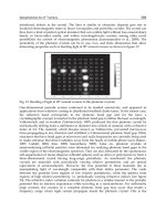
Fig. 24. SEM cross-section of PS micro-cavity with λ/2-wavelength thickness spacer for
centered wavelength of 650 nm (a) and PS size in the spacer layer (b).
The preparation of PS structures composed by several layers for DBR micro–cavity with
narrow band-pass width of 2 nm as a design by simulation is difficult in practice, because
the line-width of transmission of micro-cavity was strongly affected by homogeneity of the
layers. The anodization condition might drift as the sample thickness and refractive index of
stacks, and the solution composition changes with the depth because of limited exchange
through the pores, that caused the different of experimental results in comparison with
simulation one. In general, the band-pass width of 20 nm at the visible region obtained from
the PS micro-cavity based on electrochemical etching technique is good enable for
applications in the optical sensor, biosensors and/or micro-cavity lasers.
400 500 600 700 800
0
10
20
30
40
50
60
70
80
Reflectivity (%)
Wavelength (nm)
Fig. 25. Reflection spectrum of PS micro-cavity with transmission band of 650nm made by
spacer of λ/2- thickness sandwiched between 5-period DBR.
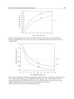
For a prevention of ageing process of PS layers we used thermal annealing process of PS
samples to obtain SRSO materials. The thermal annealing process used for SRSO has four
steps: i) first the PS samples were kept at 60
0
C for 60 min in air ambient to stabilize the PS
(a) (b)
Silicon–Rich Silicon Oxide Thin Films Fabricated by Electro-Chemical Method
51
structures; ii) the pre-oxidation of PS samples was performed at 300
0
C for different times
varying from 20 to 60 min in oxygen ambient; iii) slowly increasing temperature up to 900
0
C
and keeping samples for 5-10 min in oxygen ambient iv) keeping the samples in Nitrogen
atmosphere at temperature of 900-1000
0
C for 30 min and then the temperature was
decreased with very slow rate to room temperature. Table 5 presents the shift of
transmission band in the spectra of Fabry-Perot filters based on the as-prepared and
thermally annealed PS micro-cavity at 300
0
C and 900
0
C in oxygen ambient, respectively.
Samples Centered wavelength Line-width of Distinction
of transmission (nm) transmission (nm) ratio (%)
as-prepared sample 643.9 22.2 40
300
0
/40 min 565.6 22.6 34
300
0
/40 min + 900
0
C/5 min 472.5 19.2 25
Table 5. Shift of narrow transmission band in the spectra of Fabry-Perot PS filters (the
anodization condition was shown in table 4)
The 900
0
C oxidation decreases the centered wavelength of transmission by more than 170nm
and the reflective distinction ratio on 15%, while the line-width of transmission does not
change. This can be explained as follows: the centered wavelength of transmission
corresponds to the optical thickness of spacer layer that is the product of refractive index
and layer thickness. During the oxidization process at high temperature the layer thickness
and refractive index of spacer decreased, which causes the shift of transmission wavelength
and decrease of reflective distinction ratio of micro-cavity.
6. Conclusions
We have demonstrated the electrochemical method combined with thermal annealing for
making PS and SRSO layers. The advantages of electrochemical method compared with
others to fabricate PS and SRSO layers are: low-cost fabrication and experimental setup;
compatibility to silicon technology for optoelectronic devices; fast fabrication process and
easily varying refractive index over wide range.
We showed that the ageing of PS by natural oxidation is disturbing as well as it causes a
change of the emission wavelength of nc-Si, refractive index of PS layers by the change of Si
nano-particle sizes. The experimental results indicate that the intense and stable emission in
the blue zone of the PL spectra observed in the considered PS samples relates to defects in
silicon oxide layers. For prevention of natural oxidation of PS layers we used thermal
annealing to obtain SRSO layers, which have more stable optical properties in operations.
Also, the Er-doped SRSO multi-layers with good waveguide quality fabricated by using the
electrochemical method combined with thermal annealing are presented. The influence of
the parameters of the preparation process, such as the resistivity of Si-substrate, the HF
concentration, the drift current density, and the oxidation temperature, on the optical
properties of the Er-doped SRSO waveguides was studied and discussed in detail. The
luminescence emission of Er ions in the SRSO layers at 1540 nm was strongly increased in
comparison with that of Er-doped silica thin film. The evidence for energy transfer between
nc-Si and Er ions in Er-doped SRSO layer was obtained by changing the excitation
wavelength.
Optoelectronics - Materials and Techniques
52
Finally, we have demonstrated the electrochemical process for making interference filters
and DBR micro-cavity based on PS and SRSO multi-layers with periodical change of
refractive indices of the layer stacks. For the optimal parameters of interference filters and
micro-cavities based on PS and SRSO multi-layers, we use Transfer Matrix Method for
simulation of reflectivity and transmission of interference filters and DBR micro-cavity with
the data obtained from experiments. We successfully fabricated the interference filters and
DBR micro-cavity based on porous silicon multilayer which has the selectivity of
wavelength in a range from visible to infra-red range with the reflectivity of about 90% and
transmission line-width of 20nm. The spectral characteristics of those multi-layers such as
desired centered wavelength (λ
0
), the FWHM line-width of spectrum, reflectance and
transmission wavelength have been controlled. A good correspondence between simulation
and experimental results has been received. The imperfection of interfaces of layers created
by electrochemical etching was used to explain a deformation of reflective spectrum from
filters having few periods. The SRSO thin films with single and multi-layer structures
produced by electrochemical method have a big potential for applications in the active
waveguide, optical filter, chemical and biosensors, DBR micro-cavity lasers.
7. Acknowledgements
This work was supported in part by the National Program for Basic researches in Natural
Science of Vietnam (NAFOSTED) under contract No. 103.06.38.09. A part of the work was
done with the help of the National Key Laboratory in Electronic Materials and Devices,
Institute of Materials Science, Vietnam Academy of Science and Technology, Vietnam. The
author would like to thank Pham Duy Long for his help with Autolab equipment.
8. References
Amato, G., Rosenbauer, M. (1997). Absorption and photoluminescence in porous silicon, in
Amato et al. (ed.), Structure and Optical Properties of Porous Silicon Nanostructures,
Gorden and Breach Science Publishers, Amsterdam, 3-52
Anderson, M.A., Tinsley-Brown, A., Allcock, P., Perkins, E.A., Snow, P., Hollings, M., Smith,
R.G., Reeves, C., Squirrell, D.J., Nicklin, S., Cox, T.I. (2003), Sensitivity of the optical
properties of porous silicon layers to the refractive index of liquid in the pores,
Phys. Stat. Sol. (a) 197, 528-533
Barla, K., Herino, R., Bomchil, G. (1986). Stress in oxidized porous silicon layers, J. Appl.
Phys. 59, 439-441
Bettotti, P., Cazzanelli, M., Dal Negro, L., Danese, B., Gaburro, Z., Oton, C.J., Vijaya
Prakash, G., Pavesi, L. (2002). Silicon nanostructure for photonics, J. Phys.: Condens.
Matter. 14, 8253- 8281
Bui Huy, Pham Van Hoi, Phan Hong Khoi, Nguyen Thuy Van, Do Thuy Chi (2011). Porous
silicon as a promising material for photonics, Int. J.NanoTech. 8, 360-370
Bui Huy, Phi Hoa Binh, Bui Quang Diep, Phi Van Luong (2003). Effect of ageing on the
luminescence intensity and lifetime of porous silicon: role of recombination centers,
Physica E 17, 134-136
Bui Huy, Pham Van Hoi, Phi Hoa Binh, Tran Thi Kim Chi, Le Quang Huy, Nguyen Quang
Liem (2006). Effect of ageing on the statically and time-resolved photoluminescence
spectra of porous silicon, J. Phys. IV France 132, 321-324
Silicon–Rich Silicon Oxide Thin Films Fabricated by Electro-Chemical Method
53
Calcott, P.D.J., Nash, K.J., Canham, L.T., Kane, M.J., Brumhead, D. (1993) Spectroscopic
identification of the luminescence mechanism of highly porous silicon, J. Lumines.
57, 257-269
Canham, L.T. (1990). Si quantum wire arrays fabrication by electrochemical and chemical
dissolution of wafer, Appl. Phys. Lett.57, 1046-1048
De Stefano, L., Rendina, I., Moretti, L., Rossi, A.M. (2003), Optical sensing of flammable
substances using porous silicon microcavities, J. Mater. Sci. and Eng. B100, 271-274
Elhouichet, H., Oueslati, M. (2007). Rare earth ions in porous silicon: optical properties, J.
Phys. Stat.Sol. (a), 204, No.5, 1497-1501
Friolo, F., Franzo, G., Pacifici, D., Vinciguerra, V., Iacona, F., Irrena, A. (2001). Role of the
energy transfer in the optical properties of undoped and Er-doped interacting Si
nanocrystals, J. Appl. Phys. 89, 264-272
Frohnhoff, S., Berger, M.G., Thönissen, M., Dicker, C., Vescan, L., Munder, H., Lüth, H.
(1995). Formation techniques for porous silicon superlattices, Thin Solid Films 255,
59-62
Gao, T., Gao, J., Sailor, M.J. (2002), Tuning the response and stability of thin film
mesoporous silicon vapor sensors by surface modification, J. Langmuir 18, 9953-
9957
Gorelkinskii, Yu.V., Abdullin, Kh.A., Kalykova, G.K., Kikarin, S.M., Mukashev, B.N. (2008).
Stable ultraviolet photoluminescence of nanoporous silicon, J. Mater.Sci. & Eng.B
147, 258-261
Herino, R., Bomchil, G., Barla, K., Bertrant, C., Ginoux, J.L. (1987), Porosity and Pore size
distributions of Porous silicon layers, J. Electrochem. Soc. 134, 1994-2000
Huy. B., Cham T.T., Vinh H.X., Van D.K. and Hoi P.V. (2008). Erbium-doped silicon-rich
oxide waveguides fabricated by using an electro-chemical method, J. Korean Phys.
Soc.53, 1397-1400
Kanemitsu, Y., Uto, H., Masumoto, Y., Futagi, T., Mimura, H. (1993). Microstructure and
optical properties of free-standing porous silicon films: Size dependence of
absorption spectra in Si nanometer-sized crystallites, Phys. Rev. B 48, 2827-2830
Kimura, T., Yokoi, A., Horiguchi, H., Saito, R., Ikoma, T., Saito, A. (1994). Electrochemical
Er-doping of porous silicon and its room-temperature luminescence at 1.54 μm,
Appl. Phys. Lett. 65, 983-985
Kit, P.G., Polman, A. (2000). Exciton-erbium interactions in Si nanocrystal-doped SiO
2
, J.
Appl. Phys. 88, 1992 (7 page)
Kovalev, D., Averboukh, B., Benchorin, M., Koch, F., Efros, Al.L., Rosen, M. (1996). Optically
induced polarization anisotropy in porous silicon, Phys. Rev. Lett. 77, 2089-2092
Krüger, M., Hilbrich, S., Thönissen, M., Scheyen, D., Theiβ, W., Lüth, H. (1998). Suppression
of ageing effect in porous silicon interference filters, Opt. Comm. 146, 309-315
Lehmann, V., Gösele, U. (1991). Porous silicon formation – a quantum wire effect, Apll. Phys.
Lett. 58, 856-858
Loni, A., Canham, L.T., Berger, M.G., Arens-Fischer, R., Munder, H., Lüth, H., Arrand, H.F.,
Benson, T.M. (1996), Porous silicon multilayer optical waveguides, Thin Solid Films
276, 143-146
Mazzoleni, C., Pavesi, L. (1995). Application to optical components of dielectric porous
silicon multilayer, Appl. Phys. Lett. 67, 2983-2985
Optoelectronics - Materials and Techniques
54
Najar, A., Charrier, J., Ajlani, H., Lorrain, N., Elhouichet, H., Oueslati, M., Haji, L. (2006).
Optical properties of erbium-doped porous silicon waveguides, J. Lumines. 121, 245-
248
Saleh, B.E.A., Teich, M.C. (2007), Fundamentals of Photonics, 2nd Edition, Chapter 7, John
Wiley&Son, Inc., NewYork.
Shin, J. H., van d
’
Hoven, G. N., Polman, A. (1995). Origin of the 1.54 μm luminescence of
Erbium-implanted porous silicon, Appl. Phys.Lett. 66, 2379-2381
Smith, R.L., Collins, S.D. (1992). Porous silicon formation mechanism, J. Appl.Phys. 71(8), R1
(21 pages)
Valance, A. (1997). Theoretical model for early stages of porous silicon formation from n-
and p-type silicon substrates, Phys. Rev. B 55, 9706-9715
Vincent, G. (1994). Optical properties of porous silicon superlattices, Appl. Phys. Lett. 64,
2367 (3 page)
Volk, J., Balazs, J., Tóth, A.L., Bársony, I. (2004), Porous silicon multilayers for sensing by
tunable IR-transmission filtering, J. Sensors & Actuators B100, 163 -167
Weiss, S.M., Fauchet, P.M. (2003), Electrical tunable porous silicon active mirrors, Phys. Stat.
Sol (a) 2, 556-560
Wolkin, M.V., Jorne, J., Fauchet, P.M. (1999). Electronic states and luminescence in porous
silicon quantum-dots: the role of oxygen. Phys. Rev. Lett. 82,197-200
3
Silicon Oxide (SiO
x
, 0<x<2):
A Challenging Material for Optoelectronics
Nicolae Tomozeiu
R&D Department, Océ Technologies B.V.,
The Netherlands
1. Introduction
1.1 Why SiO
x
in optoelectronics
A complete integration of the silicon based optoelectronic devices was not possible, for
many decades, to be made because the silicon is an inefficient emitter of light. Being a
semiconductor with an indirect band-gap and having efficient free carrier absorption of the
radiation, the crystalline silicon was considered an inadequate material for light emitter
diodes (LED) and laser diodes to produce totally integrated optoelectronic devices. In the
last two decades, special attention has been paid to the light-emission properties of low-
dimensional silicon systems: porous silicon (Cullis & Canham, 1991; Wolkin et al., 1999),
super-lattices of Si/SiO
2
(Zu et al.,1995)
,
silicon nano-pillars (Nassiopoulos et al., 1996),
silicon nanocrystals embedded in SiO
2
(Wilson et al., 1993) or in Si
3
N
4
(Cho et al., 2005).
Both, the theoretical understanding of the physical mechanisms (quantum confinement of
excitons in a nano-scale crystalline structure) and the technological advance to manufacture
such structures have paved the path to produce a silicon based laser.
Pavesi at al (2000) have unambiguously observed modal and net optical gains in silicon
nanocrystals. They have compared the gain cross-section per silicon nano-crystal with that
the one obtained with A
3
B
5
(e.g. GaAs) quantum dots and it was found orders of magnitude
lower. However, owing to the much higher stacking density of silicon nanocrystals with
respect to direct band-gap A
3
B
5
quantum dots, similar values for the material gain are
observed. In this way, the route towards the realization of a silicon-based laser, and from
here, of a highly integrated silicon based optoelectronic chip, is open.
The silicon nano-crystals (Si-nc) embedded in various insulators matrix have been intensively
studied in the last decade. Either the photoluminescence (PL) properties of the material or the
emitted radiation from a LED/ diode laser structure was studied. A clear statement was made:
the peak position of PL blue-shifts with decreasing the size of Si-nc. The nano-crystals interface
with the matrix material has a great influence on the emission mechanism. It was reported that
due to silicon-oxygen double bonds, Si-nc in SiO
2
matrix has localized levels in the band gap
and emits light in the near-infrared range of 700–900 nm even when the size of Si-nc was
controlled to below 2 nm (Wolkin et al., 1999; Puzder et al., 2002).
In the last decades, silicon suboxides (hydrogenated and non-hydrogenated) have been
proposed as precursors for embedded silicon nano-crystals into silicon dioxide matrix. This
material is a potential candidate to be used in laser diodes fabrication based on silicon
technology. The need for such device was (and is) the main reason for theoretically (ab initio
Optoelectronics - Materials and Techniques
56
theories) and experimentally investigations of SiO
x
. This chapter dedicated to silicon
suboxide as a challenging material for silicon based optoelectronics, begins in section two
with a small (but comprehensive) discussion on the structural properties of this material.
The implications of the SiO
x
composition and its structural entities on the phonons’
vibrations are shown in the third section. Here are revealed the IR spectra of various
compositions of the SiO
x
thin films deposited by rf reactive sputtering and the fingerprints
related to various structural entities. The electronic density of states (DOS) for these
materials is the subject of the forth section. Here are defined the particularities of the
valence- and conduction band with special attention to the structural defects as silicon
dangling bonds (DB). Having defined the main ingredients to understand the optical and
electrical properties of the SiO
x
layers, these properties are discussed in the fifth and the
sixth section, respectively. The investigations and their results on as deposited SiO
x
materials are analyzed in this section. In the first part of this introduction it was mentioned
that the material for optoelectronics is the silicon nano-crystals embedded in SiO
2
. The
physical processes in order to obtain the silicon nano-particles from SiO
x
thin films are
presented in section seven. The phase separation realized with post-deposition treatments as
thermal annealing at high temperature, or ion bombardment or irradiation with UV photons
is extensively discussed. This section ends with a brief review of the possible applications of
the Si-nc embedded into a dielectric matrix as optoelectronic devices. Of course the main
part is dedicated to the silicon-based light emitters.
2. The structure of SiO
x
(0<x<2)
2.1 Introductive notions
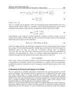
The structure of the silicon oxide, as the structure of other silicon-based alloys, is build-up
from tetrahedral entities centered on a silicon atom. The four corners of the tetrahedral
structure could be either silicon or oxygen atoms. Theoretically, this structural edifice
appears as the result of the “chemistry” between four-folded silicon atoms and two-folded
oxygen atoms, developed under specific physical conditions. It is unanimously accepted
that an oxygen atom is bonded by two silicon atoms and never with another oxygen atom.
The length of the Si-O bond is 1.62 Å while the Si-Si bond is 2.35 Å. The dihedral
anglebetween two Si-Si bonds (tetrahedron angle) is 109.5
0
and the angle formed by the Si-O
bonds in the Si-O-Si bridge is 144
0
. These data are the results of dynamic molecular
computation (Carrier et al., 2002) considering the structure completely relaxed. In reality,
the structure of the SiO
x
thin films deposited by PVD or CVD techniques is more
complicated. Both the bond length and the dihedral angle vary. Moreover, the picture of the
structural design is complicated because the Si-O bond is considered partially ionic and
partially covalent (Gibbs et al., 1998).
2.2 SiO
x
structure: theoretical assumptions
In order to obtain an elementary image of the SiO
x
structure, we use a simple model. It is
important to evaluate the main elements that define the material structure: the energy
involved in keeping together the atoms within a specific structure and the number of each
atom species from a defined alloy. The Si–Si and Si–O bonds are characterized by
dissociation energy of 3.29 eV/bond and 8.26 eV/bond, respectively (Weast, 1968). The
particles’ density in crystalline silicon (c-Si) is 5·10
28
m
-3
while for crystalline quartz (c-SiO
2
)
is 6.72·10
28
m
-3
. Interpolating, it can be found for SiO
x
:
Silicon Oxide (SiO
x
, 0<x<2): A Challenging Material for Optoelectronics
57
x
at 28 27
SiO
N 5 10 8.55 10 x=⋅ + ⋅ ⋅ (m
-3
), (1)
where x=O/Si.
The silicon atoms’ density is:
x
at
Si SiO
1
NN
1x
=⋅
+
(2a)
and the oxygen atoms’ density is:
x
at
OSiO
x
NN
1x
=⋅
+
(2b)
Taking into account the fact that the silicon atom is four-coordinated and the oxygen is two-
coordinated, the number of bonds can be easily calculated:
• O atoms are involved in Si–O–Si bridges
1
, which means two Si-O bonds: n(Si–O–Si) =
2·n (Si–O) = N
O
(one oxygen atom contributes to two Si-O bonds);
• Si atoms will contribute to Si–Si and Si–O–Si bonds: n(Si–Si, Si–O–Si)=(4/2)·N
Si
, (one
silicon atom is shared by 4 Si-Si and/or Si-O bonds and it must be considered only
once);
This means that for Si – Si bonds it is easy to write: n(Si–Si)= n(Si–Si, Si–O–Si) – n(Si–O–Si),
where n(A -B) is the number of bonds between atom specie A and atom specie B from an AB
alloy, while N
y
, with y=Si, O is the number of specie “y” atoms.
Having the number of bonds and the energy per bond, the energy involved in a SiO
x
material can be estimated. This represents practically the necessary energy to break all
bonds between the atoms that form a structural edifice. Following the calculations presented
above, the density of Si–Si and Si–O bonds versus silicon suboxide composition (x
parameter from SiO
x
) is shown in figure 1a. Also, the values of the SiO
x
density energy (in J/
m
3
) calculated for x ranging between 0 and 2 are displayed in figure 1b. The latter is an
important parameter for experiments considering the structural changes of an already
deposited (grown) SiO
x
material.
0.0 0.5 1.0 1.5 2.0
10
28
10
29
n
Si-Si
n
Si-O
Nr. of bonds / m
3
x (from SiO
x
)
(a)
0.0 0.5 1.0 1.5 2.0
4.0x10
10
6.0x10
10
8.0x10
10
1.0x10
11
1.2x10
11
Energy (bonds' energy) (J/m
3
)
x (from SiO
x
)
(b)
Fig. 1. (a) The calculated values of the Si-Si and Si-O bonds density as a function of x; (b) the
dissociation energy per volume unit versus x parameter.
1
The number of O-O bonds is considered as being equal to zero.
Optoelectronics - Materials and Techniques
58
The interpretation of the data presented in figure 1b, is simple: for a sample with certain x
value, if the corresponding value of the dissociation energy is instantaneously delivered, we
can consider that for an extremely short time, the bonds are broken and the atoms can “look
for” configurations thermodynamically more stable. With short laser pulses, such kind of
experiments can be undertaken and structural changes of the material can be studied.
2.3 The main SiO
x
structural entities
Varying the number of oxygen atoms bonded to a silicon atom considered as the center of
the tetrahedral structure, five entities can be defined. In a simple representation they are
shown in figure 2. For a perfect symmetric structure (the second order neighboring atoms
included), the Si–Si distance is 1.45 times the Si–O length. The nature of the Si–O bond
makes the pictures shown in figure 2 more complicated. The electrical charge transferred to
the oxygen neighbor charges positively the silicon atom. This means that a four-coordinated
silicon can be noted as Si
n+
where n is the number of oxygen atoms as the nearest neighbors.
The length of a Si–Si or Si–O bond, as well as the angle between two adjacent bonds, is
influenced by the n+ value and the spatial distribution of those n oxygen atoms around the
central silicon atom. Of course the 4-n silicon atoms are also Si
m+
like positions and they will
influence the length of the Si
n+
- Si
m+
bond. Using first-principles calculations on Si/SiO
2
super-lattices, P. Carrier and his colleagues (Carrier et. al., 2001) have defined the interfaces
as being formed by all Si
1+
, Si
2+
and Si
3+
entities. The super-lattice structure has been
considered within a so-called
fully-relaxed model. The main outcome of these calculations is
that the bond-lengths of partially oxidized Si atoms are modified when compared with their
counterparts from Si and SiO
2
lattice. As examples we mention: within a Si
1+
structure the
Si
1+
– Si
m+
bond is 2.39 Å for m=2 and 2.30 Å when m=0. The Si
n+
- O has a length of 1.65Å
when n=1 and 1.61 Å for n=3. All these have influences on the structural properties of the
material and from here on the density of states assigned to the phonons and electrons. The
influence on physical properties (electrical, optical and mechanical) of the material
deposited in thin films will be discussed in the next sections.
O
Si
2.35Å
Si
1
.62Å
Fig. 2. The five structural entities defined as Si
n+
in SiO
x
alloys. The structures are build-up
around a central Si atom from n oxygen atoms (the filled circles) and 4-n silicon atoms
(empty circles)
It should be noted that the differences in both the bond length and the dihedral angle of two
adjacent bonds determine, for each structural entity, small electrical dipole with great
impact on properties as electrical conductivity and dielectric relaxation. A contribution of
the polarization field on the local electrical field will determine hysteresis – like effects, that
could be used in some applications.
The multitude of possible connexions between various structural entities defines on
macroscopic scale a SiO
x
structure full of mechanical tensions which, speaking from a
Silicon Oxide (SiO
x
, 0<x<2): A Challenging Material for Optoelectronics
59
thermodynamic perspective, provides an unstable character to the material. It is easy to see
that a material formed from Si
0+
or Si
4+
structures without defects (e.g. dangling bonds) is
thermodynamically stable.
3. The phonons’ vibrations and SiO
x
structure
3.1 Phonons’ and molecular vibrations
Within the so-called Born – Oppenheimer adiabatic approximation, the general theory of
solid state physics shows that the movement of the light particles-component of atoms
(electrons) can be neglected or considered as a perturbation for the movement of the heavy
parts of the atom (ions). In these conditions, for a crystalline material, the Schrödinger
equation assigned to the system of heavy particles is:
{
}
(
)
{
}
(
)
ˆ
z
HR ER
αα
Ψ=Ψ
G
G
(3)
where the Hamiltonian
ˆ
z
H is a sum of three terms:
i.
the first one describes the kinetic energy:
2
2
P
M
α
α
α
⎛⎞
⎜⎟
⎜⎟
⎝⎠
∑
, with α the number of particles,
M
α
and P
α
- the mass and the momentum of the ion;
ii.
the second one :
,( )
1
ˆ
2
V
α
β
αβα β
≠
∑
is the potential energy due to the interaction between
ions;
iii.
and the third one defined as
{
}
(
)
ˆ
e
ER
α
G
represents the electrostatic interaction between
ions and electrons.
The equations (3) have been solved considering that the lattice vibrations involve small
displacement from the equilibrium position of the ion: 0.1 Å and smaller. Under the so-
called harmonic approximation, the problem is seen as a system of quantum oscillators with
the solution:
• the eigenvector Ψ was found as
α
α
ψ
Ψ=
∏
(4)
with
()
exp
()
k
ikR
uR
V
α
αα
α
ψ
=⋅
G
G
G
G
given by the Bloch functions.
• the eigen-values for energy:
1
2
EE hN
ααα
αα
ν
⎛⎞
== ⋅+
⎜⎟
⎝⎠
∑∑
(5)
The relation (5) shows that
h
α
ν
is a quantum of energy assigned to the lattice oscillation. It
represents the energy of a phonon – quasi-particle that describes the collective movement of
the lattice constituents. The phonons are characterized by energy and momentum (impulse)
Optoelectronics - Materials and Techniques
60
as long as the lattice and the collective movement of the atoms (ions) exists. Only under
these conditions, the phonon can be understood as a particle that can interact with other
particles (e.g. electrons, photons).
Let us consider a molecule formed from different atoms where the bond lengths and the
bond angles represent the average positions around which atoms vibrate. At temperatures
above absolute zero, all the atoms in molecules are in continuous vibration with respect to
each other. If the molecule is consisting of N atoms, it has a total of 3N degrees of freedom.
For nonlinear molecules, 3 degrees of freedom describe the translation motion of entire
molecule in mutually perpendicular directions (the X, Y and Z axes) and other 3 degrees
correspond to rotation of the entire molecule around these axes. For a linear molecule, 2
degrees are rotational and 3 are translational. The remaining 3n-6 degrees of freedom, for
nonlinear molecules, respectively 3n-5 degrees for linear molecules are fundamental
vibrations, also known as normal modes of vibration.
Considering the adiabatic approximation and harmonic displacements of the atoms from
their equilibrium positions, for each vibrational mode, q, all the atoms vibrate at a certain
characteristic frequency,
ν
q
called fundamental frequency. In this situation, for any mode the
vibration energy states, E
q
ν
, can be described by:
harm
1
Eh
2
q
n
ν
ν
⎛⎞
=+
⎜⎟
⎝⎠
(6)
where h is Planck’s constant, n
q
is the vibrational quantum number of the q-th mode (n
q
=0,
1, 2, …). The ground state energy (that corresponds to n
q
= 0) is h
ν
q
/2 and each excited state,
defined by the vibrational quantum number has an energy defined by the Rel. (6). The
energy difference for transitions between two adjacent states is constant and equals h
ν
q
.
The theoretical model of the harmonic displacement of the atoms helps to easily describe the
atoms movement. In reality, the structural edifice of the molecule supposes atoms that
belong to intra-molecule bonds or to inter-molecules bonds. This means that the character of
harmonic oscillator disappears and a molecule is in fact an anharmonic oscillator.
Introducing an anharmonicity parameter
γ
q
for each vibrational mode, the phonon energy
can be expressed as:
2
1
2
harm
qq qqq
EE h n
νν
νγ
⎛⎞
=+ +
⎜⎟
⎝⎠
(7)
where γ
q
is dimensionless.
How the length of the bond (the interatomic distance) influences the phonon energy?
Considering a di-atomic molecule, its potential energy as a function of the distance between
the atoms within an anharmonic oscillation is suggestively shown in figure 3. The minimum
in the potential energy is reached when the distance between the two atoms equals the
“bond length”. As the inter-atomic distance increases, the potential energy reaches a
maximum, which defines the bond dissociation energy.
An interesting observation is that the energy levels of the oscillator which represents the
diatomic molecule are quantified (they have discrete values) and they become closer with
increasing the interatomic distance. This means that the needed energy to excite the phonon
on the nearest energy state, hν
q
, is smaller when the distance between the atoms increases.
Silicon Oxide (SiO
x
, 0<x<2): A Challenging Material for Optoelectronics
61
-2
-1.5
-1
-0.5
0
0.5
1
1.5
0.8 1 1.2 1.4 1.6 1.8 2 2.2 2.4
interatomic distance
energy
0
1
2
3
bond length
h
ν
dissociation
energy
Fig. 3. The potential energy for a di-atomic molecule versus the interatomic distance, within
the anharmonic oscillation model.
How the mass of the two atoms influences the phonon frequency? To answer this question, let’s
consider the simplest oscillator (a mechanical spring connecting two masses) and apply the
classical Hooke’s law. If m
1
and m
2
are the mass values for the two atoms, the frequency
oscillation is:
1
2
k
ν
π
μ
=⋅ (8)
with the reduced mass,
μ
, given by
12
12
mm
mm
μ
=
+
. The parameter k is called the elastic force
constant of the bond and it defines the bond strength.
In most books of the IR spectroscopy the oscillation frequency is given in wave-number unit
that is the inverse of the wavelength. In this condition the Rel. (8) becomes
11
2
k
c
ν
λπ
μ
== ⋅
(cm
-1
) (8’)
with c the speed of light, 3·10
10
cm/s. Therefore, for the heavier atoms the vibration
frequency is smaller. However the strength of the bond is also defining the vibrational
frequency. In other words, the nature of the bond is important. We can conclude that the
phonon spectrum is specific to each type of molecule and it could be utilized in
identification of the atomic species.
We note that, within a multi-atomic molecule, the motion of two atoms cannot be isolated
from the motion of the rest of the atoms in the molecule. Also, in such a molecule, two
oscillating bonds can share a common atom. When this happens, the vibrations of the two
bonds are coupled.
3.2 IR active vibrations - a theoretical approach
IR spectroscopy is one of the most utilized techniques in analyzing the compositional and
structural properties of a molecular compound. When a radiation of IR optical range, with
Optoelectronics - Materials and Techniques
62
energy hν, is sent on a molecular system whose vibration frequency is ν, that radiation is
absorbed, if the molecule has electrical dipole.
As a result of the interaction between the electrical field of the IR electromagnetic wave and
the molecular dipole, the molecule will make a transition, in energy, between the states “i”
and “j”. The transition moment ℑ is defined by:
*
i
j
ψμψdτℑ=
∫
(9)
where ψ and ψ
*
are the eigen-function and its complex conjugate; dτ is the integration over
all space. In the relation (9) μ is the dielectric dipole moment defined as:
μ qr=⋅ (10)
with q the charge of the dipole and r the distance between the charges.
Taking into account the vibrational motion of the atoms, the dielectric dipole changes,
because the distance r changes:
2
2
0e e
2
0
0
μ 1 μ
μμ (r r ) (r r )
r2
r
⎛⎞
∂∂
⎛⎞
=+−⋅ +⋅− ⋅ +
⎜⎟
⎜⎟
⎜⎟
∂
∂
⎝⎠
⎝⎠
In this situation the transition moment becomes:
*
i0 e j
0
μ
ψμ (r r ) ψ dτ
r
⎡⎤
∂
⎛⎞
ℑ= + − ⋅ ⋅
⎢⎥
⎜⎟
∂
⎝⎠
⎢⎥
⎣⎦
∫
(11)
When μ
0
is a constant, because of the orthogonality of the eigen-functions, (
*
ij
ψψdτ 0=
∫
),
the relation (11) remains:
*
ie j
0
μ
ψ (r r ) ψ dτ
r
⎡⎤
∂
⎛⎞
ℑ= − ⋅ ⋅
⎢⎥
⎜⎟
∂
⎝⎠
⎢⎥
⎣⎦
∫
(12)
The transition probability is defined as
2
ℑ , and it scales the radiation absorption. With
other words, the intensity of the IR absorption peak is proportional to the square of ℑ and
μ
r
∂
⎛⎞
⎜⎟
∂
⎝⎠
. We can say that the
molecules with
μ
0
r
∂
⎛⎞
=
⎜⎟
∂
⎝⎠
are IR inactive because the absorption of
the radiation is zero. We note that molecule with small dipole moment μ may have large
μ
r
∂
⎛⎞
⎜⎟
∂
⎝⎠
and vice-versa. In both situations, according to Rel. (12), absorbing bands will appear
in the IR spectrum.
Therefore, we can conclude that among the fundamental vibrations, those that produce a
change in the dipole moment may result in an IR activity. Certain vibrations
give
polarizability changes and they may give Raman activity
. Some vibrations can be both IR- and
Raman-active.
Silicon Oxide (SiO
x
, 0<x<2): A Challenging Material for Optoelectronics
63
3.3 The IR fingerprints of the SiO
x
structural entities
Does the SiO
x
structure have an electrical dipole to interact with the incident IR radiation
and to release an IR absorption spectrum?
Considering the structural entities presented in figure 2, all entities that contain at least one
oxygen atom have such an electrical dipole. The tetrahedral structure build up around a
silicon atom by its four neighbors will have a certain asymmetry concerning the "gravity
center" of the positive charge vis-à-vis of that the one of the negative charge. By molecular
vibration a dipole is generated and, according to the theoretical explanation given in the
previous section, energy of the IR electromagnetic field will be absorbed.
Calculations based on theoretical models (simpler or more sophisticated, modern) have
produced the local density of vibrational states (LDOVS) for Si and O atoms (Lucovski and
Pollard, 1963, Knights et al., 1980, Pai et al., 1986). The IR absorption spectrum specific to a
SiO
2
structure was calculated taking into account these LDOVS’ and as it can be seen in
figure 4 (after P.G. Pai et al., 1986) there are three vibrational bands which correspond to
rocking, bending and stretching motions of the oxygen atoms. As a first observation, the
dominant calculated peak in the IR absorption spectrum of SiO
2
is associated with stretching
motion of the oxygen atoms. The peak position and the shape of the peak absorption are
greatly affected by the mixing of Si and O atoms.
Fig. 4. Local density of vibrational states (LDOVS) for oxygen and silicon and, calculated IR
response for silicon dioxide.
Reprinted with permission from Pai et al., 1986; copyright 1986,
American Vacuum Society.
According to the model proposed by Pai and his colleagues (Pai et al., 1986), this peak is an
interesting example of coupled oscillations: the motion of the oxygen atom and that of the
neighboring silicon atoms. The low frequency part of the spectrum peak is “imposed” by the
silicon atoms’ vibration (the motion of the oxygen atom is in phase). The high frequency
edge of the same peak is dominated by oxygen; there is a little associated silicon motion,
which is out of phase motion compared with the movement of the oxygen atoms. A broad
shoulder centered at about 1150cm
-1
generally gives this part of the peak.
Optoelectronics - Materials and Techniques
64
The IR vibrations of a Si–O–Si entity belonging to the SiO
x
structure are briefly presented as
following:
•
a bond-stretching vibration, ν
s
, in which the O displacement is in a direction parallel to
the line joining its neighboring silicon (in a-Si matrix, the peak absorption is placed at
940cm
-1
and in thermally growth a-SiO
2
is at 1073cm
-1
);
•
bond-bending vibration, ν
B
, in which the O atom motion is along the bisector direction
of the Si-O-Si bond angle (ν
B
=780cm
-1
);
•
out of plane rocking motion, ν
R
, with ν
R
=450cm
-1
.
The majority of the published papers reveal the particularities of the stretching vibration peak.
The oxygen atom is bonded to two adjacent silicon atoms by Si–O bonds. Considering the
diatomic model described in the previous section, the movement of the oxygen atom is the
result of the coupling of the two Si–O vibrations. The strength of the bond and the vibration
frequency are dependent not only on the Si and O atoms partners in the bond, but also on the
other neighbors of the silicon atom. Schematically, the Si–O–Si bridge is shown in figure 5.
Si
O
Si, O
Fig. 5. A sketch of the Si–O–Si structural bridge with the other 6 atoms neighboring the two
silicon atoms, which can be either oxygen atoms or silicon.
A measured IR spectrum of a SiO
x
thin film deposited by reactive rf sputtering is shown in
figure 6. The thickness of the layer was determined as being d=620nm and the composition
corresponds to x=0.73. The rocking, bending and stretching modes of Si-O-Si are identified.
500 1000 1500 2000 2500 3000 3500 4000
0.00
0.05
0.10
0.15
0.20
0.25
0.30
0.35
Absorbance (a.u.)
Wavenumber (cm
-1
)
x=0.73
rocking
bending
stretching mode
Fig. 6. The IR spectrum of SiO
x
layer with x=0.73.
The peak position and the shape of the absorption peak assigned to the stretching vibration
mode depend on the composition. This is well revealed in figure 7 where the normalized
spectra are shown for SiO
x
samples with x between 0.1 and 2. Increasing the oxygen content,
the main peak position shifts towards larger wavenumber values, while its width becomes
smaller. For larger x values, (x>1.2), a shoulder appears on the 1150 cm
-1
, which becomes
more and more pronounced when the oxygen content increases. For x=2 this shoulder is a
characteristic feature for the SiO
2
structural entities.
Silicon Oxide (SiO
x
, 0<x<2): A Challenging Material for Optoelectronics
65
800 900 1000 1100 1200 1300 1400
0.0
0.2
0.4
0.6
0.8
1.0
x=0.1
0.25
0.45
0.65
0.85
1.2
1.44
1.82
SiO
2
th
Absorption coefficient (norm.)
Wavenumber (cm
-1
)
Fig. 7. The position and the shape of the absorption peak assigned to the stretching vibration
mode of the Si–O–Si bridge are dependent on the oxygen content.
The shift in the peak position could be used to scale the oxygen content. This is applied when
the samples have been deposited with the same technique, with well defined deposition
conditions. A calibration curve between the oxygen content previously determined via other
techniques (Rutherford back-scattering, or x-ray photoelectron spectroscopy, etc) and the IR
peak position is needed. It must be mentioned that, although this method to determine the
layer composition is used in many labs, the peak position is dramatically influenced by the
deposition conditions (Tomozeiu, 2006). There is another model to determine the oxygen
concentration from IR absorption measurements using the integrated absorption of the
stretching mode peak. Also here, it is necessary to calibrate the method. This means that for
some samples, the x parameter must be determined via other methods. The IR spectroscopy is
set as a secondary standard in measuring the oxygen content.
The method was proposed by Zacharias and his colleagues to determine the concentrations
of hydrogen and oxygen in a-Si:O:H thin films (Zacharias et al., 1994). It is based on the aria
of the IR absorption peak related to that atomic species and the connection with the
concentration is:
()
()
() ()
peak i
ci Ai d
ν
αν
ν
ν
=
∫
(13)
where c(i) is the concentration of element i (H or O),
α
(
ν
) is the absorption coefficient in the
peak region centered on
ν
peak
and A(i) is the calibration factor. Writing this formula for
SiO
x
, the oxygen concentration is: c(O)=A(O)*I(1080-960), where I(1080-960) is the integrated
absorption between
ν
=960 cm
-1
and
ν
=1080 cm
-1
.
For the spectra presented in figure 7 the calculated values of the integrated IR absorption are
shown in figure 8. A good linearity between the integrated absorption and the x values is
found for x<1.3. For samples with oxygen content higher than the value corresponding to
this point, there is a rapid increase of the integrated IR absorption. In other words, at x=1.3
there is a kink point (Tomozeiu et al., 2003) in the plot shown in figure 8. This was evaluated
as a signal that the SiO
x
structure changes from a random distribution of the Si–O bonds in
Optoelectronics - Materials and Techniques
66
the material bulk (RBM model) to a random mixing model (RMM) which describes the
material in terms of domains of fully oxidized silicon (SiO
2
) and low-oxygen silicon. Similar
results have been reported by F. Stolz and his colleagues (Stolz et al., 1993) on SiO
x
samples
prepared under other conditions than those investigated in the figure 7. For the data
presented in figure 8, the relation (13), in terms of x parameter, becomes:
()
4
x 5.49·10 ·I 1080 960 ,with x 1.3
−
=−< (13')
0.0 0.5 1.0 1.5 2.0
0.0
2.0x10
3
4.0x10
3
6.0x10
3
8.0x10
3
1.0x10
4
Integrated absorption
x
b)
Fig. 8. The integrated IR absorption of the stretching mode near 1000 cm
–1
versus the SiO
x
oxygen content. A kink point is outstanding near x=1.3
3.4 The material structure reflected in the IR absorption spectrum
Is the first part of the plot from figure 8 describing the SiO
x
structure based on a random bonding
model (RBM)?
The answer is based on a simpler theoretical model proposed by A Morrimoto and his
colleagues (Morimoto et al., 1987). They assumed a random distribution of the
Si-O-Si bonds
and they calculated the probability that “
n” oxygen atoms will neighbor a Si-O-Si bridge.
The probability to have “
n“ O-atoms and “6-n“ Si-atoms around the Si-O-Si bridge (see the
figure 6) is:
6
6
() ( ) ( ) 0 6
nnn
n
Px CPSi PO n
−
==÷
(14)
where
6
n
C gives the number of arrangements in which n sites are chosen from the total of 6
sites,
P(Si) and P(O) being the presence probability of Si and O, respectively.
Considering the number of
Si-Si bonds and the number of Si–O bindings as a function of
the oxygen content, (see section 2.2) the
P(Si) and P(O) probabilities are easy to calculate:
()
() 1
(, )2
nSi Si x
PSi
nSi Si Si O Si
−
==−
−−−
(15a)
and respectively:
()
()
(, )2
nSi O Si x
PO
nSi Si Si O Si
−−
==
−−−
. (15b)
Silicon Oxide (SiO
x
, 0<x<2): A Challenging Material for Optoelectronics
67
In this way, the probability to have the richest in silicon SiO
x
is given by Rel. (14) with n=0:
6
0
() 1
2
x
Px
⎛⎞
=−
⎜⎟
⎝⎠
and the probability to have the richest in oxygen SiO
x
is obtained for n=6:
6
6
()
2
x
Px
⎛⎞
=
⎜⎟
⎝⎠
. The probability to have Si–O–Si entities with “n” oxygen atoms around the
two silicon atoms, is naturally depending on the x value. For a SiO
x
structured as the RBM
predicts, the P
n
(x) is shown in figure 9.
0.0 0.5 1.0 1.5 2.0 2.5
0.0
0.1
0.2
0.3
0.4
0.5
0.6
Oo
O1
O2
O3
O4
O5
O6
P
n
(x) (a.u.)
x (SiO
x
)
Fig. 9. The calculated probabilities to have n O-atoms bonded by Si–O-Si.
With this plot, a rough estimation of the number of the oxygen atoms and how they are
bounded can be made for materials with known x parameter values. Such kind of maps are
shown in figure 10 for different x values of SiO
x
samples deposited via reactive sputtering.
We mention that this is a theoretical estimation within the RBM approximation.
0.0
0.2
0.4
0.6
0.8
P
n
(a.u.)
x=0.1
0.0
0.1
0.2
0.3
P
n
(a.u.)
O0
O1
O2
O3
O4
O5
O6
x=0.8
Fig. 10. The maps of the oxygen bounding probability on Si-O-Si structural bridge.
How much this model represents reality? This is a very important question for the applications
of the SiO
x
material and the answer will be found in the section 7.
Optoelectronics - Materials and Techniques
68
4. Electronic density of states (DOS) in SiO
x
4.1 Introductive notions about DOS of amorphous semiconductors
In crystalline semiconductors the periodic variations of the lattice potential give rise to
parabolic edges in k
G
-space for the electronic energy bands (Ashcroft and Mermin, 1988).
The conduction band is separated, in energy scale, from the valence band by the so-called
“band - gap”. In amorphous semiconductors there is no periodicity of the lattice. Both, the
bond length and the angle between two adjacent bonds vary with small amounts around
what the crystalline counterparts reveal. Considering the example of amorphous silicon, the
nearest neighbors (the first coordination sphere) are the same as for the crystalline silicon,
but a difference appears when we speak of near neighboring (e.g. the second coordination
sphere) where deviations of about ± 5
o
versus the crystallization direction appear. This gives
rise to the existence of tails attached to valence- and conduction- band that penetrate into the
band-gap. They are formed from localized states assigned to the carrier (electron).
Generally, it is assumed that the density of states in the tail decreases exponentially into the
gap.
Very often it happens that one bond is missing and the atom is sub-coordinated. Defects
represented in amorphous semiconductors by “coordination defects”, such as dangling
bonds,(DB), give rise to electronic states around midgap. Dangling bonds show an
amphoteric behavior, which means that a dangling bond can have three different charge
states: positively charged when unoccupied, neutral when singly occupied by electron and
negatively charged when doubly occupied. Such a defect is represented by two electronic
states. There are several approaches to model the distribution of defect states within the gap
of amorphous material. A standard model for the defect-state distribution assumes two
symmetrical Gaussian distributions separated by the so-called correlation energy (Street,
1991) (see figure 11).
Normally, such a defect has one unbounded electron and electrically the defect is neutral,
D
0
. But according to the Pauli’s rule, on the same energy level, another electron can be
accommodated (with unparallel spin) and the defect will become negatively charged, D
-
.
The energy level of D
-
, in comparison with D
0
will be raised due to electron-electron
interaction. The existence of D
-
defects implies the existence of positively charged defects,
D
+
, - dangling bonds where the electron is missing. The energy states assigned to DB are
localized and they form narrow bands near the mid-gap. The Fermi level is pinned between
them. Due to their electronic states placed deep into the band-gap, around Fermi level, the
defects control the optical and electrical properties of the amorphous material.
It is unanimously agreed that the energy bands (valence- and conduction-band) are formed
in amorphous semiconductors from extended states (their contribution to the transport
phenomena is similar to the homologous states in crystalline materials) and localized states
that form the tail. The delimitation between these two types of states is made by the mobility
edge levels; this name derives from the fact that the electron mobility is higher when
extended states are involved than the mobility of localized electrons (4 to 6 order of
magnitude). It is important to mention that the mobility edges in disordered materials play
the same role as the energy band edges in crystalline counterparts.
Structural disorder (deviations in bond length and bond angle) is represented in the density
of states distribution by localized states in the bands’ tails. Figure 11 shows the
Silicon Oxide (SiO
x
, 0<x<2): A Challenging Material for Optoelectronics
69
representation for density of electron states, N(E), as a function of energy, E, according to
the Mott and Davis model (Mott and Davis, 1979). The mobility edges of both the
conduction- and valence-band are depicted by E
C
and E
V
respectively. The tails of these
bands are considered as exponentially decaying into the band gap. In the case of bi- or
multi-component amorphous alloy local variations in stoichiometry (composition) may
appear. This means that the mobility edges will have a “sophisticated” spatial distribution.
D
-
D
+
Extended states
E
V
E
C
Localised states
E
N(E)
Fig. 11. Mott-Davis model for density of states (DOS) in disordered materials.
The DB density in amorphous materials depends on the quality of the material and on the
technology used for layer preparation. Typical values for sputtered a-Si are 10
19
spin/cm
3
while in SiO
x
could reach 10
22
spin/cm
3
. Thermal treatment (annealing) will help relax the
lattice and therefore variations in DB’s have been observed. Adding hydrogen during layer
deposition, the DB’s density will drastically decrease. The Si-H bonding energy lies deep in
the valence band (VB). Therefore, defects from mid-gap are removed through
hydrogenation.
4.2 Particularities of SiO
x
density of states
In the last decades, silicon suboxides have been theoretically (ab initio theories) and
experimentally investigated to better understand their electronic density of states (DOS). It
is well known that this parameter defines both the optical and the electrical properties of the
material. According to the random bonding model of the SiO
x
structure, clusters of Si
n
O
m
have been theoretically investigated at the quantum-mechanic level (Zhang et al., 2001a) and
it was found that:
•
energetically the most favorable small silicon-oxide clusters have O atomic ratios at
around 0.6;
•
remarkably high reactivity at the Si atoms exists in silicon suboxide Si
n
O
m
clusters with
2n>m.
The total density of states (TDOS) was theoretically calculated (Zhang et al., 2001b) and
projected onto the constituent atoms to deduce the contribution of the individual atoms to
the total electronic structures. Such a treatment was used to find the atoms in which the
Optoelectronics - Materials and Techniques
70
highest occupied molecular orbital – HOMO (to be assigned to the valence band edge from
crystalline semiconductors) and the lowest unoccupied molecular orbital – LUMO (similar
to the conduction band edge) reside. The difference LUMO-HOMO is an indication of the
material band-gap. The closest molecular orbital to the gap contains a significant
contribution from the Si and O atoms, as HOMO
Si
, HOMO
O
, LUMO
Si
, and LUMO
O
,
respectively. In figure 12 are shown the results of the calculations as a function of the
relative oxygen content into the layer. Zhang and his colleagues (Zhang et al., 2001a) have
used fourth-order polynomials fit, and in figure 12 are shown LUMO
Si
(upper) and HOMO
Si
(lower) with solid curves, while dashed curves represent LUMO
O
(upper) and HOMO
O
(lower). Therefore, considering a defect-free SiO
x
material, its band gap is determined by the
orbital of the atomic silicon for silicon-rich material and by the orbital of atomic oxygen for
silicon-poor materials. Increasing the oxygen content, the LUMO position remains at about
the same energy position, while the HOMO decreases.
Taking into account the localized states induced by dangling bonds in the region of mobility
band gap, the energy distribution of the density of states, can be penciled (Singh et al., 1992;
van Hapert, 2002) as in figure 13. This model is inspired by the data published till 2002 and
it is successfully utilized to understand the physical properties of SiO
x
thin films. As main
conclusions we point out:
•
the conduction band is formed by Si-Si and/or Si/O antibonding states;
•
the valence band is formed by Si-Si bonding states for SiO
x
with x<1.3 and by Si-O
bonding states for SiO
x
with x>1.3;
•
the silicon dangling bonds (DB) states form a band of localized electronic states at 0.7
eV below the conduction band edge.
Fig. 12. Computed LUMO
Si
(×), LUMO
O
(Δ), HOMO
Si
(+) and HOMO
O
(◊) of Si
n
O
m
clusters.
Reprinted figure with permission from Zhang et al., 2001a
2
. Copyright (2001) by American
Physical Society.
2
Zhang, R. Q.; Chu, T. S.; Cheung, H. F.; Wang, N. & Lee, S. T. Phys. Rev. B64, pp. 113304 - 113308
(2001)
Silicon Oxide (SiO
x
, 0<x<2): A Challenging Material for Optoelectronics
71
DOS
energy, E
E
C
=LUMO
E
V
= HOMO
Mobility
band-gap
Antibonding states
Bonding states
DB states => VRH
conduction mechanism
DOS
energy, E
E
C
=LUMO
E
V
= HOMO
Mobility
band-gap
Antibonding states
Bonding states
DB states => VRH
conduction mechanism
Fig. 13. Model for SiO
x
density of states distribution.
4.3 The nature of the paramagnetic defects in SiO
x
In the section 4.1 it was shown that the structural defects defined by dangling bonds can be
electrically neutral and positively or negatively charged. Defects’ type and their density
influence also the film structure. The electron paramagnetic resonance (EPR
3
) measurements
will reveal the paramagnetic defects. These are the so-called neutral defects. Although later
only this type of defects will be discussed, the presence of the positively and negatively
charged defects has to be noted. These are defects with none electron or with two electrons
placed on the energy level. Because of lack of the investigation methods for these defects’
types, we will focus on EPR data. This technique measures the splitting of energy levels of
unpaired electrons when placed in a magnetic field. The unpaired electrons essentially
behave as small magnets whose orientation can be flipped by a microwave signal. The
frequency at which the orientation can be flipped is determined by the strength of the
applied magnetic field. This interaction between the unpaired electron and the microwave
field assigned is maximized in condition of resonant oscillations of the electron. In other
words, the electron absorbs energy from the microwave oscillations. The derivative
absorption of microwave power is measured as a function of the magnitude of an external
magnetic field. In figure 14 are shown EPR spectra of two SiO
x
layers: one silicon rich, with
x=0.45 and the other one oxygen rich sample, with x=1.47.
From such measurements, the important information that can be obtained is the number of
paramagnetic defects and the type of these defects. The first parameter needs a standard
MnO oxide sample with known number of spins. The second parameter is found by
evaluating the Landée’s factor (the so called g factor). For the data hereunder presented the
calibration MnO sample had 3±1⋅10
15
spins. Comparatively to it, the paramagnetic defects’
density in SiO
x
layers was calculated. One has to mention that all SiO
x
samples have been
deposited via sputtering. The number of the EPR active defects found in SiO
x
thin films as a
function of layer composition (the x parameter) is shown in figure 15. As it can be seen, the
3
The ERP measurements have been made and the results analyzed together with Dr. Ernst van Faassen
at Utrecht University, The Netherlands. The fruitful discussions with him are acknowledged.
Optoelectronics - Materials and Techniques
72
spin density is about 10
20
cm
-3
and increases with x values. For SiO
x
samples with x very
close to x=2, the spin density decreases.
The random distribution of the defects with various neighboring sides produces
inhomogeneous line broadening. In figure 14 the differences in the plots’ shape are really
large when we compare the silicon rich SiO
x
with the oxygen-rich one. This is related to the
structural type of the paramagnetic defect. The g value will help in identification the defect
type, and its values have been calculated and plotted against x, as figure 16 shows.
Generally, the Landée factor lies between 2.0057 – value assigned to dangling bond
amorphous silicon defects (DB a-Si) and 2.001 – the value that reveals the so-called E’
centers from SiO
2
. Increasing the oxygen content in sample, the g values slightly decrease
down to 2.004 when x varies between 0.2 and 1.2. For alloys with a larger concentration of
oxygen, x>1.2, the values of the g factor steeply diminish.
3340 3360 3380
x=1.47
x=0.45
dP
microwave
/dB (a.u.)
B (Gauss)
a)
Fig. 14. Example of derivative absorption of microwave power in EPR measurements.
0.0 0.5 1.0 1.5 2.0
10
19
10
20
10
21
EPR defect density (cm
-3
)
x
b)
Fig. 15. The density of aramagnetic defects as a function of oxygen content in SiO
x
.
In order to identify the defects types, experiments which reveal the defect saturation were
carried out. The microwave magnetic field at the resonator of the EPR setup is proportional
to the square root of the applied microwave power. Measuring the interaction of the spins
Silicon Oxide (SiO
x
, 0<x<2): A Challenging Material for Optoelectronics
73
with the magnetic field by area of the resonant signal, a non-saturated signal is linear
with
P , with P the microwave power. Studying the sample with x=1.47, at room
temperature, the variation of the microwave power has emphasized two types of defects:
one saturates very rapidly and the second one is practically non-saturated (see figure 17).
The first type is characterized by g=2.0013 and it is identified as E’ like defect, while the
second has g=2.0047 and it is assigned to DB a-Si. Therefore, the a-Si dangling bonds
paramagnetic defects do not saturate when the microwave power is varied up-to 30 mW, in
this experiment.
No defects’ saturation effect was observed for the sample with x=0.45, when the same
experiment has been done. This indicates a single type of defects. According to the g-value,
it is DB a-Si paramagnetic defect.
0.0 0.5 1.0 1.5 2.0
2.001
2.002
2.003
2.004
2.005
2.006
g
x
Fig. 16. The calculated values of the Landée factor is function of the oxygen content in SiO
x
.
In other words, the type of the paramagnetic defects is determined by the oxygen amount.
0246810
0.0
2.0x10
6
4.0x10
6
6.0x10
6
8.0x10
6
x=1.47
g=2.0047
2.0013
Integrated peak (a.u.)
p
0.5
(mW
1/2
)
a)
Fig. 17. The results of the saturation experiments for sample SiO
1.47
. The absorption peak
versus the square root of the microwave power reveals two types of paramagnetic defects in
this material.
The difference between the two studied samples from this point of view is visible with the
naked eyes in figure 14. The EPR registered plot for sample SiO
0.45
is sharper that that of
SiO
1.47
.