Optoelectronics Devices and Applications Part 9 docx
Bạn đang xem bản rút gọn của tài liệu. Xem và tải ngay bản đầy đủ của tài liệu tại đây (906.37 KB, 40 trang )
Using the Liquid Crystal Spatial Light
Modulators for Control of Coherence and Polarization of Optical Beams
309
22
12 0 0
22
00
1
(,) exp exp
22
xy
xy
xy
SS
SS
xx
, (7)
00
00
()
xy
xy
SS
P
SS
x
, (8)
where
12
xx.
Now we consider the propagation of the electromagnetic beam characterized by the cross-
spectral density matrix
12
(,)
W
xx through a thin polarization-dependent screen whose
amplitude transmittance is given by the so-called Jones matrix (Yariv & Yeh, 1984)
() ()
()
() ()
xx xy
yx yy
tt
tt
xx
Tx
xx
, (9)
with elements ( )
ij
t x being the random (generally complex) functions of time. It can be
readily shown (Shirai & Wolf, 2004) that the cross-spectral density matrix of the beam just
behind the screen is given by the expression
12 1 12 2
(,) ()(,)()
W
xx TxWxxTx
t
, (10)
where the dagger denotes the Hermitian conjugation and the angle brackets again denote
the average over the statistical ensemble. Taking into account Eq. (10) with due regard for
definitions given by Eqs. (3) and (4), it becomes obvious that, in general,
12 12
(,) (,)
xx xx
and () ()PP
xx. This fact can be used to realize the modulation of
coherence and polarization by means of a random polarization-dependent screen. To
minimize the light loss, the elements of the matrix
()Tx must be of the form
() exp ()
ij
ti
xx
, (11)
where
()
x
is some real random function. To provide the desired statistical characteristics
of modulation, the function
()
x
has to be generated by computer. The most appropriate
candidate for physical realization of such a computer controled random phase screen is the
LC-SLM.
3. Elements of the theory and design of LC-SLMs
The LC represents an optically transparent material that has physical properties of both
solids and liquids. The molecules of such a material have an ellipsoidal form with a long
axis about which there is circular symmetry in any transverse plane. The spatial
organization of these molecules defines the type of LC (Goodman, 1996). From the practical
point of view, the most interesting type is so-called nematic LC, for which the molecules
have a parallel orientation with randomly located centres within entire volume of the
material. Further we will consider the LCs exclusively of this type.
Because of its geometrical structure the nematic LC exhibits anisotropic optical behaviour,
possessing different refractive indices for light polarized in different directions. From the
optical point of view the nematic LC can be considered as an uniaxial crystal with ordinary
Optoelectronics – Devices and Applications
310
refraction index
o
n along the short molecular axis and extraordinary refraction index
e
n
along the long molecular axis, so that it can be characterized by the so-called birefringence
parameter
eo
()
d
nn
, (12)
where
is the wavelength of light and d is the thickness of LC layer.
When LC material is placed in a container with two glass walls it receives the name of LC
cell. The glass walls of the LC cell are linearly polished to provide the selected directions in
which the LC molecules are aligned at the boundary layers. If the glass walls are polished in
different directions, then LC molecules inside the cell gradually rotate to match the
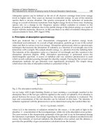
boundary conditions at the alignment layers, as illustrated in Fig. 1. Such a LC cell received
the name of twisted LC cell. The angle
between the directions of polishing is refered as
the twist angle.
A
y
A
d
A z
Φ
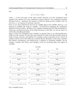
Fig. 1. Twist of LC molecules due to the boundary conditions at the alignment layers.
According to (Yariv & Yeh, 1984), the amplitude transmittance of twisted LC cell with front
molecules aligned along x-axis is given by the Jones matrix
sincossin
sinsincos
)exp()(
LC
i
i
iRJ
, (13)
where
)cos()sin(
)sin()cos(
)(
R
, (14)
is the coordinate rotation matrix and parameter
is defined as
22
. (15)
Using the Liquid Crystal Spatial Light
Modulators for Control of Coherence and Polarization of Optical Beams
311
Bellow we consider two important particular cases, namely when
º0
and
º90
. In the
first case we will reffer to the LC cell as 0º-twist LC cell and in the second case we will refer
to it as 90º-twist LC cell.
For 0º-twist LC cell Eq. (13) takes the form
10
0)2exp(
LC
i
J
. (16)
As can be seen from Eq. (16), the element
xx
j
of matrix
LC
J
describes the phase-only
modulation, and hence, under certain conditions, the 0º-twist LC cell can be used to provide
the modulation of coherence and polarization discussed in the previous section.
For 90º-twist LC cell Eq. (13) takes the form
sin
2
sincos
sincossin
2
)exp(
LC
i
i
iJ
, (17)
with
22
)2(
. (18)
As can be seen from Eq. (17), the general element
ij
j of matrix
LC
J
this time describes the
joint amplitude and phase modulation, and hence, the 90º-twist LC cell can not be directly
used to realize the modulation of coherence and polarization. Nevertheless, placing the 90º-
twist LC cell between a pair of polarizers whose main axes make angles
1
and
2
with x
direction, as is shown in Fig. 2, it is possible to achieve the phase-only modulation (Lu &
Saleh, 1990).
A
z
A y
Ψ
1
Ψ
2
Polarizer 1 90° LC cell Polarizer 2
Fig. 2. 90º-twist LC cell sandwiched between two polarizers.
The Jones matrix for the system shown in Fig. 2 is given by
)()(
1PLC2P
JJJT
, (19)
where
LC
J
is the matrix given by Eq. (17) and
Optoelectronics – Devices and Applications
312
2
2
P
sinsincos
sincoscos
)(J
(20)
is the Jones matrix of polarizer. On substituting from Eqs. (17) and (20) into Eq. (19) with
values
º0
1
and
º90
2
, we obtain
0sincos
00
)exp(
i
iT
. (21)
The matrix given by Eq. (21) contains the only non-zero element
sincos)exp( iit
yx
, (22)
which can be expressed in the complex exponential form
)(argexp
yxyxyx
titt
, (23)
with modulus
2/1
2
2
sin
2
1
yx
t
, (24)
and argument
tantan)(arg
1
yx
t
. (25)
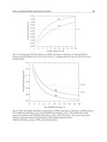
The quantities given by Eqs. (24) and (25), as functions of the birefringence parameter
with due regard for Eq. (18), are plotted in Fig. 3.
I
n
t
e
n
s
i
t
y
t
r
a
n
s
m
i
t
t
a
n
c
e
0
aπ
2
π
3
π
4
π
β
0.2
0.4
0.6
0.8
1
1
.
2
2
π
4
π
6π
8π
0
P
h
a
s
e
s
h
i
f
t
aπ
2
π
3
π
4
π
β
a) b)
Fig. 3. Complex transmittance given by Eq. (23): a) amplitude transmittance, Eq. (24); b)
phase transmittance, Eq. (25).
As can be seen from this figure, starting from some critical value of the birefringence
parameter
, approximately equal to
23
, the amplitude transmittance
yx
t
approachs to
Using the Liquid Crystal Spatial Light
Modulators for Control of Coherence and Polarization of Optical Beams
313
unity while the phase transmittance rises linearly having a slope of approximately
2
. Thus,
when the birefringence parameter satisfies the condition
23
, the matrix given by Eq.
(21) can be well approximated as
0)2exp(
00
i
T
, (26)
i.e. the 90º-twist LC cell sandwiched between two crossed polarizers can be considered as
the phase-only modulator.
Till now we assumed that parameter
characterizing the LC cell has a fixed value.
Nevertheless, as well known (Lu & Saleh, 1990) , applying to the LC cell an electric field
normal to its surface, the birefringence parameter is no longer constant and changes in
accordance with
dnn ])([)(
oe
, (27)
where
is the tilt of the LC molecules with respect to the z axis caused by the electric field.
Besides, the relationship between extraordinary refraction index and the molecular tilt can
be approximated as
o
2
oee
cos)()( nnnn
. (28)
It has been shown (Lu & Saleh, 1990) that the dependence between tilt angle and applied
voltage has the form
crms
0
crms
crms
rms
,exparctan2
2
,0
)(
VV
V
VV
VV
V
, (29)
where
c
V
is the threshold voltage,
0
V
is the saturation voltage, and
rms
V
is the effective
voltage. Combining Eqs. (27) – (29), it is possible to show that the birefringence parameter
finds to be approximately proportional to the inverse value of the applied voltage.
Finally, we are ready to define a LC-SLM as an electro-optical device composed by a large
number of LC cells (pixels) whose birefringence indices are controlled by the electrical
signals generated by computer and applied individually to each cell by means of an array of
electrodes. The amplitude transmittance of 0º-twist LC-SLM or 90º-twist LC-SLM can be
described by Eqs. (16) and (26), respectively, replacing parameter
by spatial function
)(x
.
4. Techniques for control of coherence and polarization by means of LC-
SLMs
4.1 Single 0º-twist LC-SLM
We begin with the technique based on the use of a 0º-twist LC-SLM (Shirai & Wolf, 2004). It
is assumed that the incident light represents a linear polarized laser beam characterized by
the cross-spectral density matrix
Optoelectronics – Devices and Applications
314
2
2
2
2
2
2
1
2
021
sinsincos
sincoscos
4
exp),(
xx
xxW E
, (30)
where
0
E is the value of power spectrum at the beam centre, ε is the effective (rms) size of
the source, and
is the angle that the direction of polarization makes with the x axis. It can
be readily verified that for such a beam
1),(
21
xx
and
1)(
xP
, i.e. the beam described by
Eq. (30) is completely coherent and completely (linearly) polarized.
If the extraordinary axis of the LC is aligned along the y direction the transmittance of 0º-
twist LC-SLM, in accordance with the previous section, is given by matrix
)](2exp[0
01
)(
1
1LC
x
xT
i
(31)
(here the subscript “1” is used for the sake of simplicity of posterior consideration). It is
assumed that the birefringence
)(
1
x
has the form
)(
2
1
)(
01
xx
, (32)
where
0
is a constant and
)(x
is a computer generated zero mean random variable which
is characterized by the Gaussian probability density
2
2
2
)(
exp
2
1
)(
x
xp
, (33)
with variance
22
)(
x
and cross correlation defined at two different points as
2
2
2
21
2
exp)()(
xx , (34)
where
21
xx
and
is a positive constant characterizing correlation width of
)(x
.
On substituting from Eqs. (30) - (32) into Eq. (10), one obtains
2
2
1
2
1
2
021
4
exp),(
xx
xxW E
2
2110
20
2
sin)]()([expsincos)](exp[)exp(
sincos)](exp[)exp(cos
xxx
x
iii
ii
. (35)
On making use of Eqs. (33) and (34), it can be shown that (Ostrovsky et al, 2009b, 2010)
2
exp)](exp[
2
xi
, (36)
2
2
2
2121
2
exp1exp)()(exp)()(exp
xxxx ii . (37)
Using the Liquid Crystal Spatial Light
Modulators for Control of Coherence and Polarization of Optical Beams
315
Then, Eq. (35) can be rewritten as
2
2
1
2
1
2
021
4
exp),(
xx
xxW E
2
2
2
2
2
0
2
0
2
sin
2
exp1expsincos
2
exp)exp(
sincos
2
exp)exp(cos
i
i
. (38)
To simplify the consequent analysis, we assume that
is large enough to accept the
following approximations (Shirai & Wolf, 2004):
0
2
exp
2
, (39)
2
2
2
2
2
2
exp
2
exp1exp
, (40)
where
. In this case Eq. (38) can be rewritten approximately as
.
sin
2
exp0
0cos
4
exp),(
2
2
2
2
2
2
1
2
1
2
021
xx
xxW E
(41)
According to definitions given by Eqs. (3) and (4), we find
2
2
2
sin
2
exp11)(
, (42)
2cos)(
xP
. (43)
Equations (42) and (43) show that the modulated beam is, in general, partially coherent and
partially polarized. The degree of polarization changes in the range from 1 to 0 with a
proper choice of polarization angle
of the incident beam. The degree of coherence, for a
fixed value of
can be varied by a proper choice of parameters
and
of the control
signal
)(x
, as it is shown in Fig. 4.
We would like to point out the following two shortcomings of the described technique.
Firstly, as can be seen from Eqs. (42) and (43) this technique does not provide the
independent modulation of the degree of coherence and the degree of polarization since
both of them depend at the same time on the polarization angle
. Secondly, as can be seen
from Fig. 4, this technique does not allow to obtain the values of the degree of coherence in a
whole desired range from 1 to 0.
Optoelectronics – Devices and Applications
316
Fig. 4. Degree of coherence given by Eq. (42) for
4
and different values of
.
4.2 Two 0º-twist LC-SLMs coupled in series
To avoid the shortcomings mentioned above, the authors (Ostrovsky et al, 2009) proposed to
use instead of a single 0º-twist LC-SLM the system of two 0º-twist LC-SLMs coupled in
series as shown in Fig. 5.
Fig. 5. System of two crossed 0º-twist LC-SLMs coupled in series. The bold-faced arrows
denote the extraordinary axis of liquid LC.
The transmittance of the first SLM is just the same as in previous technique, while the
transmittance of the second one, whose extraordinary axis is aligned in the x direction, is
given by matrix
10
0)](2exp[
)(
2
2LC
x
xT
i
, (44)
Using the Liquid Crystal Spatial Light
Modulators for Control of Coherence and Polarization of Optical Beams
317
where birefringence
)(
2
x
has the form
)(
2
1
)(
02
xx
, (45)
with
0
and
)(x
of the same meaning as stated in the context of Eq. (32). The transmittance
of the system composed by two crossed 0º-twist LC-SLMs is given by matrix
)](exp[0
0)](exp[
)exp()()()(
01LC2LC
x
x
xTxTxT
i
i
i
. (46)
On substituting from Eqs. (30) and (46) into Eq. (10) with due regard for relation (37), one
obtains
2
2
1
2
1
2
021
4
exp),(
xx
xxW E
2
2
2
2
2
2
2
2
2
22
2
2
2
sin
2
exp1expsincos
2
exp1exp
sincos
2
exp1expcos
2
exp1exp
(47)
and then, using approximations (39) and (40),
.
sin0
0cos
2
exp
4
exp),(
2
2
2
2
2
2
1
2
1
2
021
xx
xxW E (48)
According to definitions given by Eqs. (3) and (4), we find
2
2
2
exp)(
, (49)
2cos)(
xP
. (50)
As can be seen from Eqs. (49) and (50), the output degree of coherence in this case does not
depend on direction of the input polarization and changes in the whole desired range from
1 to 0.
4.3 Two 0º-twist LC-SLMs coupled in parallel
The result resembling the one given above can be also obtained using the system of two 0º-
twist LC-SLMs coupled in parallel. Such a system has been described in (Shirai et al, 2005).
Here we propose a somewhat modified version of this technique.
The technique is based on the use of two 0º-twist LC-SLMs with orthogonal orientations of
their extraordinary axes placed in the opposite arms of a Mach-Zehnder interferometer as it
is shown in Fig. 7. The polarizing beam splitter at the interferometer input separates the
orthogonal beam components
)(x
x
E
and )(x
y
E so that each of them can be independently
Optoelectronics – Devices and Applications
318
Fig. 6. Degree of coherence given by Eq. (49) for
4
and different values of
.
Fig. 7. System of two crossed 0º-twist LC-SLMs coupled in parallel: PBS, polarizing beam
splitter; M mirror; BS beam splitter. The bold-faced arrows and circled dots denote
polarization directions.
modified by different LC-SLMs. The modified beam components are superimposed in the
conventional beam splitter at the interferometer output. Disregarding the negligible changes
of coherence and polarization properties of the electromagnetic field induced by the free
space propagation within the interferometer, one can represent the considering system as a
thin polarization-dependent screen with the transmittance given by matrix
)](2exp[0
0)](2exp[
)(
2
1
x
x
xT
i
i
. (51)
As before, we assume that parameter
of each 0º-twist LC-SLM has the form
)(
2
1
)(
)2(10)2(1
xx
, (52)
Using the Liquid Crystal Spatial Light
Modulators for Control of Coherence and Polarization of Optical Beams
319
with
0
and )(
)2(1
x
of the same meaning as stated in the context of Eq. (32). It is assumed
also that the variables
)(
1
x
and
)(
2
x
are generated by two different computers so that
they can be considered as statistically independent with the separable joint probability
density
)()()()(
2121
xxxx
ppp
. (53)
Following Subsection 4.1 and using in addition relation (Ostrovsky et al, 2010)
2
1)1(22)2(1
exp)]}()([exp{
xxi
, (54)
it may be readily shown that the cross-spectral density matrix
),(
21
xxW
, the degree of
coherence
),(
21
xx
and the degree of polarization
)(xP
, in this case, are just the same as
ones given by Eqs. (48) – (50).
4.4 Two 90º-twist LC-SLMs coupled in parallel
The considered above techniques for modulation of coherence and polarization are based on
the use of 0º-twist LC-SLMs. The consistence of these techniques is well grounded in theory
but no relevant experimental results have been yet reported. This situation can be explained
by the lack at present of commercial 0º-twist LC-SLMs with the required characteristics.
Here we propose an alternative technique which uses widely available commercial 90º-twist
LC-SLMs and, hence, can be easily realized in practice. The proposed technique is sketched
schematically in Fig. 8.
In spite of its outward resemblance with the technique described in the previous subsection,
this technique has two essential distinctions. Firstly, instead of 0º-twist LC-SLMs here the
orthogonally aligned 90º-twist LC-SLMs are used in the opposite arms of the Mach-Zehnder
interferometer. Secondly, the conventional beam splitter at the output of interferometer is
replaced by the polarizing one. As a result, taking into account that two polarizing beam
splitters coupled in series act as crossed polarizers, each arm of interferometer can be
considered as the system shown in Fig. 2 with
º0
1
and
º90
2
. In accordance with
Section 3 such a system realizes the phase-only modulation of the correspondent orthogonal
component of the incident beam.
Fig. 8. System of two crossed 90º-twist LC-SLMs coupled in parallel: PBS, polarizing beam
splitter; M, mirror. The bold-faced arrows and circled dots denote polarization directions.
Optoelectronics – Devices and Applications
320
Again disregarding the negligible changes of coherence and polarization properties of the
electric field induced by the free space propagation within the interferometer, the system
shown in Fig. 8 can be considered as a thin polarization-dependent screen with
transmittance given by matrix
0)](2exp[
)](2exp[0
)(
1
2
x
x
xT
i
i
, (55)
where
)(
)2(1
x
has the same meaning as in Eq. (51). It can be readily shown that for this
technique the cross-spectral density matrix has a slightly different form, namely
2
2
2
2
2
2
1
2
1
2
021
cos0
0sin
2
exp
4
exp),(
xx
xxW E , (56)
but the degree of coherence
),(
21
xx
and the degree of polarization
)(xP
are given again
by Eqs. (49) and (50).
Concluding, it is appropriate to mention here that the proposed technique, as well the one
presented before, provides generating the beam of a Gaussian Schell-model type given by
Eq. (6) with parameters
22
00
sinES
x
,
22
00
cosES
y
and
yx
.
5. Measurements of coherence and polarization
In practice the efficiency of the techniques described in previous section can be verified by
measuring the degree of coherence and the degree of polarization of modulated
electromagnetic beam. The main idea of such a measuring is well known (Wolf, 2007) and
consists in the implementation of four two-pinhole Young’s experiments with different
states of polarization of the radiation emerged from each pinhole. Nevertheless, the practical
realization of such an idea proves to be difficult in consequence of physical impossibility to
insert the needed optical elements just behind the pinholes. Here we present the technique
for measuring the degree of coherence and the degree of polarization proposed by the
authors (Ostrovsky et al, 2010), which permits to avoid this difficultness.
The technique consists in applying the Mach-Zehnder interferometer shown in Fig. 9. This
allows the physical insertion of the appropriate optical elements for simultaneous and
independent transforming the orthogonal beam components. The polarizers P
1
and P
2
serve
to cut off only one of the orthogonal field components, while the removable rotators R
1
and
R
2
serve to produce the rotation of one of the transmitted field component through 90˚ (for
such a purpose a suitably oriented half-wave plate can be used). The operation description
of the technique is given bellow.
The determination of the elements
ij
W
of the matrix
),(
21
xxW
is realized by means of the
following four experiments. In the first experiment the polarizers P
1
and P
2
are aligned to
transmit only x components of the incident field without any subsequent rotation of the
plane of polarization. In the second experiment P
1
and P
2
are aligned to transmit only y
components of the incident field again without any subsequent rotation of the plane of
polarization. In the third and the fourth experiments the polarizers P
1
and P
2
cut off the
different orthogonal components of the incident field and the corresponding polarization
rotator R
1
or R
2
serves to allow the interference of these components.
Using the Liquid Crystal Spatial Light
Modulators for Control of Coherence and Polarization of Optical Beams
321
Fig. 9. System for measuring the statistical properties of modulated beam: BS, beam splitter;
M, mirror; TP, translating pinhole; P
1
, P
2
, polarizers; R
1
, R
2
; polarization rotators.
The spectral density or power spectrum of the field observed at the output of the
interference system in each experiment can be described by the spectral interference law,
which under certain conditions can be written as (Wolf, 2007)
,),,(
22
cos
22
2
22
)(
0
yxji
ξ
,
ξ
αx
z
kξξ
,
ξ
W
ξ
S
ξ
SxS
ijijjiij
(57)
where
i
S
and
j
S
are the power spectra of the field components in the pinhole position
2ξ/
,
k is the wave number,
0
z
is the geometrical path between the pinhole plane and the
observation plane, and
.arg
ijij
Wα
From the physical point of view, Eq. (57) describes an
image with periodic structure, known as the interference fringe pattern. The measure of the
contrast of the interference fringes is the so-called visibility coefficient defined as
.
)()(
)()(
)(ξ
minmax
minmax
xSxS
xSxS
V
ijij
ijij
ij
(58)
On substituting from Eq. (57) with
1).cos(
into Eq. (58), we readily find that
ξ)V
ξ
S
ξ
SξW
ijjiij
(
222
1
)(
. (59)
The spectra
i
S
and
j
S
can be easily measured when one of the pinholes is covered by an
opaque screen. The phase
ij
α can be measured by determining the location of maxima in the
interference pattern. Hence, measuring in each experiment the visibility
,
ij
V
power spectra
,
)( ji
S
and phase
ij
α , one can determine all the elements
ij
W
of the matrix
),(
21
xxW
. The
degree of coherence and the degree of polarization of the modulated beam can be then
calculated using definitions given by Eqs. (3) and (4).
Optoelectronics – Devices and Applications
322
6. Experiments and results
To verfy the proposed technique in practice, we conducted some physical experiments. The
experimental setup used in experiments is sketched in Fig. 10. The principal part of the
experimental setup was composed of two Mach-Zehnder interferometers coupled by the
common beam splitter. The first interferometer realized the modulation of the incident beam
as it has been described in Subsection 4.4, while the second one served for measuring the
degree of coherence and the degree of polarization of the modulated beam as it has been
described in Section 5.
As the primary source we used a highly coherent linearly polarized beam generated by He-
Ne laser (Spectra-Physics model 117A, λ=633 nm, output power 4.5 mW) which can be well
described by the model given by Eq. (30). The laser was mounted in a rotary stage that
allowed changing the polarization angle
without any loss of light energy. As the 90º-twist
nematic LC-SLMs we used the computer controlled HoloEye LC2002 electro-optical
modulators which have resolution of 800 × 600 pixels (32 µm square in size) and can display
the control signal with 8 bit accuracy (256 gray levels). The control of LC-SLMs was realized
independently by two computers using a specially designed program for generating the
random signals which obey the desired Gaussian statistics. To realize the measurements of
the degree of coherence we used two pinholes with diameter of 200 µm mounted on
motorized linear translation stages.
Fig. 10. Experimental setup: L, laser; BE, beam expander; ZL, zoom-lens; PD, photodiode;
the other abbreviations are just the same as in Figs. 8 and 9.
We realized two sets of experiments. In the first set we measured the degree of polarization
for different values of the polarization angle of incident beam and for the fixed value (
1
)
Using the Liquid Crystal Spatial Light
Modulators for Control of Coherence and Polarization of Optical Beams
323
of parameter
of the control signal. The results of these experiments are shown in Fig. 11.
In the second set we chosed
4
and measured the degree of coherence varying the
parameters
and
of the control signal to ensure the chosen values of parameter
.
The results of these experiments are shown in Fig. 12. As a whole, the results obtained in
both sets of experiments are in a good accordance with theoretical predictions.
Fig. 11. Results of measuring the degree of polarization for
1
.
Fig. 12. Results of measuring the degree of coherence for
4
and different values of
parameter
.
7. Conclusion
In this chapter the problem of modulating the coherence and polarization of optical beams
has been considered. It has been shown that the LC-SLM represents an ideal tool for
practical realizing such a modulation. We have analized the known techniques of optical
modulation based on the use of 0º-twist LC-SLM and have proposed a new technique based
on the use of two 90º-twist LC-SLMs. Because of the wide commercial availability of 90º-
Optoelectronics – Devices and Applications
324
twist LC-SLMs the proposed technique proves to be the most attractive one. The
justifiability of this technique has been corroborated by the results of physical experiments.
8. Acknowledgment
The authors gratefully acknowledge the financial support from the Benemérita Universidad
Autónoma de Puebla under project VIEP: OSA-EXT-11-G.
9. References
Goodman, J. W. (1996). Introduction to Fourier Optics (2
nd
Edition), McGraw-Hill, ISBN 0-07-
024254-2, USA.
Lu, K. & Saleh B. E. A. (1990). Theory and design of the liquid crystal TV as an optical spatial
phase modulator. Optical Engineering, Vol.29, No.3, (March 1990), pp. (240-246).
ISSN 0091-3286.
Ostrovsky A. S. (2006). Coherent Mode Representations in Optics, SPIE Press, ISBN 0-8194-6350-
7, Bellingham WA, USA.
Ostrovsky A. S. ; Martínez-Vara P. ; Olvera-Santamaría M. Á. & Martínez-Niconoff G.
(2009a). Vector coherence theory : An overview of basic concepts and definitions,
In: Recent Research Developments in Optics, S. G. Pandalai, (113-132), Research
Singpost, ISBN 978-81-308-0370-8, Kerala, India
Ostrovsky A. S.; Martínez-Niconoff G.; Arrizón V.; Martínez-Vara P.; Olvera-Santamaría M.
Á. & Rickenstorff C. (2009b). Modulation of coherence and polarization using
liquid crystal spatial light modulators. Optics Express, Vol.17, No.7, (March 2009),
pp. (5257-5264). ISSN 1094-4087.
Ostrovsky A. S.; Rodríguez-Zurita G.; Meneses-Fabián C.; Olvera-Santamaría M. Á. &
Rickenstorff C. (2010). Experimental generating the partially coherent and partially
polarized electromagnetic source. Optics Express, Vol.18, No.12, (June 2010),
pp.(12864-12871). ISSN 1094-4087.
Shirai T. & Wolf E. (2004). Coherence and polarization of electromagnetic beams modulated
by random phase screens and their changes on propagation in free space. Journal of
the Optical Society of America A, Vol.21, No.10, (October 2004), pp. (1907-1916). ISSN
1084-7529.
Shirai T.; Korotkova O. & Wolf E. (2005). A method of generating electromagnetic Gaussian
Schell-model beams. Journal of Optics A: Pure and Applied Optics, Vol.7, No.5, (March
2005), pp. (232-237). ISSN 1464-4258.
Wolf E. (2007). Introduction to the Theory of Coherence and Polarization of Light, Cambridge
University Press, ISBN 9780521822114, Cambridge, UK.
Yamauchi M. & Eiju T. (1995). Optimization of twisted nematic liquid crystal panels for
spatial light phase modulation. Optical Communications, Vol.115, No.1, (March
1995), pp. (19-25). ISSN 0030-4018.
Yariv, A. & Pochi, Y. (1984). Optical Waves in Crystals, Wiley, ISBN 0-471-09142-1, USA.
16
Recent Developments in
High Power Semiconductor Diode Lasers
Li Zhong and Xiaoyu Ma
National Engineering Research Center for Optoelectronic Devices,
Institute of Semiconductors, Chinese Academy of Sciences
Beijing
China
1. Introduction
Due to a number of advantages of diode lasers, such as small size, light weight, high
efficiency etc., it has been the focus of the laser field from the beginning of the birth and has
been widely used in industrial, military, medical, communications and other fields.
Especially, to a great extent, a tremendous growth in the technology of solid-state lasers has
been complemented by laser diode array designs for pumping such solid-state lasers.
Significant applications continue to exist at common solid state laser systems such as
yttrium aluminum garnet doped with neodymium or ytterbium (Nd:YAG or Yb:YAG,
respectively) requiring pump light in the 780 nm to 1000 nm range. Driven by the increasing
demands of high-performance high-power laser pumping source and direct industrial
processing applications, tremendous breakthrough have been realized in the main optical-
electronic performances of high power semiconductor diode lasers, such as ultra-high peak
power, super-high electro-optical conversion efficiency, low beam divergence, high
brightness, narrow spectrum linewidth, high operation temperature, high reliability,
wavelength stabilization and fundamental transverse mode operation etc. These
achievements are attributed to a combination of the maturity of semiconductor material
epitaxy, the optimization of the laser waveguide structure, the cavity surface-passivation
technology as well as the high effective cooling and packaging technologies. The Occident
and Japan keep ahead in this field with several large corporations actively engaged in this
market, for example, Coherent, IMC, SDL, OPC, HPD, Spectrum-Physics of the U.S.,
OSRAM, JOLD, Frauhorf of Germany, THALES of France, SANYO, SONY of Japan, and
ATC of Russia etc. The wavelength of these industrial products ranges from 630 nm to
1550 nm, and optical output power levels from several W to 10 kW class. In China,
prominent progresses have also been made at a rapid rate. Advances in the design and
manufacture of the bars, together with effective means of stacking and imaging monolithic
semiconductor laser arrays (bars), have enabled the production of robust sources at market-
competitive costs. In particular, the diode lasers for these systems have to meet high
demands in relation to efficiency, power, reliability and manufacturability, which following
the desire for reducing the cost per watt and the cost per hour’s lifetime for the customer.
However, with the enhancement of the power and beam quality, a series of new practical
problems arise in the aspect of engineering, such as high cost of the high-current and low-
Optoelectronics – Devices and Applications
326
voltage power supply and short life span of micro-channel heat sink cooling etc Gradually,
single-emitter semiconductor laser devices and mini-bars with high power and high beam
quality are becoming the mainstream research trend and replacing the traditional cm-bars.
On the other hand, the reduced divergence angle accelerates the improvement of beam
quality, which is directly reflected in the decrease of the fiber diameter and the increase of
the output power for fiber-coupled diode laser module. Here we review and discuss the
state of the art of high power semiconductor diode lasers, including single emitters, bars,
horizontal bar arrays and vertical bar stacks, with the typical data presented. Several key
technological problems concerning the improvements of diode lasers performance, the
optimization of packaging architectures and the developments of high beam quality of
diode lasers will be discussed in section 2~5, respectively. In section 6, we conclude with
some thoughts on the future study directions and the developing tendency for high power
diode lasers.
2. Status of high-power diode laser technology and characteristics
2.1 Laser diode chip technology
Over the recent years, high power diode lasers have seen a tremendous evolution in
material epitaxial growth technology, epi-structure optimization technique, cavity surface-
passivation technology etc Epitaxial structure is designed for a specific range of operation
to optimize a combination of optical, electrical and thermal performance, generally
minimizing both operating voltage and internal loss to achieve high efficiency with long
cavities for high-average-power and high-brightness applications. The details of these
structures, such as material compositions, layer thicknesses, asymmetric or symmetric
waveguide structure design, and doping profiles are selected to ensure that
manufacturability and reliability are not compromised. Important developments in epitaxial
growth technology include the reporting of low loss materials (about 1 cm
–1
for AlGaAs for
example), the development of the strained materials with attendant benefits on gain and
bulk defect pinning, and the development of aluminum-free materials such as InGaAs and
InGaAsP with the latter material having been reported to wavelengths below 800 nm. A
number of careful studies are being reported on filament formation and current crowding in
semiconductor lasers and methods for avoiding their deleterious effects. With the
improvement of the high-quality, low defect density epitaxial growth technology of
semiconductor materials, the resonator cavity length of the existing cm bar has been
increased from 0.6 ~ 1.0 mm to 2.0 ~ 5.0 mm, making a significant increase of the output
power. The large cavity length ensured low thermal and electrical resistivities of the devices
by increasing their active area. The cavity length is selected mainly depending on desired
operation power and is optimized for best power conversion efficiency (PCE) at the given
condition.
In continuous wave (CW) operation the output power from high power laser bars usually is
limited by the thermal load that the assembly may dissipate. Failure modes, like wear out of
the output power or bulk failures are critical in CW operation. For quasi continuous wave
(qCW) applications the reliable output power in general is not thermally limited. The
robustness of the output facet of the devices and the degradation of the assembly under the
cyclic thermal load become the critical matter. Special methods of facet design and treatment
have been employed to increase the COMD power threshold and suppress its degradation
over the operating life of the device, such as facet passivation with a dielectric layer,
Recent Developments in High Power Semiconductor Diode Lasers
327
regrown non-absorbing mirror (ReNAM), intermixed non-absorbing mirror (iNAM), ultra-
high vacuum (UHV) cleaved facets etc (Yanson et al., 2011) NAM-based techniques
(ReNAM and iNAM) require further development to achieve required reliability figures.
Dielectric passivation and cleave-in-a-vacuum techniques are found to be the two best
performing facet engineering solutions. At 980nm, dielectric facet passivation can be
employed with a pre-clean cycle to deliver a device lifetime in excess of 3,000 hours at
increasing current steps. Vacuum cleaved emitters have delivered excellent reliability at
915nm, and can be expected to perform just as well at 925 and 980nm. By preventing
exposure of a freshly cleaved facet to oxygen, the formation of surface oxides and shallow
levels is avoided without the need for ion plasma cleaning.(Tu et al., 1996) A capping layer,
also deposited in a vacuum, seals the facet and stops the penetration of oxygen. Single
emitters fabricated with these two techniques are packaged into fiber-coupled modules with
10W output and 47% efficiency. (Tu et al., 1996)
2.2 Far field divergence angle control
As the basic unit of the integration of semiconductor laser system, the performance of
different structure and different types of semiconductor laser device directly contributes
to the development of semiconductor laser systems, one of the most important
developments is the reduction of the beam divergence and the increase of the output
power. According to the definition of the beam quality, the beam divergence angle is
proportional to the beam-parameter product (Q or BPP), which is a measure of the beam
quality. Therefore the beam quality is under the direct control of the far field divergence
angle. Overall, the waveguide structure of semiconductor lasers leads to a serious
asymmetry far-field beam quality. In the fast axis direction, the output beam can be
considered to be fundamental mode, but the divergence angle is large. The compression
of the fast axis divergence angle can effectively reduce the requirements for the fast axis
collimator aperture. While in the slow axis direction, the output beam is multi-mode and
the beam quality is poor. The beam quality can be directly improved by reducing the
divergence angle in the slow axis direction, which is the research focus in the field of the
high-beam quality semiconductor laser.
The research focus in the control of the fast axis divergence angle is how to balance the
fast axis divergence angle and the electro-optical conversion efficiency. Although a
number of research institutions had press release of the continued access to fast axis
divergence angle of only 3° and even 1°, but based on the consideration of the power, the
electro-optical conversion efficiency and the cost, it is difficult to promote practical
applications in the short term. In the early year of 2010, the P. Crump etc. of German
Ferdinand-Braun Institute has reported the fast axis divergence angle of 30° (95% of the
energy range) obtained through the use of large optical cavity and low-limiting factors,
meanwhile the electro-optical conversion efficiency of the device is 55%, which is the basic
standards to practical devices. The fast axis divergence angle of the current commercial
high-power semiconductor laser devices are also dropped from the original of about 80°
(95% of the energy range) to below 50°, which substantially lower the requirements for the
numerical aperture of the collimator.
In the slow-axis divergence angle control, recent studies have shown that, in addition to
the device's own structure, the combination of the drive current density and the thermal
effects of semiconductor lasers affect the slow axis divergence angle. The slow axis
divergence of a single emitter with long cavity length is of the most easy to control,
Optoelectronics – Devices and Applications
328
whereas in the array device, with the increase of the fill factor, the intensification of
thermal cross-talk between the emitting elements will lead to the increase of the slow-
axis divergence angle. In the year of 2009, the Bookham company of Switzerland has
successfully reduced the slow-axis divergence (95% of the energy range) of 9xx-nm 10
W commercial devices with 5 mm cavity length from 10
o
~ 12
o
to about 7
o
. In the same
year, the Osram Company of German and the Coherent Company of the United States
has reduced the slow-axis divergence of the array (95% of the energy range) to 7
o
level.
2.3 High-temperature performance of laser bars and arrays
Since the performance of a diode laser is operating temperature dependent, high-power
diode laser pump modules usually need a cooling system to control their operating
temperature. However, some diode laser applications require that high-power diode laser
pump modules operate in a high temperature environment without any cooling. In
addition, the diode laser pump modules have to provide both high peak power and a nice
pulse shape because certain energy in each pulse is required. At such a high temperature,
semiconductor quantum well gain drops significantly, and the carrier leakage and the
Auger recombination rate increases. Thus, the laser bar has a high threshold and low
slope efficiency, resulting in very low power efficiency. To reach certain power level at
high temperature, the pump current has to be much higher than that at room temperature.
More waste heat is generated in the active region of the diode laser bar. In addition, tens
of milliseconds pulse width with a few percent duty cycle forces the laser bar to operate in
a “CW” mode.(Ziegler et al., 2006; Puchert et al., 2000; Voss et al., 1996) The Lasertel
Company has presented the development of high-temperature 8xx-nm diode laser bars
for diode laser long-pulse (>10 milliseconds) pumping within a high-temperature (130 ºC)
environment without any cooling.( Fan et al., 2011) The epi-structure is based on a large
optical cavity separate confinement heterostructure with Al-free active region. By
adjusting Aluminum concentration in the AlGaInP barrier, introducing strain in quantum
well (QW) and adjusting the width of QW, optimizing the strain and the width of
quantum well, the gain is maximized, the loss and carrier leakage especially at high
temperature is minimized and the optical confinement of the waveguide is also be
improved. Under the operation condition (130 ºC, 15 ms pulse width, 5 Hz frequency and
100-A current pulse), the high-temperature laser bars show robust and consistent
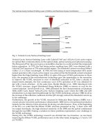
performance, reaching 60 W (peak) power and having good pulse shape, as shown in
Figure 1. The laser bars do not show any degradation after 310,000 15-millisecond current
pulse shots. They demonstrated over 40-millisecond long-pulse operation of the 8xx-nm
CS bars at 130 ºC and 100 A. Regardless of the pulse shape, this laser bar can lase at
extremely high temperature and output pulse can last for 8 ms/2ms at 170 ºC/180 ºC
respectively, both driven by 60 A current pulses with 5-Hz frequency, 10 millisecond
pulse width. This is the highest operating temperature for a long-pulse 8xx-nm laser bar.
Figure 2 shows the high-temperature performance of the 3-bar stack array and its pulse
shape at 130 ºC. The peak power of the 3-bar array reaches 165 kW at 100A and 130 ºC, but
the pulse shape is very sensitive to the current and the power of the array drops much
faster than that of the CS bar, which may be attributed to the package difference between
the CS bar and stack array.
Recent Developments in High Power Semiconductor Diode Lasers
329
Fig. 1. Pulsed (15 msec PW and 5 Hz frequency) L-I performance and wall-plug efficiency at
130°C.
Fig. 2. High temperature performance of 3-bar array (left) and its pulse shape at 130 ºC
(right).
3. The latest high-power semiconductor laser devices
3.1 Developments of the standard cm laser diode bar
The increasing of reliable power level of diode lasers will enable wider deployment, higher
power systems and new market which were previously unavailable, such as direct materials
processing etc. Also, it will lead to lower cost to the user, per watt of useable output. The
standard length of the laser bars of 1 cm array has been established to obtain high power
output, i.e. many emitters has been lateral parallel monolithic integrated in the scale of the
slow axis direction into one diode laser bar, Laser bars provide a magnitude of output
power of single emitter by integration the single emitters at the wafer level, which has long
been a most commonly used form for high-power semiconductor lasers. According to the
application, whether high brightness or high power operation is intended, the filling factor
is varied between 10% to 80%.
In the early year of 2008, the Spectra-Physics Company of the United States reported the
access of 800 W/bar, 1010 W/bar, 950 W/bar maximum output power respectively from the
center wavelength of 808 nm, 940 nm, 980 nm cm bar, with corresponding maximum PCE
Optoelectronics – Devices and Applications
330
values of 54.3%, 67.4%, and 70%. (Li et al., 2008) Figure 3 summarizes the P-I-PCE curves of
bars.
Fig. 3. P-I-PCE curves of bars with double-side cooling from the Spectra-Physics Lasers
Company.
All of the bars had a FF of 83% (65 emitters, each 125-μm wide and 5.0-mm long, with a
separation of 150 μm). All bars were bonded using the double-sided micro-channel heat sink
cooling technology with the circulating water at 5-8°C (Li et al., 2008). These output power
are the maximum continuous output power level of the current laboratory. In addition,
many other semiconductor laser company, such as the German company JENOPTIK,
Switzerland company Oclaro also continued to prepare the kilowatt diode laser array. J.
Müller ect. of the Oclaro has made it clear that the access to 1.5 kW/bar array devices is not
a problem based on the existing technologies. At the same time, the output power of high
beam quality, low fill factor cm bar is also increasing. Table 1 gives the BPP value of cm bars
with different fill factors obtained by the Limo Company of German. From the results of
Table 1, it can be concluded that for a certain horizontal dimensions of semiconductor laser
array device, in the case of the same divergence angle, the BPP value is proportional to the
fill factor, i.e. the lower the fill factor, the smaller of the BPP value, and the better the beam
quality. Currently, In the 9xx-nm wavelength range 150 W or higher CW output power
levels have become the standard for high filling factor bars.( Lichtenstein et al., 2005; Krejci
et al., 2009; Crump et al., 2006) In the 80x range devices with 100 W and more output power
were demonstrated (Tu et al., 1996; Ziegler et al., 2006). The output characteristic of an 808
nm device optimized for 140-160 W CW output power is shown in Figure 4 (Müller et al.,
2010).An output power of 185 W is achieved for CW 200A drive current. For currents above
180 A the thermal limitation of the device is clearly visible in a pronounced rolling of the P-I
curve limiting the achievable brightness in this operation mode. The output power of 9xx-
nm cm bar with 20% fill factor is up to 180 W/bar in CW condition, the BPP value is down
to 5.9 mm·mrad after the symmetry of the fast and slow axis of the beam, and the
commercial devices can be work above the level of 80 W/bar with long-term stability; the
Recent Developments in High Power Semiconductor Diode Lasers
331
Emitter Width
(μ
m
)
100
200
150
100
5
Pitch
(μ
m
)
200
400
500
500
200
Number of Emitters
49
24
19
19
49
Fillin
g
Factor
(
%
)
50
50
30
20
2.5
Beam Diver
g
ence FA
(
FW 90%
)
(
°
)
80 80 80 80 80
Beam Diver
g
ence SA
(
FW 90%
)
(
°
)
12 12 12 12 12
BPP FA
(
mm·mrad
)
0.35 0.35 0.35 0.35 0.35
BPP SA
(
mm·mrad
)
257 251 149 100 13
Ratio
BPP SA/BPP FA
735 720 428 285 37
S
y
mmetrized BPP
(
mm·mrad
)
9.5 9.4 7.2 5.9 2.1
Beam Diameter at
NA=0.22
(μ
m
)
121 120 92 75 27
Table 1. the BPP of cm bars with different structures.
output power of 2.5 % fill factor cm bar is up to 50 W/bar in CW condition, the BPP value is
down to 2.1 mm·mrad after the symmetry of the fast and slow axis of the beam, the current
device is still under developing, and need to improve the stability further. The reliable output
power of CW operated bars is in first place limited by the cooling capability of the assembly.
Bars operated in a qCW mode deliver a significantly higher reliable output power, because the
thermal load is reduced by a factor which is inverse proportional to the duty cycle of the
operation mode. Figure 5 and 6 give the typical performance of our lab’s 808nm laser diode
bar packaged by conductive heatsink (qCW 300 W/barand 200 W/bar with 60% PCE) and
980nm laser diode bar packaged by micro-channel heatsink (CW 200W/bar), respectively.
Fig. 4. PIV-PCE characteristic of a 50% filling factor 808 nm bar on micro channel cooler at 25
°C water temperature from the Oclaro Company.
Optoelectronics – Devices and Applications
332
Fig. 5. The typical P-I-V curve and spectrum of 808-nm bar packaged by conductive heatsink
in our lab. (a) qCW 300 W/barand (b) qCW 200 W/bar with 60% PCE
Fig. 6. The typical P-I curve of CW 200 W/bar 980-nm bar packaged by microchannel
heatsink in our lab.
However, with the requirement for the decrease of the fill factor to increase the output
power and increase the beam quality, a series of new problems arise gradually, especially
high cost problem of its accompanying high-current and low-voltage power supply and
short life span problem of the micro-channel heat sink cooling etc. Most of the power test of
cm bar is subject to the limit of maximum current supply, instead of its own output power
limit. In engineering, a combination of several volts with several hundreds of current will
produce many practical problems. On the other hand, the micro-channel heat sink must be
used to dissipate the high heat flux generated by the cm bar with ultra-high power and high
beam quality, but the utmost ability of heat dissipation for the existing water-cooled micro-
channel heat sink is no doubt become the biggest obstacle for the further improvements of
power and beam quality. The recent developed double-sided micro-channel cooling
technology has limited effect on reducing the thermal resistance, and it doesn’t seem to
satisfy the sustainable expansibility for the power enhancement of the cm bar. In addition, it
also can not be ignored that the relatively short life span of the micro-channel heat sink has
been the current bottleneck for high-power semiconductor lasers. Although there are some
other new efficient technologies arise, such as phase change thermal cooling, spray cooling
Recent Developments in High Power Semiconductor Diode Lasers
333
and micro-heat-pipe technology etc., it is difficult to satisfy the practical applications in the
short term because of the performance characteristics, the cost and the compatibility
problems. Due to the two constraints mentioned above, in recent years, the major research
institutions and high-power semiconductor laser suppliers no longer blindly pursue the
improvement of the output power of cm bars, but gradually shift the focus to develop single
emitter and mini bars with high power and good beam quality.
3.2 Developments of the single emitter
Compared with the cm bar, the single emitter, which possesses the independent electrical
and thermal operation environment, can avoid the thermal crosstalk between the emitting
units, so that to have the obvious advantages in life span and beam quality. In addition,
owing to the low drive current of the single emitter, the requirement for the drive power can
be reduced significantly even in the serial operation. Meanwhile, the heat from a single
emitter is relatively low, so the conduction heat sink can be used directly for heat dissipation
to avoid the short life span problem brought by the micro-channel heat sink. And the
independent thermal operation environment can make it operate under high power density.
Currently, optical power linear density of a single emitter can be up to above 200 mW/μm
with narrow spectral width, while that of a cm bar is only about 50~85 mW/μm. Especially,
the independent thermal and electrical operation environment can make a significant
reduction in the risk of device failure. Under the support of the high stable gold tin solder
packaging technology, average life of the commercial high-power single emitters can reach
to above 100 thousands hours, which is much higher than that of cm bars and hence reduces
the use-cost of devices. Based on the advantages listed above, the single emitter exhibits the
trend that it will replace the cm bar gradually to become the mainstream semiconductor
laser device with high power and high beam quality.
In recent years, single emitters have been developed rapidly. Especially driven by the
demand of high power fiber lasers for high-brightness fiber-coupled pumping modules, the
single emitters with 90~100 μm strip width, which is matched to the 105 μm/125 μm
multimode fiber tail, are improved significantly in output power and beam quality.
Currently, the continuous output power of 9xx-nm single emitters can reach 20~25
W/emitter; while that for 8xx-nm can be also beyond 12 W/emitter. In terms of the
commercial devices, the 9xx-nm single emitters with the stripe width of 90~100 μm,
prepared by IPG, Oclaro, JDSU and other high-power semiconductor laser device suppliers,
can operate continuously and steadily over 10 W/emitter, and above 100 W output power
can be achieved from the synthesis of the fiber-coupled multiple single emitters.
3.3 Developments of the mini-bar devices
Although the output power of the single emitter is improved rapidly, there is still a wide
gap compared to the cm bar. To meet the needs of different applications on power, mini-bar,
a new type of high-power semiconductor laser devices, appears and is being developed
rapidly. The mini-bar is obtained by integrating several single emitters on a substrate, which
is actually the compromise and optimization in the structure of the cm bar and the single
emitter. It combines the advantages of the cm bar and the single emitter, and its drive
current, lifetime, output power density and spectral width are between those of the cm bar
and the single emitter. Also taking into account the high beam quality and the demand for
fiber laser pumping source, the development of the mini-bar mainly focuses on the low fill