Optoelectronics Materials and Techniques Part 7 pptx
Bạn đang xem bản rút gọn của tài liệu. Xem và tải ngay bản đầy đủ của tài liệu tại đây (7.3 MB, 30 trang )
Optoelectronics - Materials and Techniques
170
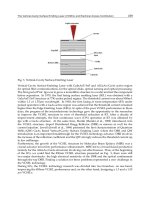
contains an interfacial layer on the silicon surface. However, in the present work, we could
not observe any interfacial layer on the silicon surface (Fig.5). Figure 5 shows the high-
resolution transmission electron microscopy (HRTEM) image of a ZnSe/Si heterostructures,
which reveals a clear interface between substrate (silicon) and overlayer (zinc selenide
layer). The main reason is the existence of a laterally varying potential barrier height, caused
by a non-uniform interface.
-2 -1 0 1 2
-1.0x10
-6
-5.0x10
-7
0.0
5.0x10
-7
1.0x10
-6
1.5x10
-6
2.0x10
-6
2.5x10
-6
0.0 0.5 1.0 1.5 2.0 2.5
-26
-24
-22
-20
-18
-16
-14
-12
Ln(I) (A)
V (volt)
305 K
315 K
325 K
335 K
345 K
T
s
=553 K
Current (A)
V (volt)
305 K
315 K
325 K
335 K
345 K
Fig. 4. Forward and reverse current versus voltage characteristics of ZnSe/Au Schottky
diode. The inset of Fig.4 shows the plot of voltage versus LnI. [Reprinted with permission
from (Venkatachalam et al., 2006). Copyright @ IOP Publishing Ltd (2006)].
The reverse bias characteristics would be controlled by the generation-recombination and
band–to- band tunneling mechanisms at small (up to -0.4 V) and large bias, respectively,
which might be the reason for a small kink at –0.4 V (Chiang & Bedair, 1985). The plot
between the measured values of capacitance and voltage for ZnSe
/ p-Si diodes is shown in Fig. 6a.
We obtained a straight line by plotting a curve between 1/C
2
versus V, which implies a
similar behaviour for an abrupt heterojunction (Khlyap & Andrukhiv, 1999). The intercept
of this plot at 1/C
2
= 0 corresponds to the built-in potential V
bi
, and is found to be 1.51 V.
The value of barrier height (Singh et al., 1993; Pfister et al., 1977) can be calculated from the
measured value of V
bi
.
Bn bi n
kT
VV
q
φ
=++ (2)
where V
n
= kT/q. Ln (N
v
/N
A
), k is the Boltzmann constant, T is the temperature, q is the
charge of the electron, N
v
is the density of states in the valence band and N
A
is the effective
carrier concentration. From the slope of the 1/C
2
versus voltage plot, the value of effective
carrier concentration is calculated as 3.55 × 10
19
(m
2
/F)
2
/ V. The calculated values of barrier
height and acceptor concentration (N
A
) are calculated as 1.95 eV and 4.37 × 10
11
cm
-3
,
respectively. The spectral photoresponse of the device prepared at 589 K is shown in Fig. 6b.
It shows a very good photoresponse in the UV-Visible range. The quantum efficiency for
the device prepared at 553 and 589 K is calculated as 0.25 and 0.1 %, respectively.
Optoelectronic Properties of ZnSe, ITO, TiO
2
and ZnO Thin Films
171
Fig. 5. High-resolution transmission electron microscopy image of the prepared ZnSe/p-Si
Schottky diodes. [Reprinted with permission from (Venkatachalam et al., 2006). Copyright @
IOP Publishing Ltd (2006)].
-2 -1 0 1 2
0.0
4.0x10
19
8.0x10
19
1.2x10
20
(a)
1 MHz
1/C
2
(F
-2
m
4
)
Voltage (V)
300 400 500 600 700
0.0
5.0x10
-5
1.0x10
-4
1.5x10
-4
2.0x10
-4
2.5x10
-4
(b)
Photoresponse (A/W)
Wavelength (nm)
Fig. 6. Dependence of 1/C
2
value on applied voltage (a) and spectral photoresponse (b) of
ZnSe/p-Si Schottky diode. [Reprinted with permission from (Venkatachalam et al., 2006).
Copyright @ IOP Publishing Ltd (2006)].
3.2 Preparation and characterization of indium-doped tin oxide thin films
Nanocrystalline indium-doped tin oxide (ITO) thin films were prepared on glass and clay
substrates by ion beam sputter deposition method. Preparation and deposition parameters
of nanocrystalline indium-doped tin oxide thin films were found elsewhere (Venkatachalam et al.,
2010). The scanning electron microscope (SEM) images show that the surface morphology of
indium-doped tin oxide thin film on glass substrate is smooth (Fig. 7a); in contrast, the surface
morphology of indium-doped tin oxide thin film on clay substrate is rough (Fig. 7b). The inset of
Figure 7b shows the flexibility of indium-doped tin oxide thin film coated clay substrate.
Flexibility of indium-doped tin oxide thin film coated clay substrate is estimated as 17 mm, from a
diameter of curvature. X-ray diffraction patterns of annealed indium-doped tin oxide thin film are
Optoelectronics - Materials and Techniques
172
shown in Fig. 8; the X-ray diffraction patterns showed two different orientations, i.e., (400) and (222)
on different substrates, i.e., glass and clay, respectively. The sheet resistances of indium-doped
tin oxide thin film on glass (32 Ω/) is lower than that on clay (41 Ω/); it is due to the
difference in substrate surface roughness between ITO/glass and ITO/clay.
Fig. 7. Scanning electron microscope images of indium tin oxide thin films (inset Fig. 7b
shows photograph of flexible ITO/Clay substrate). [Reprinted with permission from
(Venkatachalam et al., 2011) Copyright @ The Japan Society of Applied Physics (2011)].
20 30 40 50 60
(b) ITO/Clay
(a) ITO/Glass
C - Clay
C
C
(211)
(222)
(400)
(622)
(440)
ITO/Clay
ITO/Glass
XRD Intensity (arb. unit)
2θ (deg)
Fig. 8. X-ray diffraction patterns of annealed indium tin oxide thin films. [Reprinted with
permission from (Venkatachalam et al., 2011) Copyright @ The Japan Society of Applied
Physics (2011)].
3.3 Preparation and characterization of nanostructured titanium dioxide films
The hydrothermal synthesis of titanium dioxide (TiO
2
) film was carried out in a Teflon-lined
stainless steel autoclave. In a typical synthesis process, titanium n-butoxide (1.0 ml) was
used with hydrochloric acid (20 ml) and deionized water (40 ml). The reaction time and
temperature were fixed at 17 h and 160°C, respectively. Scanning electron microscope
images of as-prepared titanium dioxide films on indium-doped tin oxide and fluorine-
doped tin oxide (FTO) films coated glass substrates are shown in Fig. 9. It shows that the
surface morphology of titanium dioxide films on indium-doped tin oxide substrate indicates
Optoelectronic Properties of ZnSe, ITO, TiO
2
and ZnO Thin Films
173
the existence of many uniform, dandelion-like structures with diameter in the range of 6-7
μm (Fig. 9a). A selected area of high magnification image (inset of Fig.9a) shows that each
dandelion-like structure is composed of nanorods with an average diameter of 150 nm. It is
attributed that if there is no lattice match between titanium dioxide and indium-doped tin
oxide substrate, the titanium dioxide initially nucleates as islands and then the nanorods
grow from these islands to form dandelion-like morphology. In contrast, the surface
morphology of titanium dioxide films on fluorine-doped tin oxide substrate (Fig. 9c) shows
that the whole surface is composed of ordered titanium dioxide nanorods with square top
facets. The cross-sectional view (inset of Fig.9c) confirms that the growth of the titanium
dioxide nanorods is along the direction perpendicular to the fluorine-doped tin oxide
substrate. This shows that titanium dioxide thin film grows epitaxially on fluorine-doped tin
oxide substrate; it is due to the small lattice mismatch (∼ 2 %) between titanium dioxide and
fluorine-doped tin oxide films, because fluorine-doped tin oxide films and titanium dioxide
films have similar crystal structure. The length and size of the nanorods are evaluated as 3.9
μm and 150 nm, respectively.
Fig. 9. Scanning electron microscope images and X-ray diffraction patterns of titanium
dioxide films on different substrates; (a and b) TiO
2
film on ITO/glass, (c and d) TiO
2
film
on FTO/glass.
Figure 9b shows the X-ray diffraction pattern of titanium dioxide films prepared on indium-
doped tin oxide substrate. A very strong rutile peak is observed at 2θ of 27.37°, assigned to
(110) plane. Other rutile peaks are observed at 2θ of 36.10° (101), 41.26° (111), 44.01° (210),
54.36° (211), 56.59° (220), 62.92° (002) and 64.10° (310). In contrast, titanium dioxide film on
fluorine-doped tin oxide shows a preferred orientation in the (002) direction (Fig. 9d), as
indicated by strong characteristic peak at 2θ of 62.92°. Here, the absence of (110), (111) and
Optoelectronics - Materials and Techniques
174
(211) peaks indicate that the nanostructured titanium dioxide film is highly oriented with
respect to the substrate surface and the titanium dioxide nanorods grow in the (002) direction with
the growth axis parallel to the substrate surface normal (Bang & Kamat, 2010).
After preparing the freestanding nanostructured titanium dioxide films, it is transferred
from a glass substrate onto an indium-doped tin oxide film coated transparent flexible clay
substrate. The photograph of freestanding layer of titanium dioxide prepared by
hydrothermal method is shown in Fig. 10a; it can be easily handled with tweezers. Figure 10b
shows the scanning electron microscope images of freestanding titanium dioxide layer. The
size of the nanorod is calculated as 150 nm. A very thin layer of titanium dioxide paste is
used between the freestanding titanium dioxide and indium-doped tin oxide film coated
flexible clay (LiSA-TPP) substrate in order to improve the adhesion. The freestanding
titanium dioxide layer deposited on flexible ITO/clay substrate is used as an anode. The
platinum sputtered indium-doped tin oxide film coated flexible clay/mica substrate is used
as a counter electrode. Surlyn spacer film with a thickness of 60 μm is used as a spacer. The
completed device had an active area of 0.5 cm
2
. From the photocurrent density-voltage
characteristic, the open circuit voltage, short circuit current and fill factor are calculated as
0.51 V, 1.14 mA and 56 %, respectively. However, the efficiency of the prepared device is
less than 1 %. It is considered that the adhesion layer restricts the flow of electrons from
titanium dioxide photoelectrode into the collector (ITO) (Park et al., 2011).
Fig. 10. SEM images and photograph of freestanding TiO
2
layer.
3.4 Preparation of titanium dioxide nanotube arrays and titanium dioxide nanowire
covered titanium dioxide nanotube arrays on titanium foil and plate
Nanostructured titanium dioxide films were prepared by anodization of titanium foil and
plate at room temperature. The anodization was performed in ethylene glycol containing
2 vol.% H
2
O+ 0.3 wt.% ammonium fluoride (NH
4
F) for different anodization time. The
anodized titanium sample was then annealed in air at 400°C for an hour. Figure 11(a-d)
shows top and bottom-side view scanning electron microscope images of anodized titanium
plate and foil. It clearly shows the formation of well-ordered titanium dioxide nanotube
arrays on both titanium plate and foil. The bottom side-views of the tube layer (Figs. 11c and
d) reflects an uneven morphology. At the bottom, the tubes are closely packed together. The
diameter and length of titanium dioxide nanotube arrays on Ti plate are calculated as 100 nm and
5.6 μm, respectively.
Optoelectronic Properties of ZnSe, ITO, TiO
2
and ZnO Thin Films
175
20 30 40 50 60
(211)
(105)
(200)
*
*
*
*
*
*
*
(004)
(101)
(h)A.A
(g)A.A
(f)B.A
(e) B.A
B.A - Before Annealing
A.A - After Annealing
Intensity (arb. unit)
2θ (degree)
Fig. 11. Scanning electron microscope images [Top views (Ti plate (a); foil (b)) and bottom
side views (Ti plate (c); foil (d))] and XRD patterns [Ti plate (e and g) and Ti foil (f and h)] of
anodized Ti plate and Ti foil.
Figure 11(e-h) shows the X-ray diffraction patterns of anodized titanium plate and Ti foil
before and after annealing. In Fig. 11e and f, the X-ray diffraction peaks at 35.3, 38.64, 40.4,
53.2 and 63.18 correspond to titanium. This is attributed that the as-prepared titanium
dioxide is amorphous before annealing; only titanium peaks are seen (Fig.11e and f). In
order to change the amorphous titanium dioxide into anatase titanium dioxide, anodized
titanium sample was annealed in air at 400°C for an hour. After annealing, the amorphous
titanium dioxide has been changed into crystalline with a more preferred orientation along
(101) direction. The particle size values of titanium dioxide on titanium plate and titanium
foil are calculated as 41 and 24 nm, respectively. The calculated lattice parameters of TiO
2
/Ti
plate and TiO
2
/foil coincide well with the reported value of bulk titanium dioxide
(a=3.7822Å) (JCPDS #21-1272). The stress in the TiO
2
/Ti plate is tensile. On the other hand,
the TiO
2
/Ti foil is under compressive stress (see Table 1).
Sample code
Anodization
Time
2θ
FWHM
(degree)
Lattice
parameter (a)
(Å)
Stress
(%)
TiO2/Ti plate 240 min 25.00 0.209 3.804 0.57
TiO2/Ti foil 180 min 25.63 0.360 3.761 -0.56
Table 1. Structural parameters of anodized Ti plate and foil.
Figure 12A and D shows the scanning electron microscope images of titanium dioxide
nanowires covered titanium dioxide nanotube arrays prepared by anodization method. The
nanotubes divided into several parts are observed near the mouth (Fig.12C). The
electrochemical etching causes the divided nanotubes to further split into several parts that
lead to the formation of nanowires. Figure 12B shows that titanium dioxide nanotube arrays
with diameter of 100 nm exist underneath the nanowires.
Figure 13 shows the photocurrent density-voltage characteristics of dye-sensitized solar cells
based on titanium dioxide nanotube arrays and nanoparticles. Under backside illumination,
the short-circuit current density and power conversion efficiency of dye-sensitized solar
cells based on titanium dioxide nanotube arrays are much higher than that of P25 (see Table
Optoelectronics - Materials and Techniques
176
2). Similar results have been observed by (Tao et al., 2010). This result shows that the main
factor responsible for the enhancement of the short circuit current is the improvement of
electron transport and electron lifetime in titanium dioxide nanotube arrays. This increased
light-harvesting efficiency in titanium dioxide nanotube-based dye-sensitized solar cell
could be a result of stronger light scattering effects that leads to significantly higher charge
collection efficiencies of nanotube-based dye-sensitized solar cells relative to those of
nanoparticles-based dye-sensitized solar cells (Jennings et al., 2008). The dye-sensitized solar
cells device performance under backside illumination is very low. This is attributed that the
backside illumination affects the light absorption capacity of the dyes, because the I
3
-
electrolyte cuts
the incident light in the wavelength range of 400 – 650 nm.
Fig. 12. Scanning electron microscope images of anodized Ti foil and Ti plate. Top views of Ti
foil (A) and plate at low (C) and high magnification (D)]; cross-sectional view of Ti foil (B).
0.0 0.1 0.2 0.3 0.4 0.5 0.6
-4.0x10
-3
-2.0x10
-3
0.0
2.0x10
-3
4.0x10
-3
6.0x10
-3
V (volt)
Current density (A/cm
2
)
TiO
2
nanowires covered nanotube arrays on Ti plate
TiO2
2
nanowires covered nanotube arrays on Ti foil
TiO
2
- P25 nanoparticles
TiCl
4
Treated TiO
2
- P25 nanoparticles
Fig. 13. Photocurrent density-voltage characteristics of dye-sensitized solar cells based on
TiO
2
nanotube arrays and nanoparticles.
Optoelectronic Properties of ZnSe, ITO, TiO
2
and ZnO Thin Films
177
Sample code
Anodization
Time (min)
V
oc
(V)
J
sc
(mA/cm
2
)
FF
Efficiency
(%)
Sample 1 (Ti Plate) 240 0.470 4.85 0.463 1.06
Sample 2 (Ti Foil)
(Film thickness=3μm)
180 0.450 3.85 0.493 0.854
Sample 3 [TiO
2
(P25)]
(Film thickness=2μm)
0.518 1.4 0.522 0.23
Sample 4
[TiO
2
(P25)+TiCl
4
]
(Film thickness=2μm)
0.523 1.5 0.499 0.391
Table 2. Photovoltaic parameters of dye-sensitized solar cells based on titanium dioxide
nanotube arrays and P25 films.
3.5 Preparation of titanium dioxide nanotube arrays on indium-doped tin oxide and
silicon substrates
From the previous results, we observed that the use of foil and plate limits their potential
applications, particularly in the fabrication of solar cells. An alternative approach is the
preparation of nanostructured titanium dioxide films on transparent conducting glass
substrate by anodization method. In the electrochemical anodization process, the substrate
temperature, lattice mismatch between the substrate and film, and film thickness affect the
properties of the films; because of which the anodization process is affected (Sadek et al.,
2009). (Wang & Lin, 2009) reported that the formation of titanium dioxide nanotube arrays
were not only affected by electrolytes and applied potential, but also affected by electrolyte
temperature. Recently, titanium dioxide nanotube array films were successfully prepared by
anodization of as-prepared ion-beam sputtered titanium thin films at low electrolyte
temperature (5°C) and the key parameter to achieve the titanium dioxide nanotube arrays is
the electrolyte temperature (Macak et al., 2006). In the present work, the titanium dioxide
nanotube arrays are successfully prepared by anodization of as-prepared ion-beam
sputtered titanium films at room temperature. Titanium thin films were deposited on
indium-doped tin oxide and silicon substrates by ion beam sputter deposition method at
room temperature. The acceleration voltage supplied to main gun was fixed at 2500 V. Pure
Ar was employed as the sputtering gas. Nanostructured titanium dioxide thin films were
prepared by electrochemical anodization method. The Ti/ITO/glass was anodized in
glycerol containing 2.5 vol. % H
2
O+0.5 wt.% NH
4
F at an applied potential of 30 V for the
anodization time of 240 min. On the other hand Ti/Si sample was anodized in ethylene
glycol containing 2.0 vol. % H
2
O + 0.3wt. % NH
4
F at an applied potential of 20 V for 180
min. Nanostructured titanium dioxide thin films are formed by anodization using a two
electrode configuration with Ti film as an anode and platinum as a cathode.
Generally, the formation mechanism of the titanium dioxide nanotube array films is
proposed as two competitive processes, electrochemical oxidation and chemical dissolution.
From these results, we observed that no titanium dioxide nanotubes, but titanium dioxide
nanoholes were formed for anodization time of 60 min (Figure not shown). It shows that the
titanium dioxide nanohole array films are easily formed during the short-time of
anodization. Titanium dioxide nanotube arrays can also be prepared on the titanium film
surface, but this can be accomplished by increasing the anodization time; this is due to the
Optoelectronics - Materials and Techniques
178
high chemical dissolution at the inter-pore region. These results clearly show that high
dissolution rate at the inter-pore region is very important in order to get the ordered
nanotube arrays. Figure 14 shows the top-view scanning electron microscope images of
titanium film anodized in different electrolytes at 30 and 20 V for anodization time of 240
and 180 min, respectively. It can be found that the pore growth and formation of titanium
dioxide nanotube arrays on the titanium film surface are uniformly distributed. Scanning
electron microscope images confirm the formation of titanium dioxide nanotubes on
indium-doped tin oxide coated glass and silicon substrates. The growth rate and diameter of
the titanium dioxide nanotube arrays prepared in ethylene glycol containing electrolyte is
larger than that in glycerol containing electrolyte. The film thickness is calculated as 400 nm.
In order to change the amorphous titanium dioxide into anatase titanium dioxide, the as-
prepared titanium dioxide nanotube array film was annealed in air at 350ºC for an hour. The
annealed titanium dioxide electrode is used for preparing the dye-sensitized solar cell
device. The platinum-coated indium-doped tin oxide substrate is used as a counter
electrode. The photovoltaic parameters such as open circuit voltage (V
oc
), short-circuit
current density (J
sc
) and fill factor (FF) are calculated as 0.432 V, 1.58 mA/cm
2
and 0.36,
respectively. The low value of fill factor is attributed to the large value of series resistance at
the interface between titanium dioxide and indium-doped tin oxide films. The efficiency of
the prepared device is less than 1 %. In this method, the film thickness is one of the
disadvantages for DSC applications. Because the amount of dye adsorption can be increased
by increasing the internal surface area as well as the thickness of the films.
Fig. 14. SEM images of Ti/ITO/glass and Ti/Si after anodization in glycerol containing 2.5
vol. % H
2
O + 0.5wt. % NH
4
F at 30 V and ethylene glycol containing 2.0 vol. % H
2
O + 0.3wt.
% NH
4
F at 20 V for 240 min (a) and 180 min (b), respectively.
3.6 Preparation and characterization of zinc oxide nanorods on different substrates
There are many reports about fabrication and characterization of dye-sensitized solar cells.
However, the review results suggest that the recombination rate of the injected
photoelectrons in dye-sensitized solar cell based on titanium dioxide electrode is very high
compared to zinc oxide decorated titanium dioxide electrode, it is due to the absence of an
energy barrier at the electrode to electrolyte interface. In the present work, we study the
effect of growth conditions on the surface morphological and structural properties of zinc
oxide films. We also investigate the photovoltaic performance of dye-sensitized solar cells
based on titanium dioxide and titanium dioxide decorated with zinc oxide nanoparticles.
Optoelectronic Properties of ZnSe, ITO, TiO
2
and ZnO Thin Films
179
Finally, discussion on possible factors that improve the dye-sensitized solar cell device
performance, because two different kinds of photoelectrodes have been used in this study.
Nanostructured zinc oxide paste was prepared by using hydrothermal method. In order to
study the effect of substrates surface condition on the surface morphological properties of
zinc oxide, zinc oxide films were also prepared on different substrates such as indium-
doped tin oxide film coated flexible clay, glass, zinc plate and copper wire substrates.
Nanocrystalline indium-doped tin oxide films were prepared on clay and glass substrates
by ion beam sputter deposition method (Venkatachalam et al., 2011). The hydrothermal
synthesis of zinc oxide paste and films were carried out in a Teflon-lined stainless steel
autoclave. In a typical synthesis process, zinc chloride (40 ml) was used with 2 ml of
ammonia solution.
25 30 35 40 45 50 55 60
(c)
(110)
(102)
(101)
(002)
(100)
XRD Intensity (a. u.)
2θ (degree)
Fig. 15. Scanning electron microscope images of ZnO paste at low magnification (a) and high
magnification (b); XRD pattern of ZnO paste prepared by hydrothermal method (c).
Figure 15 shows the scanning electron microscope images and X-ray diffraction pattern of
zinc oxide paste prepared by hydrothermal method. The surface morphology (Fig. 15a) of
as-prepared zinc oxide paste clearly shows the formation of zinc oxide nanorod like
structure which are uniformly distributed throughout the surface of the sample. The
formation of hexagonal shaped zinc oxide nanotube is clearly shown in Fig. 15b. The
formation mechanism of the porous zinc oxide nanotube is mainly due to the preferential
etching along the c-axis and slow etching along the radial directions. The X-ray diffraction
peaks at 2θ of 31.9°, 34.76°, 36.3°, 47.6° and 56.68°arise from the (100), (002), (101), (102) and
(110) hexagonal planes. All the X-ray diffraction peaks match well with the wurtzite zinc
oxide structure with lattice constants of a =3.25 Å and c= 5.16 Å (Wang et al., 2008). It shows
that the zinc oxide nanotubes have good crystallinity, exhibiting a hexagonal structure. The
presence of very weak intensity of the (002) in the X-ray diffraction pattern (Fig. 15c)
supports the formation of zinc oxide tubular structure. Similar results have been observed
by (Wang et al., 2008).
Figure 16A and B shows the scanning electron microscope images of zinc oxide films
prepared on indium-doped tin oxide film coated glass and clay substrates. The diameters of
zinc oxide nanorods on both clay and glass substrates are not uniform; they are in the range
Optoelectronics - Materials and Techniques
180
from hundred to several hundred nanometers. The size of the zinc oxide nanorod on clay
substrate is larger than that on glass substrate. The growth parameters of zinc oxide films on
both glass and clay were same. The substrate surface roughnesses of indium-doped tin
oxide film deposited on glass and clay were calculated by AFM. The substrate surface
roughnesses of ITO/glass and ITO/clay are calculated as 4.3 and 83 nm, respectively. The
substrate surface of ITO/clay is much larger than that of ITO/glass. This is attributed that
the substrate surface roughness strongly influences the growth rate of zinc oxide films. X-
ray diffraction pattern for zinc oxide film grown on glass shows a main peak at 2θ=34.76°, it
corresponds to (002) orientation of hexagonal zinc oxide. In contrast, the zinc oxide film
deposited on clay shows a main peak at 2θ =32.08°, it corresponds to (100) plane. X-ray
diffraction patterns show two different orientations i.e., (002) and (100) on different
substrates (glass and clay) (figure not shown). The exact reason, which determines the
crystal growth and orientation, is the difference in substrate surface roughness between the
glass and clay. Figure 16C and D shows the scanning electron microscope images of zinc
oxide nanorods synthesized by hydrothermal method on copper and zinc substrates. The
zinc oxide nanorods on both copper and zinc substrates are vertically oriented and well
aligned (Fig. 16C and D). It also reveals that the nanorods are grown in a very high density.
Scanning electron microscope images clearly show that the morphology of the final product
is strongly dependent on the substrate surface condition.
Fig. 16. Scanning electron microscope images of zinc oxide nanorods prepared on different
substrates; (A) ITO/glass, (B) ITO/clay, (C) copper wire and (D) zinc plate.
The titanium dioxide paste was coated on indium-doped tin oxide coated glass substrate by
doctor blade method. At first, the titanium dioxide coated ITO sample was annealed in air at
150°C for 30 min. Then the annealed TiO
2
/ITO samples were placed into the zinc oxide
solution for 30 sec. Finally, all the samples were annealed in air at 400°C for 2 h. The titanium
dioxide film thicknesses are calculated as 1.5 and 3 μm. In the present work, we employed a
very thin layer of titanium dioxide film (1.5 or 3 μm) in order to check the effect of zinc oxide
on the performance of the dye-sensitized solar cells. Finally, all the titanium dioxide electrodes
were immersed into the ethanol solution containing ruthenium (N-719) dye. Then the dye-
anchored titanium dioxide electrodes were rinsed with ethanol solution and then dried in air.
Optoelectronic Properties of ZnSe, ITO, TiO
2
and ZnO Thin Films
181
Figure 17 shows the photocurrent density-voltage characteristics of dye-sensitized solar cells
based on titanium dioxide nanoparticulate film and zinc oxide decorated titanium dioxide
films. The short circuit density of titanium dioxide based dye-sensitized solar cell is lower than
that of dye-sensitized solar cell based on zinc oxide decorated titanium dioxide (see Table 3).
This is attributed that the titanium dioxide electrode introduces charge recombination that
mainly occurs at the electrode/electrolyte, so that the open circuit voltage and fill factor values
are low compared to zinc oxide decorated titanium dioxide, this is due to the absence of
energy barrier layer (Wang et al., 2009). The performance of the dye-sensitized solar cell based
on zinc oxide decorated titanium dioxide has been improved; because the photogenerated
electrons are more effectively extracted and, thereby, open circuit voltage (V
oc
), short-current
density (J
sc
) and fill factor (FF) increase together. This is attributed that the protection of
titanium dioxide surface with additional zinc oxide layer is considered to be another possible
reason for the improved efficiency in zinc oxide decorated titanium dioxide photoanode. This
result indicates that the power conversion efficiency of dye-sensitized solar cell based on zinc
oxide decorated titanium dioxide can be increased by increasing the titanium dioxide film
thickness.
0.0 0.2 0.4 0.6
-8.0x10
-3
-6.0x10
-3
-4.0x10
-3
-2.0x10
-3
0.0
2.0x10
-3
4.0x10
-3
6.0x10
-3
8.0x10
-3
V (volt)
(b)
(c)
(a)
(a) TiO
2
(3 μm)/ZnO(30 sec)
(b) TiO
2
(1.5 μm)/ZnO(30 sec)
(c) TiO
2
(3 μm)
Current density (A/cm
2
)
Fig. 17. Photocurrent density-voltage characteristics of dye-sensitized solar cell based on
TiO
2
and ZnO/TiO
2
films.
Photoelectrode
TiO
2
(P25)
Thickness
V
oc
(V)
J
sc
(mA/cm
2
) FF
η (%)
ZnO(30sec)/TiO
2
1.5 μm
0.606 3.60 0.41 0.9
ZnO(30sec)/TiO
2
3.0 μm
0.606 7.80 0.42 2.0
TiO
2
3.0 μm
0.560 6.75 0.35 1.32
Table 3. Photovoltaic parameters of dye-sensitized solar cell based on ZnO/TiO
2
and TiO
2
photoelectrodes.
4. Conclusions
The zinc selenide thin films were deposited on Si and glass substrates by vacuum evaporation
method at different substrate temperatures (483, 553 and 589K). All the films were
polycrystalline and showed the cubic zinc blende structure with a preferred orientation along
Optoelectronics - Materials and Techniques
182
the (111) direction. In the optical studies, the band gap value decreased from 2.72 to 2.60 eV as
the substrate temperature was increased from 483 to 589 K. In the current–voltage studies, the
departure of the ideality factor from unity was due to the existence of a laterally varying
potential barrier height, caused by a non-uniform interface. From the capacitance–voltage
study, the examined heterostructures are abrupt heterojunctions. Indium-tin oxide thin films
were deposited on clay and glass substrates by ion beam sputter deposition method at room
temperature. The flexibility of indium doped tin oxide coated clay substrate was measured as
17 mm. The as-deposited indium doped tin oxide coated films on flexible clay substrate
showed low sheet resistance (41 Ω/) and high optical transmittance (∼80%). Titanium
dioxide nanorods were prepared on indium doped tin oxide coated glass and fluorine doped
tin oxide coated glass substrates by hydrothermal method. The titanium dioxide nanorods
were grown perpendicular to the fluorine doped tin oxide substrate; it was attributed to
epitaxial growth of titanium dioxide films. Finally, flexible dye-sensitized solar cell was
successfully fabricated. The titanium dioxide nanotube arrays and nanowires covered titanium
dioxide nanotube arrays were successfully prepared by electrochemical anodization method.
In this case, the dye adsorption capacity and power conversion efficiency of dye-sensitized
solar cells based on nanowire covered titanium dioxide nanotube arrays were much higher
than that of dye-sensitized solar cells based on titanium dioxide nanotube arrays. The
titanium films were deposited on indium doped tin oxide coated glass substrate. The titanium
dioxide nanotube arrays were successfully prepared on titanium films at room temperature.
Nanostructured zinc oxide films were successfully deposited on different substrates by
hydrothermal method. X-ray diffraction study clearly showed that the crystal quality and
orientation of the final products were strongly dependent on the experimental parameter.
Scanning electron microscope images showed that the shape and size of the nanorods could be
perfectly generated by controlling the substrate surface roughness. The efficiency of ZnO/TiO
2
based DSC significantly improved from 0.9 to 2 % as the titanium dioxide film thickness was
increased from 1.5 to 3μm. It showed the positive role of zinc oxide coating that leads to the
improvement of the efficiency. This result indicated that the zinc oxide coating on the titanium
dioxide surface suppresses the recombination at the TiO
2
/dye/electrolyte interface. The
power conversion efficiency could be increased by increasing the TiO
2
film thickness.
5. References
Bang, J.H.; Kamat, P.V. (2010). Solar Cell by Design. Photoelectrochemistry of TiO
2
Nanorod
Arrays Decorated with CdSe. Adv. Funct. Mater. Vol.20, (June 2010), pp.1970-1976,
ISSN 1616-3028
Chiang, P. K.; Bedair, S. M. (1985). P-n junction formation in InSb and InAs
1-x
Sb
x
by
Metalorganic chemical vapor deposition. Appl. Phys. Lett. Vol. 46, (February 1985), pp.
383-385, ISSN 1077-3118
Chrisey, D.B.; Hubler, G.K. (1994). Pulsed Laser Ablation and Deposition of Thin Films, John
Wiley, ISBN: 978-0-471-59218-1, New York
Doolittle, L. R. (1985). Algorithms for the rapid simulation of Rutherford backscattering
spectra. Nucl. Instrum. Meth. B, Vol. 9, (June 1985), pp. 344-351, ISSN 0969-8051
Drechsler, M. ; Meyer, B.K.; Hofmann, D. M.; Ruppert, P.; Hommel, D. (1997). Optically
detected cyclotron resonance properties of high purity ZnSe epitaxial layers grown
on GaAs. Appl. Phys. Lett. Vol. 71, (August 1997), pp. 1116-1117, ISSN 1077-3118
Fung, K.K. ; Wang, N.; Sou, I.K. (1997). Direct observation of stacking fault tetrahedra in
ZnSe/GaAs(001) pseudomorphic epilayers by weak beam dark-field transmission
Optoelectronic Properties of ZnSe, ITO, TiO
2
and ZnO Thin Films
183
electron microscopy. Appl. Phys. Lett. Vol. 71, (September 1997), pp. 1225-1228, ISSN
1077-3118
Feng, X.; Shankar, K.; Varghese, O.K.; Paulose, M.; Latempa, T.J. (2008). Single crystal TiO
2
nanowire arrays grown directly on transparent conducting oxide coated glass:
synthesis details and applications. Nano Lett. Vol. 8, No. 11, (October 2008),
pp. 3781-3786, ISSN 1530-6984
Haase, M.A.; Qiu, J.; DePuydt, J. M.; Cheng, H. (1991). Blue-green laser diodes. Appl. Phys. Lett. Vol.
59, (September 1991), pp. 1272-1274, ISSN 1077-3118
Jennings, J.R.; Ghicov, A.; Peter, L.M.; Schmuki, P.; Walker, A.B. (2008). Dye-Sensitized Solar
Cells Based on Oriented TiO
2
Nanotube Arrays: Transport, Trapping, and Transfer
of Electrons. J. Am. Chem. Soc. Vol. 130, No. 40, (September 2008), pp. 13364-13372,
ISSN 0002-7863
Jeon, H. ; Ding, J. ; Patterson, W. ; Nurmikko, A.V. ; Xie, W. ; Grillo, D.C. ; Kobayashi, M. ; Gunshor,
R.L. (1991). Blue-green injection laser diodes in (Zn,Cd)Se/ZnSe quantum wells. Appl.
Phys. Lett. Vol. 59, (December 1991), pp. 3619-3621, ISSN 1077-3118
Jamieson, D. N. (1998). Structural and electrical characterisation of semiconductor materials
using a nuclear microprobe. Nucl. Instrum.Meth. B, Vol. 136, (March 1998), pp. 1–13,
ISSN 0969-8051
Khlyap, G.; Andrukhiv, M. (1999). New Heterostructures n-PbS/n-ZnSe: Long-Term
Stability of Electrical Characteristics. Cryst. Res. Technol. Vol. 34, No. 5-6, (June 1999),
pp. 751-756, ISSN 1521-4079
Kim, H.; Horwitz, J. S.; Kushto, G.P.; Kafafi, Z.H.; Chrisey, D.B. (2001). Indium tin oxide thin films
grown on flexible plastic substrates by pulsed-laser deposition for organic light-emitting
diodes. Appl. Phys. Lett. Vol. 79, No.3, (July 2001), pp. 284-286, ISSN 1077-3118
Kawasaki, K.; Ebina, T.; Tsuda, H.; Motegi, K. (2010). Development of flexible organo
saponite films and their transparency at high temperature. Appl. Clay Sci. Vol. 48,
(March 2010), pp. 111-116, ISSN 0169-1317
Lour, W-S.; Chang, C C. (1996). VPE grown ZnSe/Si PIN-like visible photodiodes. Solid State
Electron. Vol. 39, (September 1996), pp. 1295-1298, ISSN 0038-1101
Lee, W. J.; Alhoshan, M.; Smyrl, W.H. (2006). Titanium dioxide nanotube arrays fabricated
By anodizing processes. J. Electrochem. Soc. Vol. 153, (September 2006), pp. B499-
505, ISSN 00134651
Montes, L.; Herino, R. (2000). Luminescence and structural properties of porous silicon with
ZnSe intimate contact. Mater. Sci. Eng. B, Vol. 69-70, (January 2000), pp. 136–141,
ISSN 0921-5107
Macak, J.M.; Tsuchiya, H.; Berger, S.; Bauer, S.; Fujimoto, S.; Schmuki, P. (2006). On wafer
TiO
2
nanotube-layer formation by anodization of Ti-films on Si. Chem. Phys. Lett.
Vol.428, (September 2006), pp. 421-425, ISSN 0009-2614
Pfister, G.; Melnyk, A. R.; Scharfe, M. E. (1977). Enhancement of hole drift velocity in
amorphous As
2
Se
3
by iodine doping Original Research Article. Solid State Commun.
Vol. 21, No. 9, (March 1977), pp. 907-910, ISSN 0038-1098
Park, H.; Kim, W R.; Jeong, H T. ; Lee, J J. ; Kim, H G. ; Choi, W Y. (2011). Fabrication of
dye sensitized solar cells by transplanting highly ordered TiO
2
nanotube arrays.
Sol. Energy Mater. Sol. Cells, Vol. 95, No. 1, (January 2011), pp. 184-189, ISSN 0927-
0248
Rakhshani, A. E.; Makdisi, Y.; Mathew, X.; Mathews, N. R. (1998). Charge Transport
Mechanisms in Au–CdTe Space-Charge-Limited Schottky Diodes. Phys. Status
Solidi a, Vol. 168, (July 1998), pp. 177-187, ISSN 1862-6319
Optoelectronics - Materials and Techniques
184
Sze, S. M. (2
nd
Eds.). (1985). Semiconductor Devices, Physics and Technology, John Wiley, ISBN
0-471-33372-7, New York
Singh, A.; Cova, P.; Masut, R. A. (1993). Energy density distribution of interface states in Au
Schottky contacts to epitaxial In
0.21
Ga
0.79
As:Zn layers grown on GaAs by
metalorganic vapor phase epitaxy. J. Appl. Phys. Vol. 74, (December 1993), pp. 6714-
6719, ISSN 0021-8979
Sadek, A.A.; Zheng, H.; Latha, K.; Wlodarski, W.; Kalantar-zadeh, K. (2009). Anodization of
Ti thin film deposited on ITO. Langmuir, Vol.25, (November 2009), pp. 509-514,
ISSN 0743-7463
Tao, R-H.; Wu, J-M.; Xue, H-X.; Song, X-M.; Pan, X.; Fang, X-Q.; Fang, X-D.; Dai, S-Y. (2010).
A novel approach to titania nanowire arrays as photoanodes of back-illuminated
dye sensitized solar cells. J. Power Sources, Vol. 195, (May 2010), pp. 2989-2995, ISSN
0378-7753
Ullrich, B. (1998). Comparison of the photocurrent of ZnSe/InSe/Si and ZnSe/Si heterojunctions.
Mater. Sci. Eng. B, Vol. 56, (October 1998), pp. 69 -71, ISSN 0921-5107
Venkatachalam, S.; Mangalaraj, D.; Narayandass, Sa. K. (2006). Influence of substrate temperature
on the structural, optical and electrical properties of zinc selenide (ZnSe) thin films. J.
Phys. D: Appl. Phys. Vol. 39, (November 2006), pp. 4777-4782, ISSN 1361-6463
Venkatachalam, S. ; Agilan, S. ; Mangalaraj, D. ; Narayandass, Sa.K. (2007a). Optoelectronic
properties of ZnSe thin films. Mat. Sci. Semicon. Proc. Vol. 10, (July 2007), pp. 128-132, ISSN
1369-8001
Venkatachalam, S.; Mangalaraj, D.; Narayandass, Sa.K.; Velumani, S.; Schabes-Retchkiman,
P.; Ascencio, J.A. (2007b). Structural studies on vacuum evaporated ZnSe/p-Si Schottky
diodes. Mater. Chem. Phys. Vol. 103, (June 2007), pp. 305-311, ISSN 0254-0584
Venkatachalam, S.; Iida, Y.; Kanno, Y. (2008). Preparation and characterization of Al doped
ZnO thin films by PLD. Superlattices and Microstructures, Vol. 44, No.1, (July 2008),
pp. 127-135, ISSN 0749-6036
Venkatachalam, S.; Nanjo, H.; Hassan, F.M.B.; Kawasaki, K.; Kanakubo, M.; Aizawa, T.;
Aida, T.; Ebina, T. (2010). Characterization of nanocrystalline Indium Tin Oxide
thin films prepared by ion-beam sputter deposition method. Thin Solid Films, Vol.
518, (September 2010), pp. 6891-6896, ISSN 0040-6090
Venkatachalam, S.; Nanjo, H.; Hassan, F.M.B.; Kawasaki, K.; Wakui, Y.; Hayashi, H.; Ebina, T.
(2011). Properties of Indium Tin Oxide Thin Films Deposited on Glass and Clay Substrates
by Ion-Beam Sputter Deposition Method. Jpn. J. Appl. Phys. Vol. 50, (January 2011), pp.
01AK03-1-01AK03-4, ISSN 1347-4065
Wu, W.F.; Chiou, B.S. (1997). Deposition of indium tin oxide films on polycarbonate
substrates by radio-frequency magnetron sputtering. Thin Solid Films, Vol. 298, No.
1-2, (April 1997), pp. 221-227, ISSN 0040-6090
Warren, B. E.; X-ray Diffraction; Dover: New York; 1990, p 253.
Wang, H.; Li, G.; Jia, L.; Wang, G.; Tang, C. (2008). Controllable Preferential-Etching
Synthesis and Photocatalytic Activity of Porous ZnO Nanotubes. J. Phys. Chem. C,
Vol. 112, No. 31, (July 2008), pp. 11738-11743, ISSN 1932-7455
Wang, J.; Lin, Z. (2009). Anodic Formation of Ordered TiO Nanotube Arrays: Effects of
Electrolyte Temperature and Anodization Potential. J. Phys. Chem. C, Vol.113,
(February 2009), pp.4026-4030, ISSN 1932-7455
Wang, M.; Huang, C.; Cao, Y.; Yu, Q.; Deng, Z.; Liu, Y.; Huang, Z.; Huang, J.; Huang, Q.;
Guo, W.; Liang, J. (2009).Dye-sensitized solar cells based on nanoparticle-decorated
ZnO/TiO
2
core/shell nanorod arrays. J. Phys. D: Appl. Phys. Vol. 42, (2009), pp.
155104, ISSN 1361-6463
Part 2
Polymer Optoelectronic Materials
7
Side-Chain Multifunctional Photoresponsive
Polymeric Materials
Luigi Angiolini
1
, Tiziana Benelli
1
, Loris Giorgini
1
,
Attilio Golemme
2
, Elisabetta Salatelli
1
and Roberto Termine
2
1
Dipartimento di Chimica Industriale e dei Materiali, Università di Bologna,
2
CNR-IPCF UOS di Cosenza-LiCryL, INSTM UdR Calabria,
Centro di Eccellenza CEMIF CAL, Dipartimento di Chimica,
Università di Calabria,
Italy
1. Introduction
Several potential advantages are connected to the availability of functional organic
polymeric materials for advanced applications with respect to inorganic materials. They
include structural flexibility (i.e. the possibility to achieve by synthetic methods different
composition features, as well as molecular and physical properties), lighter weight,
thermoplastic behaviour (allowing to prepare stable thin films), possibility of being
processed by different procedures, potential low cost etc. Further advantages are also given
by the chemical anchorage of the photoactive moieties to the macromolecular structure, thus
avoiding several drawbacks deriving from crystallization, inhomogeneity in the bulk, phase
segregation etc. which are present when small active molecules are dispersed into a plastic
matrix.
Indeed, since several decades a very wide academic and industrial interest has arisen
around this topic, as demonstrated by the huge amount of publications appeared in the
literature. We shall limit here to review the recent literature concerning the state-of-the-art
of the research on amorphous polymeric derivatives bearing side-chain photoactive moieties
such as the azo-aromatic and the carbazole chromophore as functional groups, in addition
to the presence of structural or chemical features suitable to also provide the
macromolecules of chiral properties.
2. Functional polymers containing side-chain azoaromatic moieties
Azobenzene derivatives represent a most widely investigated chromophoric system, due in
particular to their photochromic properties. When submitted to irradiation with appropriate
light, the more stable azo-trans form isomerizes reversibly to the azo-cis form, possessing
higher dipole moment and free volume requirement (Fig. 1), with several relevant
consequences if the moiety is incorporated into polymers or other materials. The azo-cis
form gives again the trans isomer thermally or by light irradiation.
Optoelectronics - Materials and Techniques
188
hν
1
hν
2
Δ
,
Fig. 1. Photoisomerization of azobenzene
Thus, the light-induced geometric change allows these systems to be used as photoswitches,
with important effects on various chemical, mechanical, electronic and optical properties of
the material. An exhaustive review paper focused on the photoinduced motions in azo-
containing polymers covering the literature up to 2001, has been published by Natansohn
and Rochon (Natansohn & Rochon, 2002). Recently, a book devoted to azobenzene-
containing polymers and liquid crystals as light-responsive materials has appeared (Zhao &
Ikeda, 2009).
Three levels of induced motions, at molecular, domain and mass (macroscopic) level, in
order of increasing size scale, are considered in connection with polarization and power of
incident light, although the motion at any scale invariably affects the other scales (Fig. 2).
Fig. 2. Illustration of the three levels of polymer motion produced with light (Reprinted with
permission from ref. Natansohn & Rochon 2002. Copyrigth 2002 American Chemical
Society)
At the first scale level, this behaviour can be exploited in the optical storage of information,
as optical birefringence in the material can be induced in consequence of a statistical process
based on the absorption of linearly polarized (LP) light, trans-cis-trans isomerisation and
reorientation of the azo groups. As the groups which reorient with their electronic transition
dipole moments along a direction perpendicular to the light electric field, are unable to
absorb again the radiation, a net excess of chromophores oriented in that direction, and
consequently birefringence, is produced in the material (Fig. 3a).
Side-Chain Multifunctional Photoresponsive Polymeric Materials
189
Ē
N
N
NN
N
N
N
N
Ē
Δ
rotational
diffusion
hυ
hυ
trans cis
a)
b)
Fig. 3. Statistical photoorientation of azomolecules
The photoinduced birefringence can then be erased by irradiation with depolarized or
circularly polarized (CP) light (Fig. 3b), thus recreating the original isotropic arrangement of
the dipoles in the material. This reversible process can be repeated many times (up to
hundred thousands of times). The application has been reported for poly(meth)acrylates
functionalized in the side chain with the Disperse Red 1 (DR1) dye (Fig.4) (Natansohn et al.,
1992; Ho et al., 1995) and demonstrated for rewritable optical disk systems (Sabi et al., 2001
as cited in Natansohn & Rochon, 2002).
N
NNO
2
N
HO
DR1
Fig. 4. Chemical structure of DR1 molecule
More recently, enhanced photoinduced linear birefringence, lower relaxation after pump
removal and long-term storage stability, although with lower stability to repeated cycles of
irradiation with respect to DR1 functionalized polymers, has been reported for side-chain
azoaromatic polymethacrylates characterized by the presence of a chiral moiety with one
prevailing absolute configuration interposed between the main chain and the chromophore
(poly[(S)-MAP-N] Fig. 5).
CH
2
C
CH
3
CO
O
NN
NNO
2
H
*
n
poly[(S)-MAP-N ]
]
[
Fig. 5. Chemical structure of poly[(S)-MAP-N]
Optoelectronics - Materials and Techniques
190
The presence of a chiral moiety in the material allows also the photomodulation of the
chiroptical properties of the film at the domain level, upon irradiation with CP light of one
single, L or R, rotation sense, with the possibility to reversibly invert the original
supramolecular helical handedness of the native material without any need of
preorientation with linearly polarized (LP) light for the circular dichroism to be
photoinduced (Angiolini et al., 2002, 2003a, 2003b).
A similar intriguing phenomenon was previously observed in achiral smectic liquid
crystalline side-chain azopolymers already possessing a supramolecular conformational
order (Naydenova et al., 1999) and also in an achiral amorphous MMA azo-copolymer (1,
Fig. 6) upon irradiation with L- or R-CP light, after preorientation by LP light (Ivanov et al.,
2000). This was interpreted on the basis of circular momentum transfer from the CP light to
the azobenzene chromophores (Nikolova et al., 2000).
1
CO
O
N
N
CN
CHCH
2
CH
2
C
CH
3
C
OCH
3
O
[][
]
m
n
Fig. 6. Chemical structure of an achiral amorphous MMA azo-copolymer
The methacrylic copolymers bearing in the side chain both the above mentioned chiral
moiety [(S)-MAP-N] and the DR1 methacrylate (DR1M) moiety (Fig. 7) display
intermediate birefringence properties and increased stability at low content of chiral co-
units (Angiolini et al., 2006).
x
1-x
*
NO
2
NO
2
N
N
N
N
CH
2
C
CH
3
CO
O
N
H
N
CH
2
C
CH
3
CO
O
[][]
Fig. 7. Chemical structure of the copolymeric system poly[(S)-MAP-N-co-DR1M]
Side-Chain Multifunctional Photoresponsive Polymeric Materials
191
Side-chain bis-azo chromophores (Fig. 8) afford higher birefringence with respect to mono-
azo ones, but limited solubility (Meng et al. 1997; J. Wang et al., 2003) and their
isomerization mechanism was investigated (Jin et al., 2004). The application of these
polymeric materials as rewritable digital data carriers and for optical recording has been
patented (Hagen et al., 2003; Berneth et al., 2003).
N
O
C
CCH
2
CH
3
O
N
NN
NNO
2
[]
n
Fig. 8. Chemical structure of side-chain bis-azo chromophore
Experiments of photoinduced birefringence on chiral, optically active bis-azo homo- and co-
polymers with MMA (2, Fig. 9) (Angiolini et al., 2007a) show that, although these
copolymers display slower optical response rates in comparison to similar derivatives
containing only one azo bond (Angiolini et al., 2002), large and relatively stable
birefringence and all-optical switching effects can be achieved with polymer films having a
low content of photochromic co-units, along with better solubility and processability.
[
]
[
]
x
1-x
COOCH
3
NN
NN
H
NR
R = H, CN, NO
2
2
Fig. 9. Chemical structure of optically active bis-azo homo- and co-polymers with MMA
Non linear optical (NLO) properties, requiring an asymmetric response by the electronic
system, can be achieved with push-pull substituents giving strongly differentiated electron
distribution, and overall noncentrosymmetry in the bulk. They are based on electric field
poling of dipoles in the material spin coated over a conducting substrate and then heated at
a temperature above the glass transition temperature (Tg) (corona-poling), or submitted to
photoassisted alignment in order to improve the electric field poling (Sekkat & Dumont,
1992). Azoaromatic derivatives are natural candidates to this application due to their large
second-order NLO properties, ease of processing and architectural versatility with respect to
inorganic counterparts such as LiNbO
3
. Of course, for achieving temporal stability of the
system, the polar alignment has to be maintained at the working temperature of the material
and a high value of Tg, well above the room temperature, is required. The NLO response is
Optoelectronics - Materials and Techniques
192
usually assessed by measuring the second harmonic generation (SHG), i.e. the emission of
light at a double frequency of the incident beam, the electrooptic (EO) effect (change of
refractive index under an electric field), or through wave-mixing experiments (generation of
various frequencies of light), all of these being also related to the main applications of NLO
materials (Zhao & Ikeda, 2009).
A significant number of polymers functionalized, in particular, with DR1 dye in the side
chain are reported (Blanchard et al. 1993a, 1993b as cited in Natansohn & Rochon, 2002;
Loucif-Saibi et al., 1993 as cited in Natansohn & Rochon, 2002; Hill et al., 1995 as cited in
Natansohn & Rochon, 2002) to have been submitted to photoassisted alignment, thus
achieving improved NLO properties. An all-optical poling, in which the aligning electric
field is actually generated by the laser light has also been envisaged since 1993 on DR1M-
MMA copolymer (Charra et al., 1993; Chalupczak et al., 1996) and subsequently applied to a
new phosphine oxide azo-dye-MMA copolymer (Fiorini et al., 1997) achieving increased
transparency with respect to the DR1 functionalized material, together with large second-
order properties. Differently from the polymeric DR1M-MMA material, efficient optical
poling of thin films of norbornene functionalized with azo-dye have also been achieved, but
without appreciable enhancement of second-order susceptibility, however, in the related
polymeric poly-norbornene derivative, due probably to the increased rigidity of the poly-
norbornene backbone with respect to the poly-MMA backbone (Churikov et al., 2000).
Accordingly, copolymers based on side-chain push-pull azobenzene grafted to poly(N-
methacryloyl-N’-phenylpiperazine) (3, Fig. 10) displayed much lower orientability and
stability of the polar order with respect to the related guest-host systems having the
chromophore physically dispersed into the unfunctionalized polymer. In addition, flexible
structures gave better results than the rigid ones (Tirelli et al., 2000).
[
]
[
]
x
1-x
NN
N
N
N
Y
X
N
Y
H
H
CN
H
H
H
H
H
X
NO
2
CN
NO
2
CH=C(CN)CN
CH=C(CN)COOC
2
H
5
CH=C(CN)COOC
8
H
17
CH=C(CN)COOMenthyl
CH=C(CN)COOH
3
Fig. 10. Chemical structure of copolymers based on side-chain push-pull azobenzene grafted
to poly(N-methacryloyl-N’-phenylpiperazine)
The influence of main-chain mobility on the effectiveness of optical or thermal poling is
witnessed by many literature examples. For instance, the all-optical poling of a side-chain
poly(urethane-imide) film containing the azobenzene chromophore displayed less surface
Side-Chain Multifunctional Photoresponsive Polymeric Materials
193
defects with respect to traditional corona poling (Sui et al., 2001), however in the case of
crosslinkable polymeric thick films of isocyanate prepolymer functionalized with push-pull
azobenzene moieties, corona-poling appears to be more efficient with respect to optical
poling (Xu et al., 1999).
An interesting review paper on the state of the art in the field of second-order NLO
polymers is reported by Samyn (Samyn et al., 2000), where a comparison is made among
several side-chain azopolymers differing in the main chain structure. It turns out that
poly(methacrylate) appears as the most favourable backbone in terms of second-harmonic
coefficient values and temporal stability with respect to the related poly(alkyl vinyl ether)s
and poly(styrene)s.
Chiral polymers, being inherently non-centrosymmetric on the molecular and macroscopic
scale, could in principle not require poling in order to display NLO properties, but their
symmetry in the bulk is high enough to prevent the production of frequency doubling.
However it is sufficient for obtaining EO effect and frequency mixing (Beljonne et al., 1998).
Recently, corona-poled chiral side-chain azobenzene polymethacrylates of various
composition (4, Fig. 11) have been reported (Angiolini et al., 2008a) to afford higher values
of their second-order coefficients with respect to similar achiral materials (S’Heeren et al.,
1993) and confirmed that the best compromise between content and orientational mobility
of the push-pull chromophore is obtained in the copolymers containing the 20-40% molar
concentration of azo-chromophore.
C
CH
3
CH
2
C
O
C
CH
3
CH
2
COOCH
3
O
x1-x
*
NHN
NCHC
SO
2
CH
3
CN
[
]
[
]
4
Fig. 11. Chemical structure of corona-poled chiral side-chain azobenzene polymethacrylates
When two interfering coherent laser beams are used as irradiation source on azobenzene
polymeric films for a period of time longer than that required for photoinduced orientation,
a motion at macroscopic level may be produced with formation of stable surface relief
gratings (SRG) spatially modulated of the order of hundreds of nanometers (Fig. 12).
The first reports on this behaviour of azobenzene polymers appeared in 1995 (Rochon et al.,
1995; Kim et al., 1995) and the phenomenon was accurately investigated (Viswanathan et al.,
1999). These structures behave as holographic diffraction gratings, thus allowing to record
polarization holograms in polymeric films (Nikolova et al., 1996 as cited in Natansohn &
Rochon, 2002). Accordingly, holographic phase grating can be rapidly produced, erased and
switched in polymeric azobenzene liquid crystals (Yamamoto et al., 2001) by irradiation
with CP light or heating the material above its glass transition temperature. Interestingly,
when the DR1 polymethacrylate, which is known to not display, under normal conditions,