Solar Cells New Aspects and Solutions Part 6 potx
Bạn đang xem bản rút gọn của tài liệu. Xem và tải ngay bản đầy đủ của tài liệu tại đây (2.65 MB, 35 trang )
Solar Cells – New Aspects and Solutions
166
Lopez-Otero, A. (1978). Hot wall epitaxy, Thin Solid Films, Vol. 49, pp. 3-57.
Macfarlane, G. G. McLean, T. P. Quarrington, J. E. & Roberts, V. (1957). Fine structure in the
absorption-edge spectrum of Ge, Physical Review , Vol. 108, pp. 1377-1383.
Maeda, Y. Tsukamoto, N. Yazawa, Y. Kanemitsu, Y. & Masumoto, Y. (1991). Visible
photoluminescence of Ge microcrystals embeddded inSiO
2
, Applied Physics Letters,
Vol. 59, pp. 3168-3170.
Mills, K. C. (1974). Thermodynamic data for inorganic sulphide, selenides and Tellurides.
Butterworth.
Nelson, J. B. & Riley, D. P. (1945). An experimental investigation of extrapolation methods in
the derivation of accurate unit-cell dimensions of crystals, Proceedings of Physical
Society Vol. 57, pp. 160.
Nill, K. W. Sreauss, A. J. & Blum, F. A. (1973). Tunable cw Pb0.98Cd0.02S diode lasers emitting
at 3.5 m: Applications to ultrahigh-resolution spectroscopy, Applied Physics Letters
Vol. 22, pp. 677-679.
Nozik, A. J. (2002). Quantum dot solar cells, Physics E, Vol. 14, pp.115-120.
Ohnuma, S. Fujimori, H. Mitani, S. & Masumoto, T. (1996). High-frequency magnetic
properties in metal-nonmetal granular films, Journal of Applied Physics, Vol. 79, pp.
5130-5135.
Oleinik, G.S. Mizetskii, P.A. & Nizkova, A.I. (1982). Nature of the interaction between lead and
zic chalcogenides, Inorganic Materials, Vol. 18, pp. 734-735.
Scherrer, P. (1918). Bestimmung der Größe und der inneren Struktur von Kolloidteilchen
mittels Röntgenstrahlen, Göttinger Nachrichten, Vol. 2, pp. 98-100.
Shannon, R. D. (1976). Revised effective ionic radii and systematic studies of interatomic
distances in halides and chalcogenides, Acta Crystallography, Sect. A, Vol. 32, pp. 751-767.
The Merck Index (Merck & Co, New Jersey, 1968) 8th ed., p. 1054.
Takahasi, Y. Kitamura, K. Iyi, N. & Inoue, S. (2006). Phase-stability and photoluminescence of
BaTi(Si, Ge)
3
O
9
, Journal of Ceramic Society of Japan, Vol. 114, pp. 313-317.
Tang, H. Prasad, K. Sanjinès, R.P. Schmid, E. & Lévy F. (1994). Electrical and optical properties
of TiO
2
anatase thin films, Journal of Appied Physics, Vol. 75, pp. 2042-2047.
Theis, D. (1977). Wavelength modulated reflectivity spectra of ZnSe and ZnS from 2.5 to 8 eV,
Physica Status Solidi (B), Vol. 79, pp.125-130.
Vegard, L. (1921). Die Konstitution der Mischkristalle und die Raumerfüllung der Atome, Z.
Phys. Vol. 5, pp. 17-26.
Weller, H (1991). Quantum sized semiconcuctor particles in solution in modified layers,
Berichte der Bunsengeselleschaft Physical Chemistry, Vol. 95, pp. 1361-1365.
Wise, F. W. (2000). Lead salts quantum dots: the limit of strong confinement, Accounts of
Chemical Research, Vol. 33, pp. 773-780.
Xue, D. (2009). A template-free solution method based on solid-liquid interface reaction towards
dendritic PbSe nanostructures, Modern Physics Letters B, Vol. 23, pp. 3817-3823.
Yang, W. Wan, F. Chen, S. Jiang, C. (2009). Hydrothermal growth and application of ZnO
nanowire films with ZnO and TiO
2
buffer layers in dye-sensitized solar cells,
Nanoscale Research Letters, Vol. 4, pp. 1486-1492.
Zaban, A. Micic, O. I. Gregg, B. A. & Nozik, A. J., (1998). Photosensitization of nanoporus TiO
2
electrodes with InP quantum dots, Langmuir, Vol. 14, pp. 3153-3156.
Zemel, J. N. Jensen, J. D. & Schoolar, R. B. (1965). Electrical and optical properties of epitaxial
films of PbS, PbSe, PbTe, and SnTe, Physical Review, Vol. 140, pp. A330-A342.
Zhu, G. Su, F. Lv, T. Pan, L. Sun, Z. (2010). Au nanoparticles as interfacial layer for CdS
quantum dot-sensitized solar cells, Nanoscale Research Letters, Vol. 5, pp. 1749-1754.
8
Cuprous Oxide as an
Active Material for Solar Cells
Sanja Bugarinović
1
, Mirjana Rajčić-Vujasinović
2
,
Zoran Stević
2
and Vesna Grekulović
2
1
IHIS, Science and Technology Park "Zemun", Belgrade,
2
University of Belgrade, Technical faculty in Bor, Bor
Serbia
1. Introduction
Growing demand for energy sources that are cleaner and more economical led to intensive
research on alternative energy sources such as rechargeable lithium batteries and solar cells,
especially those in which the sun's energy is transformed into electrical or chemical. From
the ecology point of view, using solar energy does not disturb the thermal balance of our
planet, either being directly converted into heat in solar collectors or being transformed into
electrical or chemical energy in solar cells and batteries. On the other hand, every kilowatt
hour of energy thus obtained replaces a certain amount of fossil or nuclear fuel and
mitigates any associated adverse effects known. Solar energy is considered to be one of the
most sustainable energy resources for future energy supplies.
To make the energy of solar radiation converted into electricity, materials that behave as
semiconductors are used. Semiconductive properties of copper sulfides and copper oxides,
as well as compounds of chalcopyrite type have been extensively investigated (Rajčić-
Vujasinović et al., 1994, 1999). One of the important design criteria in the development of an
effective solar cell is to maximize its efficiency in converting sunlight to electricity.
A photovoltaic cell consists of a light absorbing material which is connected to an external
circuit in an asymmetric manner. Charge carriers are generated in the material by the
absorption of photons of light, and are driven towards one or other of the contacts by the
built-in spatial asymmetry. This light driven charge separation establishes a photo voltage at
open circuit, and generates a photocurrent at short circuit. When a load is connected to the
external circuit, the cell produces both current and voltage and can do electrical work.
Solar technology, thanks to its advantages regarding the preservation of the planetary
energy balance, is getting into an increasing number of application areas. So, for example,
Rizzo et al. (2010) as well as Stević & Rajčić-Vujasinović (in Press)describe hybrid solar
vehicles, while Vieira & Mota (2010) show a rechargeable battery with photovoltaic panels.
The high cost of silicon solar cells forces the development of new photovoltaic devices utilizing
cheap and non-toxic materials prepared by energy-efficient processes. The Cu–O system has
two stable oxides: cupric oxide (CuO) and cuprous oxide (Cu
2
O). These two oxides are
semiconductors with band gaps in the visible or near infrared regions. Copper and copper
oxide (metal-semiconductor) are one of the first photovoltaic cells invented (Pollack and
Trivich, 1975). Cuprous oxide (Cu
2
O) is an attractive semiconductor material that could be
Solar Cells – New Aspects and Solutions
168
used as anode material in thin film lithium batteries (Lee et al, 2004) as well as in solar cells
(Akimoto et al., 2006; Musa et al., 1998; Nozik et al., 1978; Tang et al., 2005). Its semiconductor
properties and the emergence of photovoltaic effect were discovered by Edmond Becquerel
1839th
1
experimenting in the laboratory of his father, Antoine-César Becquerel.
Cu
2
O is a p-type semiconductor with a direct band gap of 2.0–2.2 eV (Grozdanov, 1994)
which is suitable for photovoltaic conversion. Tang et al. (2005) found that the band gap of
nanocrystalline Cu
2
O thin films is 2.06 eV, while Siripala et al. (1996) found that the
deposited cuprous oxide exhibits a direct band gap of 2.0 eV, and shows an n-type behavior
when used in a liquid/solid junction. Han & Tao (2009) found that n-type Cu
2
O deposited
in a solution containing 0.01 M copper acetate and 0.1 M sodium acetate exhibits higher
resistivity than p-type Cu
2
O deposited at pH 13 by two orders of magnitude. Other authors,
like Singh et al. (2008) estimated the band gap of prepared Cu
2
O nanothreads and
nanowires to be 2.61 and 2.69 eV, which is larger than the direct band gap (2.17 eV) of bulk
Cu
2
O (Wong & Searson, 1999). The higher band gap can be attributed to size effect of the
present nanostructures. Thus the increase of band gap as compared to the bulk can be
understood on the basis of quantum size effect which arises due to very small size of
nanothreads and nanowires in one-dimension.
Cuprous oxide attracts the most interest because of its high optical absorption coefficient in
the visible range and its reasonably good electrical properties (Musa et al., 1998). Its
advantages are, in fact, relatively low cost and low toxicity. Except for a thin film that can be
electrochemically formed on different substrates (steel, TiO
2
), cuprous oxide can be obtained
in the form of nano particles with all the benefits offered by nano-technology (Daltin et al.,
2005; Zhou & Switzer, 1998). Nanomaterials exhibit novel physical properties and play an
important role in fundamental research.
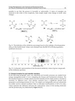
The unit cell of Cu
2
O with a lattice constant of 0.427 nm is composed of a body centered
cubic lattice of oxygen ions, in which each oxygen ion occupies the center of a tetrahedron
formed by copper ions (Xue & Dieckmann, 1990). The Cu atoms arrange in a fcc sublattice,
the O atoms in a bcc sublattice. The unit cell contains 4 Cu atoms and 2 O atoms. One
sublattice is shifted by a quarter of the body diagonal. The space group is Pn3m, which
includes the point group with full octahedral symmetry. This means particularly that parity
is a good quantum number. Figure 1 shows the crystal lattice of Cu
2
O. Molar mass of Cu
2
O
is 143.09 g/mol, density is 6.0 g/cm
3
and its melting and boiling points are 1235°C and
1800°C, respectively. Also, it is soluble in acid and insoluble in water.
Cuprous oxide (copper (I) oxide Cu
2
O) is found in nature as cuprite and formed on copper
by heat. It is a red color crystal used as a pigment and fungicide. Rectifier diodes based on
this material have been used industrially as early as 1924, long before silicon became the
standard. Cupric oxide (copper(II) oxide CuO) is a black crystal. It is used in making fibers
and ceramics, gas analyses and for Welding fluxes. The biological property of copper
compounds takes important role as fungicides in agriculture and biocides in antifouling
paints for ships and wood preservations as an alternative of Tributyltin compounds.
In solar cells, Cu
2
O has not been commonly used because of its low energy conversion
efficiency which results from the fact that the light generated charge carriers in micron-sized
Cu
2
O grains are not efficiently transferred to the surface and lost due to recombination. For
randomly generated charge carriers, the average diffusion time from the bulk to the surface is
given by:
1
Cuprous Oxide as an Active Material for Solar Cells
169
Dr
22
(1)
where r is the grain radius and D is the diffusion coefficient of the carrier (Rothenberger et
al., 1985, as cited in Tang et al., 2005). If the grains radius is reduced from micrometer
dimensions to nanometer dimensions, the opportunities for recombination can be
dramatically reduced. The preparation of nano crystalline Cu
2
O thin films is a key to
improving the performance of solar application devices. Nanotechnologies in this area,
therefore, given their full meaning. In the last decade the scientific literature, abounds with
works again showing progress in research related to obtaining the cuprous oxide.
(
Fig. 1. Crystal structure of Cu
2
O
This chapter presents an overview of recent literature concerning cuprous oxide synthesis
and application as an active material in solar cells, as well as our own results of synthesis
and investigations of Cu
2
O thin films using electrochemical techniques.
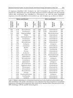
2. Methodologies used for the synthesis of cuprous oxide
The optical and electrical properties of absorber materials in solar cells are key parameters
which determine the performance of solar cells. Hence, it is necessary to tune these
properties properly for high efficient device. Electrical properties of Cu
2
O, such as carrier
mobility, carrier concentration, and resistivity are very dependent on preparation methods.
Cuprous oxide thin films have been prepared by various techniques like thermal oxidation
(Jayatissa et al., 2009; Musa et al., 1998; Sears & Fortin, 1984), chemical vapor deposition
(Kobayashi et al. 2007; Maruyama, 1998; Medina-Valtierra et al., 2002; Ottosson et al., 1995;
Ottosson & Carlsson, 1996), anodic oxidation (Fortin & Masson, 1982; Sears and Fortin, 1984;
Singh et al., 2008), reactive sputtering (Ghosh et al., 2000), electrodeposition (Briskman, 1992;
Daltin et al., 2005; Georgieva & Ristov, 2002; Golden et al., 1996; Liu et al., 2005; Mizuno et
al., 2005; Rakhshani et al., 1987, Rakhshani & Varghese, 1987; Santra et al., 1999; Siripala et
Solar Cells – New Aspects and Solutions
170
al., 1996; Tang et al., 2005; Wang et al., 2007; Wijesundera et al., 2006), plasma evaporation
(Santra et al., 1992), sol–gel-like dip technique (Armelao et al., 2003; Ray, 2001) etc. Each of
these methods has its own advantages and disadvantages. In most of these studies, a
mixture of phases of Cu, CuO and Cu
2
O is generally obtained and this is one of the nagging
problems for non-utilizing Cu
2
O as a semiconductor (Papadimitropoulos et al., 2005). Pure
Cu
2
O films can be obtained by oxidation of copper layers within a range of temperatures
followed by annealing for a small period of time.
Results obtained using different methods, especially thermal oxidation and chemical vapor
evaporation for synthesis of cuprous oxide thin films, are presented in next sections, with
special emphasis on the electrochemical synthesis of cuprous oxide.
2.1 Thermal oxidation
Polycrystalline cuprous oxide can be formed by thermal oxidation of copper under suitable
conditions (Rai, 1988). The procedure involves the oxidation of high purity copper at an
elevated temperature (1000–1500
0
C) for times ranging from few hours to few minutes
depending on the thickness of the starting material (for total oxidation) and the desired
thickness of Cu
2
O (for partial oxidation). Process is followed by high-temperature annealing
for hours or even days.
Sears & Fortin (1984) synthesized cuprous oxide films on copper substrates to a thickness of
a few micrometers, using both thermal and anodic oxidation techniques. The measurements
carried out on the anodic oxide layers indicate an unwanted but inevitable incorporation of
other compounds into the Cu
2
O. They found that the photovoltaic properties of the
resulting Cu
2
O/Cu backwall cells depend critically on the copper surface preparation, as
well as on the specific conditions of oxidation. Backwall cells of the thermal variety with
thicknesses down to 3 μm do not quite yet approach the performance of the best Cu
2
O front
cells, but are much simpler to grow. Serious difficulties with shorting paths in the case of
thermally grown oxide and with the purity of the Cu
2
O in the anodic case will have to be
solved before a solar cell with an oxide layer thickness in the 1.5 to 2 μm range can be
produced.
Musa et al. (1998) produced the cuprous oxide by thermal oxidation and studied its physical
and electrical properties. The oxidation was carried out at atmospheric pressure in a high-
temperature tube furnace. During this process the copper foils were heated in the range of
200 to 1050°C. Cu
2
O has been identified to be stable at limited ranges of temperature and
oxygen pressure. It has also been indicated that during oxidation, Cu
2
O is formed first, and
after a sufficiently long oxidation time CuO is formed (Roos & Karlson, 1983, as cited Musa
et al., 1998). It has been suggested that the probable reactions that could account for the
presence of CuO in layers oxidised below 1000
°C are:
2Cu
2
O + O
2
→ 4CuO (2)
Cu
2
O → CuO + Cu (3)
The unwanted CuO can be removed using an etching solution
consisting of FeCl, HCl, and 8
M HNO
3
containing NaCl. The results of the oxidation process as deduced from both XRD and
SEM studies indicate that the oxide layers resulting from oxidation at 1050
0
C consist entirely of
Cu
2
O. Those grown below 1040
0
C gave mixed oxides of Cu
2
O and CuO. It was observed that
in general the lower the temperature of oxidation, the lower the amount of Cu
2
O was present
in the oxide. Thermodynamic considerations indicate that the limiting temperature for the
Cuprous Oxide as an Active Material for Solar Cells
171
elimination of CuO from the oxide layer was found to be 1040
0
C. For thermal oxidation carried
out below 1040
0
C, Cu
2
O is formed first and it is then gradually oxidised to CuO depending on
the temperature and time of reaction. Pure unannealed Cu
2
O layers grown thermally in air are
observed to exhibit higher resistivity and low hole mobility. A significant reduction in
resistivity and an increase in mobility values were obtained by oxidizing the samples in the
presence of HCl vapour, followed by annealing at 500
0
C. Cu
2
O layers grown in air without the
annealing process gave resistivities in the range 2x10
3
– 3x10
3
Ωcm. A substantial reduction in
the resistivity of the samples was achieved by doping with chlorine during growth and
annealing. An average mobility of 75 cm
2
V
-1
s
-1
at room temperature was obtained for eight
unannealed Cu
2
O samples. This average value increased to 130 cm
2
V
-1
s
-1
after doping the
samples with chlorine and annealing. The SEM studies indicate that the annealing process
results in dense polycrystalline Cu
2
O layers of increased grain sizes which are appropriate for
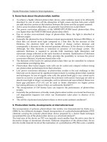
solar-cell fabrication. Figure 2 presents the micrograph of the surface morphology of a copper
foil partially oxidised at 970
0
C for 2 min. The sample was neither annealed nor etched. The
surface shows the black CuO coat formed on the violet-red Cu
2
O after the oxidation process.
The surface morphology is porous and amorphous in nature. The structure formed by this
oxidation process is of the form CuO/Cu
2
O/Cu/Cu
2
O/CuO.
Jayatissa et al. (2009) prepared cuprous oxide (Cu
2
O) and cupric oxide (CuO) thin films by
thermal oxidation of copper films coated on indium tin oxide (ITO) glass and non-alkaline
glass substrates. The formation of Cu
2
O and CuO was controlled by varying oxidation
conditions such as oxygen partial pressure, heat treatment temperature and oxidation time.
Authors used X-ray diffraction, atomic force microscopy and optical spectroscopy to
determinate the microstructure, crystal direction, and optical properties of copper oxide
films. The experimental results suggest that the thermal oxidation method can be employed
to fabricate device quality Cu
2
O and CuO films that are up to 200–300 nm thick.
Fig. 2. SEM micrograph of unetched and unannealed sample oxidised at 970
0
C for 2 min
showing CuO coating (Musa et al., 1998)
Solar Cells – New Aspects and Solutions
172
2.2 Chemical vapor deposition
Chemical vapor deposition is a chemical process used to produce high-purity, high-
performance solid materials. The films may be epitaxial, polycrystalline or amorphous
depending on the materials and reactor conditions. Chemical vapor deposition has become
the major method of film deposition for the semiconductor industry due to its high
throughput, high purity, and low cost of operation. Several important factors affect the
quality of the film deposited by chemical vapor deposition such as the deposition
temperature, the properties of the precursor, the process pressure, the substrate, the carrier
gas flow rate and the chamber geometry.
Maruyama (1998) prepared polycrystalline copper oxide thin films at a reaction temperature
above 280
0
C by an atmospheric-pressure chemical vapor deposition method. Copper oxide
films were grown by thermal decomposition of the source material with simultaneous
reaction with oxygen. At a reaction temperature above 280
0
C, polycrystalline copper oxide
films were formed on the borosilicate glass substrates. Two kinds of films, i.e., Cu
2
O and
CuO, were obtained by adjusting the oxygen partial pressure. Also, there are large
differences in color and surface morphology between the CuO and Cu
2
O films obtained.
Author found that the surface morphology and the color of CuO film change with reaction
temperature. The CuO film prepared at 300
0
C is real black, and the film prepared at 500
0
C is
grayish black.
Medina-Valtierra et al. (2002) coated fiber glass with copper oxides, particularly in the form
of 6CuO•Cu
2
O by chemical vapor deposition method. The authors’ work is based on design
of an experimental procedure for obtaining different copper phases on commercial
fiberglass. Films composed of copper oxides were deposited over fiberglass by sublimation
and transportation of (acac)
2
Cu(II) with a O
2
flow (oxidizing agent), resulting in the
decomposition of the copper precursor, deposition of Cu
0
and Cu
0
oxidation on the
fiberglass over a short range of deposition temperatures. The copper oxide films on the
fiberglass were examined using several techniques such as X-ray diffraction (XRD), visible
spectrophotometry, scanning electronic microscopy (SEM) and atomic force microscopy
(AFM). The films formed on fiberglass showed three different colors: light brown, dark
brown and gray when Cu
2
O, 6CuO•Cu
2
O or CuO, respectively, were present. At a
temperature of 320°C only cuprous oxide is formed but at a higher temperature of about
340°C cupric oxide is formed. At a temperature of 325°C 6CuO-Cu
2
O is formed. The
decomposition of precursor results in the formation of a zero valent copper which upon
oxidation at different temperature gives different oxides.
Ottosson et al. (1995) deposited thin films of Cu
2
O onto MgO (100) substrates by chemical
vapour deposition from copper iodide (CuI) and dinitrogen oxide (N
2
O) at two deposition
temperatures, 650°C and 700°C. They found that the pre-treatment of the substrate as well
as the deposition temperature had a strong influence on the orientation of the nuclei and the
film. For films deposited at 650°C several epitaxial orientations were observed: (100), (110)
and (111). The Cu
2
O(100) was found to grow on a defect MgO(100) surface. When the
substrates were annealed at 800°C in N
2
O for 1 h, the defects in the surface disappeared and
only the (110) orientation was developed during the deposition. The films deposited at
700°C (without annealing of the substrates) displayed only the (110) orientation.
Markworth et al. (2001) prepared cuprous oxide (Cu
2
O) films on single-crystal MgO(110)
substrates by a chemical vapor deposition process in the temperature range 690–790°C.
Cu
2
O (a=0.4270 nm) and MgO (a=0.4213 nm) have cubic crystal structures, and the lattice
mismatch between them is 1.4%. Due to good lattice match, chemical stability, and low cost,
Cuprous Oxide as an Active Material for Solar Cells
173
MgO single crystals are particularly effective substrates for the growth of Cu
2
O thin films.
Authors found that the Cu
2
O films grow by an island-formation mechanism on MgO
substrate. Films grown at 690°C uniformly coat the substrate except for micropores between
grains. However, at a growth temperature of 790°C, an isolated, three-dimensional island
morphology develops.
Kobayashi et al. (2007) investigated the high-quality Cu
2
O thin films grown epitaxially on
MgO (110) substrate by halide chemical vapor deposition under atmospheric pressure. CuI
in a source boat was evaporated at a temperature of 883 K, and supplied to the growth zone
of the reactor by N
2
carrier gas, and O
2
was also supplied there by the same carrier gas.
Partial pressure of CuI and O
2
were adjusted independently to 1.24 x 10
−2
and 1.25 x 10
3
Pa.
They found that the optical band gap energy of Cu
2
O film calculated from absorption
spectra is 2.38 eV. The reaction of CuI and O
2
under atmospheric pressure yields high-
quality Cu
2
O films.
2.3 Other methods
Several novel methods for the synthesis of cuprous oxide (i.e. reactive sputtering, sol-gel
technique, plasma evaporation,) and some results obtained using these techniques are
presented in this part. For example, Santra et al. (1992) deposited thin films of cuprous oxide
on the substrates by evaporating metallic copper through a plasma discharge in the
presence of a constant oxygen pressure. Authors found two oxide phases before and after
annealing treatment of films. Before annealing treatment, cuprous oxide was identified and
after annealing in a nitrogen atmosphere, cuprous oxide changes to cupric oxide. The results
of optical absorption measurement show that the band gap energies for Cu
2
O and CuO are
2.1 eV and 1.85 eV, respectively. Thin films prepared in the absence of a reactive gas and
plasma were also deposited on glass substrates and in these films the presence of metallic
copper was identified.
Ghosh et al. (2000) deposited cuprous oxide and cupric oxide by RF reactive sputtering at
different substrate temperatures, namely, at 30, 150 and 300
0
C. They used atomic force
microscopy for examination of the properties of the prepared oxides films related to surface
morphology. It was found for the film deposited at 30
0
C, that, 8-10 small grains of size ~40
nm diameter agglomerate together and make a big grain of size ~120 nm. At the
temperature of 150
0
C the grain size becomes 160 nm. The grain size decreases to 90 nm at
300
0
C. From thickness and deposition time, the deposition rates of the films are found to be
8, 11.5 and 14.0 nm/min for substrate temperature corresponding to 30, 150 and 300
0
C,
respectively. Optical band gap of the films deposited at 30, 150 and 300
0
C are 1.75, 2.04 and
1.47 eV, respectively. Different phases of copper oxides are found at different temperatures
of deposition. CuO phase is obtained in the films prepared at a substrate temperature of
300
0
C.
Sol gel-like dip technique is a very simple and low-cost method, which requires no
sophisticated specialized setup. For example, Armelao et al. (2003) used a sol-gel method
to synthesize nanophasic copper oxide thin films on silica slides. They used copper acetate
monohydrate as a precursor in ethanol as a solvent. Authors observed formation of CuO
crystallites in the samples annealed under inert atmosphere (N
2
) up to 3 h. A prolonged
treatment (5 h) in the same environment resulted in the complete disappearance of
tenorite and in the formation of a pure cuprite crystalline phase. Also, under reducing
conditions, the formation of CuO, Cu
2
O and Cu was progressively observed, leading to a
mixture of Cu(II) and Cu(I) oxides and metallic copper after treatment at 900
0
C for 5 h.
Solar Cells – New Aspects and Solutions
174
All the obtained films have nanostructure with an average crystallite size lower than
20 nm.
Nair et al. (1999) deposited cuprous oxide thin films on glass substrate using chemical
technique. The glass slides were dipped first in a 1 M aqueous solution of NaOH at the
temperature range 50-90°C for 20 s and then in a 1 M aqueous solution of copper complex.
X-ray diffraction patterns showed that the films, as prepared, are of cuprite structure with
composition Cu
2
O. Annealing the films in air at 350
0
C converts these films to CuO. This
conversion is accompanied by a shift in the optical band gap from 2.1 eV (direct) to 1.75
eV (direct). The films show p-type conductivity, ~ 5 x 10
-4
Ω
-1
cm
-1
for a film of thickness
0.15 μm.
3. Electrochemical synthesis
3.1 Electrodeposition
Synthesis of Cu
2
O nanostructures by the methods described in the previous part demands
complex process control, high reaction temperatures, long reaction times, expensive
chemicals and specific method for specific nanostructures. A request for obtaining
nanometer particles, cause complete change of technology in which Cu
2
O is formed on the
cathode by reduction of Cu
2+
ions from the organic electrolyte. The possible reactions during
the cathodic reduction of copper (II) lactate solution are:
2Cu
2+
+ H
2
O + 2e
= Cu
2
O + 2H
+
(4)
Cu
2+
+ 2e
= Cu (5)
Cu
2
O + 2H
+
+ 2e
= 2Cu + H
2
O (6)
The electrodeposition techniques are particularly well suited for the deposition of single
elements but it is also possible to carry out simultaneous depositions of several elements
and syntheses of well-defined alternating layers of metals and oxides with thicknesses
down to a few nm. So, electrodeposition is a suitable method for the synthesis of
semiconductor thin films such as oxides. This method provides a simple way to deposit
thin Cu(I) oxide films onto large-area conducting substrates (Lincot, 2005). Thus, the
study of the growth kinetics of these films is of considerable importance. In this section
we present some results of electrochemical deposition of cuprous oxide obtained by
various authors.
Rakhshani et al. (1987) cathodically electrodeposited Cu(I) oxide film onto conductive
substrates from a solution of cupric sulphate, sodium hydroxide and lactic acid. Films of
Cu
2
O were deposited in three different modes, namely the potentiostatic mode, the mode
with constant WE potential with respect to the CE and the galvanostatic mode. The
composition of the films deposited under all conditions was Cu
2
O with no traces of CuO.
The optical band gap for electrodeposited Cu
2
O films was 1.95 eV. Deposition
temperature played an important role in the size of deposited grains. Films were
photoconductive with high dark resistivities. Also, Rakhshani & Varghese (1987)
electrodeposited cuprous oxide thin films galvanostatically on 0.05 mm thick stainless
steel substrates at a temperature of 60
0
C. The deposition solution with pH 9 consisted of
lactic acid (2.7 M), anhydrous cupric sulphate (0.4 M), and sodium hydroxide (4 M).
Authors found that all the films deposited at 60 °C consisted only of Cu
2
O grains a few
Cuprous Oxide as an Active Material for Solar Cells
175
μm in size and preferentially oriented along (100) planes parallel to the substrate surface.
A band gap was found and it was 1.90-1.95 eV.
Mukhopadhyay et al. (1992) deposited Cu
2
O films by galvanostatic method on copper
substrates. An alkaline cupric sulphate (about 0.3 M) bath containing NaOH (about 3.2 M)
and lactic acid (about 2.3 M) was used as the electrolyte at pH 9. The bath temperatures
were 40, 50 and 60°C. XRD analysis indicated a preferred (200) orientation of the Cu
2
O
deposited film. The deposition kinetics was found to be independent of deposition
temperature and linear in the thickness range studied (up to about 20 μm). The electrical
conductivity of Cu
2
O films was found to vary exponentially with temperature in the 145-
300
0
C range with associated activation energy of 0.79 eV.
Golden et al. (1996) found that the reflectance and transmittance of the electrodeposited
films of cuprous oxide give a direct band gap of 2.1 eV. Namely, authors used
electrodeposition method for obtaining the films of cuprous oxide by reduction of copper
(II) lactate in alkaline solution (0.4 M cupric sulfate and 3 M lactic acid). Films were
deposited onto either stainless steel or indium tin oxide (ITO) substrates. Deposition
temperatures ranged from 25 to 65 °C. They found that the cathodic deposition current was
limited by a Schottky-like barrier that forms between the Cu
2
O and the deposition solution.
A barrier height of 0.6 eV was determined from the exponential dependence of the
deposition current on the solution temperature. At a solution pH 9 the orientation of the
film is [100], while at a solution pH 12 the orientation changes to [111]. The degree of [111]
texture for the films grown at pH 12 increased with applied current density.
Siripala et al. (1996) deposited cuprous oxide films on indium tin oxide (ITO) coated glass
substrates in a solution of 0.1 M sodium acetate and 1.6 x 10
-2
M cupric acetate and the effect
of annealing in air has been studied too. Electrodeposition was carried out for 1.5 h in order
to obtain films of thicknesses in the order of 1 μm. Authors concluded that the
electrodeposited Cu
2
O films are polycrystalline with grain sizes in the order of 1-2 μm and
the bulk crystal structure is simple cubic. They concluded that there is no apparent change
in the crystal structure when heat treated in air at or below 300°C. Annealing in air changes
the morphology of the surface creating a porous nature with ring shaped structures on the
surface. Annealing above 300°C causes decomposition of the yellow-orange colour Cu
2
O
film into a darker film containing black CuO and its complexes with water.
Zhou & Switzer (1998) deposited Cu
2
O films on stainless steel disks by the cathodic
reduction of copper (II) lactate solution (0.4 M cupric sulfate and 3 M lactic acid). The pH of
the bath was between 7 and 12 and the bath temperature was 60°C. Authors concluded that
the preferred orientation and crystal shape of Cu
2
O films change with the bath pH and the
applied potential. They obtained pure Cu
2
O films at bath pH 9 with applied potential
between -0.35 and -0.55 (SCE) or at bath pH 12.
Mahalingam et al. (2000) deposited cuprous oxide thin films on copper and tin-oxide-coated
glass substrates by cathodic reduction of alkaline cupric lactate solution (0.45 M CuSO
4
, 3.25
M lactic acid and 0.1 M NaOH). The deposition was carried out in the temperature range of
60-80
0
C at pH 9. Galvanostatic deposition on tin-oxide-coated glass and copper substrates
yields reddish-grey Cu
2
O films. All the films deposited are found to be polycrystalline
having grains in the range of 0.01 - 0.04 μm. The deposition kinetics is found to be linear and
independent of the deposition temperature. From the optical absorption measurements,
authors found that the deposit of cuprous oxide films has a refractive index of 2.73, direct
band gap of 1.99 eV, and extinction coefficient of 0.195. After deposition on temperature of
70
0
C, cuprous oxide films were annealed in air for 30 min at different temperatures (150, 250
Solar Cells – New Aspects and Solutions
176
and 350
0
C) to obtain their room temperature resistivity. It showed a decrease in resistivity of
Cu
2
O film of the order of 10
7
Ωcm to 10
4
Ωcm. The explanation of such behavior may be due
to increase in hole conduction.
Georgieva & Ristov (2002) deposited the cuprous oxide (Cu
2
O) films using a galvanostatic
method from an alkaline CuSO
4
bath containing lactic acid and sodium hydroxide (64 g/l
anhydrous cupric sulphate (CuSO
4
), 200 ml/l lactic acid (C
3
H
6
O
3
) and about 125 g/l sodium
hydroxide (NaOH)). The electrodeposition temperature was 60
0
C. Authors obtained
polycrystalline films of 4–6 μm in thickness with optical band gap of 2.38 eV.
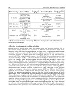
Daltin et al. (2005) applied potentiostatic deposition method to obtain cuprous oxide
nanowires in polycarbonate membrane by cathodic reduction of alkaline cupric lactate
solution (0.45 M Cu(II) and 3.25 M lactate). Authors found that the optimum electrochemical
parameters for the deposition of nanowires are: pH 9.1, temperature 70
0
C, and applied
potential -0.9 V (SSE). The morphology of the nanowires was analyzed by SEM. The obtained
nanowires had uniform diameters of about 100 nm and lengths up to 16 μm. Scanning electron
micrograph of electrodeposited Cu
2
O nanowires are presented in Figure 3.
Liu et al. (2005) investigated the electrochemical deposition of Cu
2
O films onto three
different substrates (indium tin oxide film coated glass, n-Si wafer with (001) orientation and
Au film evaporated onto Si substrate). For the film grown on ITO, electrical current
increases gradually during deposition, while for the films growth on both Si and Au
substrates, the monitored current decreases monotonically. Authors considered that the
continuous decrease in current reflects different deposition mechanisms. In the case of Si
substrate, the decrease of the current may be the result of the formation of an amorphous
SiO
2
layer on the Si surface, which limits the current. For the Au surface, the decrease in
measured current is due to the resistivity increase as a result of Cu
2
O film formation. Cu
2
O
crystals with microsized pyramidal shape were grown on ITO substrate. Nanosized and
pyramidal shaped Cu
2
O particles were formed on Si substrate and the film grown on Au
substrate shows a (100) orientation with much better crystallinity.
Fig. 3. (a) Scanning electron micrograph of electrodeposited Cu
2
O nanowires. Bath
temperature 70
0
C, pH 9.1, E -1.69 V/
SSE
. (b) Enlarged (a) (Daltin et al., 2005)
Cuprous Oxide as an Active Material for Solar Cells
177
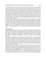
Tang et al. (2005) investigated the electrochemical deposition of nanocrystalline Cu
2
O thin
films on TiO
2
films coated on transparent conducting optically (TCO) glass substrates by
cathodic reduction of cupric acetate (0.1 M sodium acetate and 0.02 M cupric acetate). Authors
concluded that the pH and bath temperature strongly affect the composition and
microstructure of the Cu
2
O thin films. The effect of bath pH on electrodeposition of Cu
2
O thin
film was investigated by selecting a bath temperature of 30
0
C and an applied potential of -245
mV (SCE). Authors found that the films deposited at pH 4 are mostly metallic Cu and only
little Cu
2
O. In the region of pH 4 to pH 5.5, the deposited films are a composite of Cu and
Cu
2
O, while the films deposited at pH between 5.5 and 6 are pure Cu
2
O. Pure Cu
2
O deposited
at bath temperature between 0 and 30
0
C produced spherically shaped grains with 40~50 nm in
diameter. The bath temperature must be controlled in the range of 0-30
0
C to obtain
nanocrystalline Cu
2
O thin film. At a temperature of 45°C, a highly branched dendrite formed,
and the grain size increased to 200–500 nm. At the temperature above 60°C, a ring-shaped
structure with a porous surface was observed. Optical absorption measurements indicate that
annealing at 200
0
C can improve the transmittance of the nanocrystalline Cu
2
O thin films.
Figure 4 shows SEM photographs of Cu
2
O films deposited at various bath temperatures.
Fig. 4. SEM photographs of Cu
2
O films deposited at various bath temperatures: (A) 0
0
C, (B)
30
0
C, (C) 45
0
C, and (D) 60
0
C (Tang et al., 2005)
Wijesundera et al. (2006) investigated the potentiostatic electrodeposition of cuprous oxide
and copper thin films. Electrodeposition was carried out in an aqueous solution containing
Solar Cells – New Aspects and Solutions
178
sodium acetate and cupric acetate. The results of their investigation show that the single
phase polycrystalline Cu
2
O can be deposited from 0 to -300 mV (SCE). Also, co-deposition of
Cu and Cu
2
O starts at - 400 mV (SCE). At the deposition potential from -700 mV (SCE) a
single phase Cu thin films are produced. Single phase polycrystalline Cu
2
O thin films with
cubic grains of 1–2 μm can be possible at the deposition potential around -200 mV (SCE).
Wang et al. (2007) cathodically electrodeposited cuprous oxide films from 0.4 M copper
sulfate bath containing 3 M lactic acid. The bath pH was carefully adjusted between 7.5 and
12.0 by controlled addition of 4 M NaOH. The electrodeposition was done on Sn-doped
indium oxide substrates. The influence of electrodeposition bath pH on grain orientation
and crystallite shape was examinated. Authors found that three orientations, namely, (100),
(110), and (111) dominate as the bath pH is increased from ~ 7.5 to ~ 12.
Recently, Hu et al. (2009) electrodeposited Cu
2
O thin films onto an indium tin oxide (ITO)
coated glass by a two-electrode system with acid and alkaline electrolytes under different
values of direct current densities. Copper foils were used as the anodes, and the current
density between the anode and cathode varied between 1 mA cm
−2
and 5 mA cm
−2
. It was
obtained that the microstructure of Cu
2
O thin films produced in the acid electrolyte changes
from a ring shape to a cubic shape with the increase of direct current densities. The
microstructure of Cu
2
O thin films produced in the alkaline electrolyte has a typical pyramid
shape. The electrocrystallization mechanisms are considered to be related to the nucleation
rate, cluster growth, and crystal growth. To investigate the initial stage of nucleation and
cluster growth, different current densities with the same deposition time were applied.
Figure 5 shows that a relatively large cluster size and a relatively small number of
nucleation sites were obtained under a current density of 1 mAcm
−2
. At a high current
density of 5 mAcm
−2
, more nucleation sites and a small cluster size were obtained.
Fig. 5. The Cu
2
O films synthesized under different current densities with the same
deposition time (Hu et al., 2009)
Cuprous Oxide as an Active Material for Solar Cells
179
Fig. 6. Current density vs. time curves for electrodeposition of Cu
2
O thin film on titanium
electrode (electrodeposition time: (A ) 6 s, (B) 10 s and (C) 60 s; t = 25 ºC, pH 9.22)
Solar Cells – New Aspects and Solutions
180
Bugarinović et al. (2009) investigated the electrochemical deposition of thin films of cuprous
oxide on three different substrates (stainless steel, platinum and copper). All experiments of
Cu
2
O thin films deposition were performed at room temperature. Using experimental
technique described elsewhere (Stević & Rajčić-Vujasinović, 2006; Stević & et al., 2009),
electrodeposition was carried out in in a copper lactate solution as an organic electrolyte (0.4
M copper sulfate and 3 M lactic acid, pH 7-10 is set using NaOH). The conditions are
adjusted so that the potentials which arise Cu
2
O and CuO are as different as possible.
Characterization of obtained coatings was performed by cyclic voltammetry. The results
indicate that the composition of the substrate strongly affects electrochemical reactions.
Reaction with the highest rate took place on a copper surface, while the lowest rate was
obtained on the platinum electrode. The results show that the co-deposit of Cu
2
O and Cu
was obtained at - 800 mV (SCE) on stainless steel electrode. The same authors investigated
the electrodeposition of cuprous oxide thin film on titanium electrode. The obtained results
are presented in Figure 6.
Cuprous oxide thin films were deposited at potentials -0.6 V, -0.8 V, -1.0 V and 1.2 V with
respect to SCE. All experiments were carried out for a duration of 6 s, 10 s and 1 minute.
When the electrodeposition lasted 6 s (Fig. 6A), obtained currents depended on applied
potentials. Lowest current of 1mA was obtained at the potential of -0.6 V vs. SCE, while the
highest value of 17.9 mA was reached at -1.2 V (SCE). When the electrodeposition time was
10 s (Fig. 6B), curves current vs. time had similar shape as the previous, but when the
process duration prolongates to 60 s (Fig. 6C), currents obtained at higher potentials (-1.0 V
and -1.2 V vs. SCE) decrease after about 15 s and stabilise again after about 40 s at some
lower value (nearly 80% of the previous ones). Maximum theoretical thicknesses of Cu
2
O
film for every applied potential and all process durations were calculated. The lowest
thickness of 7 nm was obtained for 6 s with potential of -0.6 V (SCE). More negative
potentials and the increase of time lead to the increase of the film thickness. Theoretical
value of the Cu
2
O film thickness for the longest time (60 s) and most negative potential
(-1.2 V vs. SCE) is about 900 nm.
3.2 Anodic oxidation
In spite of the simple equipment and easy process control, cathodic synthesis demands
expensive chemicals as a big dissadventage. On the other hand, anodic oxidation of copper
in alkaline solution is one of the standard methodologies for producing cuprous oxide
powders used for marine paints and for plants preservation. Those powders are composed
of particles of micrometer scale. However, solar sells, for their part, require particles or films
of much smaller dimensions in order to achieve higher efficiency. Passive protecting layers
formed on copper during anodic oxidation in alkaline solutions are widely investigated and
described in electrochemical literature. The structure of those films formed on copper in
neutral and alkaline solutions consists mainly of Cu
2
O and CuO or Cu(OH)
2
. Applying in
situ electrochemical scanning tunneling microscopy (STM), Kunze et al. (2003) found that in
NaOH solutions, a Cu
2
O layer is formed at E > 0.58-0.059 pH (V vs. SHE). A Cu
2
O/Cu(OH)
2
duplex film is found for E > 0.78-0.059 pH (V vs. SHE). In borate buffer solutions, oxidation
to Cu
2
O leads to non-crystalline grain like structure, while a crystalline and epitaxial Cu
2
O
layer has been observed in 0.1 M NaOH indicating a strong anion and/or pH effect on the
crystallinity of the anodic oxide film.
Stanković et al. (1998; 1999) investigated the effect of different parameters such as
temperature, pH and anodic current density on CuO powder preparation. The lowest value
Cuprous Oxide as an Active Material for Solar Cells
181
of average crystallite size was obtained at pH 7.5, whereas the highest value was obtained at
pH 9.62. They found a strong dependence of grain size and cupric oxide purity on current
density. The average srystallite size increased from 45 nm (at a current density of 500 Am
-2
)
to 400 nm (at a current density of 4000 Am
-2
), other conditions being as follows: pH 7.5,
temperature of 353 K and 1.5 M Na
2
SO
4
.
There have been a number of papers on anodic formation of thin Cu
2
O layers (< 1 m) using
alkaline solutions, but some work has been done with slightly acidic solutions. For example,
backwall Cu
2
O/Cu photovoltaic cells have been prepared by Sears and Fortin (Sears &
Fortin, 1983) with the Cu
2
O layer being about 1 m thick. They used and compared two
methods of oxidation – thermal and anodic. The condition of the underlying copper surface
is expected to influence the resulting parameters of thin solar cells, so they examined the
influence of the surface preparation of the starting copper (i.e., polishing technique, thermal
annealing). All this experience can help in researching the optimal way of production of
nanostructured Cu
2
O powders or films.
Recently, Singh et al. (2008) reported synthesis of nanostructured Cu
2
O by anodic oxidation
of copper through a simple electrolysis process employing plain water as electrolyte. They
found two different types of Cu
2
O nanostructures. One of them belonged to particles
collected from the bottom of the electrolytic cell, while the other type was located on the
copper anode itself. The Cu
2
O structures collected from the bottom consist of nanowires
(length, ~ 600–1000 nm and diameter, ~ 10–25 nm). It may be mentioned that the total length
of Cu
2
O nanothread and nanowire is comprised of several segments. These were
presumably formed due to interaction between nanothreads/nanowires forming the
network in which the Cu
2
O nanothread/nanowire configuration finally appears. When the
electrolysis conditions were maintained at 10 V for 1 h, the representative TEM
microstructure revealed the presence of dense Cu
2
O nanowire network (length, ~ 1000 nm,
diameter, ~ 10–25 nm). The X-ray diffraction pattern obtained from these nanomaterials,
could be indexed to a cubic system with lattice parameter, a = 0.4269 ± 0.005 nm. These tally
quite well with the lattice parameter of Cu
2
O showing that the material formed under
electrolysis conditions consists of cubic Cu
2
O lattice structure.
In addition to the delaminated nanostructures, investigations of the copper anode, which
were subjected to electrolysis runs, revealed the presence of another type of nanostructure of
Cu
2
O. Authors propose that the higher applied voltage (e.g. 8 V or 10 V) for electrolysis
represents the optimum conditions for the formation of nanocubes. These nanocubes reflect
the basic cubic unit cell of Cu
2
O.
4. Conclusion
Copper oxides, especially cuprous oxide, are of interest because of their applications in
solar cell technology. The semiconductor cuprous oxide Cu
2
O film has been of
considerable interest as a component of solar cells due to its band gap energy and high
optical absorption coefficient. Since the properties of cuprous oxide not only depend upon
the nature of the material but also upon the way they are synthesized, different methods
and results obtained on the synthesis of cuprous oxide by various researchers are
discussed in this chapter. The properties of the prepared cuprous oxide films related to
surface morphology are presented too. In this chapter, the point is made on
electrodeposition of cuprous oxide because electrodeposition techniques are particularly
well suited for the deposition of metal oxides with thicknesses down to a few nm. The
Solar Cells – New Aspects and Solutions
182
results obtained show that the cuprous oxide can be used as a potential active material for
solar cells application.
5. Acknowledgment
This work was supported by Ministry of Science and Technological Development of
Republic of Serbia, Project No. OI 172 060.
6. References
Akimoto, K.; Ishizuka, S.; Yanagita, M.; Nawa, Y.; Paul, G. K. & Sakurai, T. (2006). Thin Film
Deposition of Cu
2
O and Application for Solar Cells. Solar Energy, Vol. 80, No.6,
(June 2006), pp. 715–722, ISSN 0038-092X
Armelao, L.; Barreca, D.; Bertapelle, M.; Bottaro, G.; Sada, C. & Tondello, E. (2003). A Sol–gel
Approach to Nanophasic Copper Oxide Thin Films. Thin Solid Films, Vol.442, No.1-
2, (October 2003), pp. 48–52, ISSN 0040-6090
Briskman, R.N. (1992). A Study of Electrodeposited Cuprous Oxide Photovoltaic Cells. Solar
Energy Materials and Solar Cells, Vol.27, No.4, (September 1992), pp. 361–368, ISSN
0927-0248
Bugarinović, S.J.; Grekulović, V.J.; Rajčić-Vujasinović, M.M.; Stević, Z.M. & Stanković, Z.D.
(2009). Electrochemical Synthesis and Characterization of Copper(I) Oxide (in
Serbian). Hemijska Industrija, Vol.63, No.3, (May-June 2009), pp. 201-207, ISSN 0367-
598X
Daltin, A-L.; Addad, A. & Chopart, J-P. (2005). Potentiostatic Deposition and
Characterization of Cuprous Oxide Films and Nanowires. Journal of Crystal Growth,
Vol.282, No.3-4, (September 2005), pp. 414-420, ISSN 0022-0248
Fortin, E. & Masson, D. (1982). Photovoltaic Effects in Cu
2
O-Cu Solar Cells Grown by
Anodic Oxidation. Solid-State Electronics, Vol.25, No.4, (April 1982), pp. 281-283,
ISSN 0038-1101
Georgieva, V. & Ristov, M. (2002). Electrodeposited Cuprous Oxide on Indium Tin Oxide
for Solar Applications. Solar Energy Materials and Solar Cells, Vol.73, No.1, (May
2002), pp. 67–73, ISSN 0927-0248
Ghosh, S.; Avasthi, D.K.; Shah, P.; Ganesan, V.; Gupta, A.; Sarangi, D.; Bhattacharya, R. &
Assmann, W. (2000). Deposition of Thin Films of Different Oxides of Copper by RF
Reactive Sputtering and Their Characterization. Vacuum, Vol.57, No.4, (June 2000),
pp. 377-385, ISSN 0042-207X
Golden, T.D.; Shumsky, M.G.; Zhou, Y.; Vander Werf, R.A.; Van Leeuwen, R.A. & Switzer,
J.A. (1996). Electrochemical Deposition of Copper (I) Oxide Films. Chemistry of
Materials, Vol. 8, No.10, (October 1996), pp. 2499–2504, ISSN 0897-4756
Grozdanov, I. (1994). Electroless Chemical Deposition Technique for Cu
2
O Thin Films.
Materials Letters, Vol.19, No.5-6, (May 1994), pp. 281–285, ISSN 0167-577X
Han, K. & Tao, M. (2009). Electrochemically Deposited p–n Homojunction Cuprous Oxide
Solar Cells. Solar Energy Materials and Solar Cells, Vol. 93, No.1, (January 2009),
pp.153-157, ISSN 0927-0248
Hu, F.; Chan, K.C. & Yue, T.M. (2009). Morphology and Growth of Electrodeposited
Cuprous Oxide under Different Values of Direct Current Density. Thin Solid Films,
Vol. 518, No.1, (November 2009), pp. 120–125, ISSN 0040-6090
Cuprous Oxide as an Active Material for Solar Cells
183
Jayatissa, A.H.; Guo, K. & Jayasuriya, A.C. (2009). Fabrication of Cuprous and Cupric Oxide
Thin Films by Heat Treatment. Applied Surface Science, Vol.255, No.23, (September
2009), pp. 9474-9479, ISSN 0169-4332
Kobayashi, H.; Nakamura , T. & Takahash, N. (2007). Preparation of Cu
2
O Films on MgO
(110) Substrate by Means of Halide Chemical Vapor Deposition under Atmospheric
Pressure. Materials Chemistry and Physics, Vol.106, No.2-3, (December 2007), pp. 292-
295, ISSN 0254-0584
Kunze, J.; Maurice, V.; Klein, L.H.; Strehblow, H.H. & Marcus, P. (2003). In Situ STM Study
of the Effect of Chlorides on the Initial Stages of Anodic Oxidation of Cu(111) in
Alkaline Solutions. Electrochimica Acta, Vol.48, No.9, (April 2003), pp.1157-1167,
ISSN 0013-4686
Lee, Y.H.; Leu, I.C.; Chang, S.T.; Liao, C.L. & Fung, K.Z. (2004). The Electrochemical
Capacities and Cycle Retention of Electrochemically Deposited Cu
2
O Thin Film
Toward Lithium. Electrochimica Acta, Vol.50, No.2-3, (November 2004), pp. 553–559,
ISSN 0013-4686
Lincot, D. (2005). Electrodeposition of semiconductors. Thin Solid Films, Vol. 487, No.1-2,
(September 2005), pp. 40–48, ISSN 0040-6090
Liu, Y.L.; Liu, Y.C.; Mu, R.; Yang, H.; Shao, C.L.; Zhang, J.Y.; Lu, Y.M.; Shen, D.Z. & Fan,
X.W. (2005). The Structural and Optical Properties of Cu
2
O Films Electrodeposited
on Different Substrates. Semiconductor Science and Technology, Vol.20, No.1, pp. 44-
49, (January 2005), ISSN 0268-1242
Mahalingam, T.; Chitra, J.S.P.; Rajendran, S.; Jayachandran, M. & Chockalingam, M.J. (2000).
Galvanostatic deposition and characterization of cuprous oxide thin films. Journal of
Crystal Growth, Vol. 216, No.1-4, (June 2000), pp. 304–310, ISSN 0022-0248
Markworth, P.R.; Liu, X.; Dai, J.Y.; Fan, W.; Marks, T.J. & Chang, R.P.H. (2001). Coherent
Island Formation of Cu
2
O Films Grown by Chemical Vapor Deposition on MgO
(110). Journal of Materials Research, Vol.16, No.8, (August 2001), pp. 2408-2414, ISSN
0884-2914
Maruyama, T. (1998). Copper Oxide Thin Films Prepared from Copper
Dipivaloylmethanate and Oxygen by Chemical Vapor Deposition. Japanese Journal
of Applied Physics, Vol. 37, No.7A, pp. 4099-4102, ISSN 0021-4922
Medina-Valtierra, J.; Ramırez-Ortiz, J.; Arroyo-Rojas, V.M.; Bosch, P. & De los Reyes, J.A.
(2002). Chemical Vapor Deposition of 6CuO•Cu
2
O Films on Fiberglass. Thin Solid
Films, Vol. 405, No.1-2, (February 2002), pp. 23–28, ISSN 0040-6090
Mizuno, K.; Izaki, M.; Murase, K.; Shinagawa, T.; Chigane, M.; Inaba, M.; Tasaka, A. &
Awakura, Y. (2005). Structural and Electrical Characterizations of Electrodeposited
p-type Semiconductor Cu
2
O Films. Journal of The Electrochemical Society, Vol.152,
No.4, pp. C179–C182, ISSN 0013-4651
Mukhopadhyay, A.K.; Chakraborty, A.K.; Chatterjee, A.P. & Lahiri, S.K. (1992).
Galvanostatic Deposition and Electrical Characterization of Cuprous Oxide Thin
Films. Thin Solid Films, Vol.209, No.1, (March 1992), pp. 92-96, ISSN 0040-6090
Musa, A.O.; Akomolafe, T. & Carter, M.J. (1998). Production of Cuprous Oxide, a Solar Cell
Material, by Thermal Oxidation and a Study of Its Physical and Electrical
Properties. Solar Energy Materials and Solar Cells, Vol.51, No.3-4, (February 1998), pp.
305-316, ISSN 0927-0248
Solar Cells – New Aspects and Solutions
184
Nair, M.T.S.; Guerrero, L.; Arenas, O.L. & Nair, P.K. (1999). Chemically Deposited Copper
Oxide Thin Films: Structural, Optical and Electrical Characteristics. Applied Surface
Science, Vol.150, No.1-4, (August 1999), pp. 143-151, ISSN 0169-4332
Nozik, A.J. (1978). Photoelectrochemistry: Applications to Solar Energy Conversion. Annual
Review of Physical Chemistry, Vol.29, No.1, (October 1978), pp. 189-222, ISSN 0066-
426X
Ottosson, M.; Lu, J. & Carlsson, J-O. (1995). Chemical Vapour Deposition of Cu
2
O on
MgO(100) from CuI and N
2
0: Aspects of Epitaxy. Journal of Crystal Growth, Vol.151,
No.3-4, (June 1995) pp. 305-311, ISSN 0022-0248
Ottosson, M. & Carlsson, J-O. (1996). Chemical Vapour Deposition of Cu
2
O and CuO from
CuI and O
2
or N
2
O. Surface and Coatings Technology, Vol. 78, No.1-3, (January 1996),
pp. 263-273, ISSN 0257-8972
Papadimitropoulos, G.; Vourdas, N.; Vamvakas, V.Em. & Davazoglou, D. (2005). Deposition
and Characterization of Copper Oxide Thin Films. Journal of Physics: Conference
Series, Vol. 10, No.1, pp. 182–185, ISSN 1742-6588
Pollack, G.P. & Trivich, D. (1975). Photoelectric Properties of Cuprous Oxide. Journal of
Applied Physics, Vol.46, No.1, (January 1975), pp. 163–172, ISSN 0021-8979
Rai, B.P. (1988). Cu
2
O Solar Cells: A Review. Solar Ceils, Vol.25, No.3, (December 1988), pp.
265–272, ISSN 0379-6787
Rajčić-Vujasinović, M.; Stević, Z. & Djordjević, S. (1994). Application of Pulse Potential for
Oxidation of Natural Mineral Covellite (in Russian). Zhurnal prikladnoi khimii
(Russian Journal of Applied Chemistry), Vol.67, No.4, pp. 594-597, ISSN 1070-4272
Rajčić-Vujasinović, M.M.; Stanković, Z.D. & Stević, Z.M. (1999). The Consideration of the
Analogue Electrical Circuit of the Metal or Semiconductor/Electrolyte Interfaces
Based on the Time Transient Analysis. Elektrokhimiya (Russian Journal of
Electrochemistry), Vol.35, No.3, pp. 347-354, ISSN 1023-1935
Rakhshani, A.E.; Al-Jassar, A.A. & Varghese, J. (1987). Electrodeposition and
Characterization of Cuprous Oxide. Thin Solid Films, Vol.148, No.2, (April 1987), pp.
191-201, ISSN 0040-6090
Rakhshani, A.E. & Varghese, J. (1987). Galvanostatic Deposition of Thin Films of Cuprous
Oxide. Solar Energy Materials, Vol.15, No.4, (May-June 1987), pp. 237-248, ISSN
0165-1633
Ray, S.C. (2001). Preparation of Copper Oxide Thin Film by The Sol–Gel-Like Dip Technique
and Study of Their Structural and Optical Properties. Solar Energy Materials and
Solar Cells, Vol.68, No.3-4, (June 2001), pp. 307-312, ISSN 0927-0248
Rizzo, G.; Arsie, I. & Sorrentino, M. (October 2010). Hybrid Solar Vehicles, In: Solar Collectors
and Panels, Theory and Applications, Manyala, R. (Ed.), pp. 79-96, Sciyo, ISBN 978-
953-307-142-8, Available from:
Santra, K., Sarkar, C.K.; Mukherjee, M.K & Ghosh, B. (1992). Copper Oxide Thin Films
Grown by Plasma Evaporation Method. Thin Solid Films, Vol. 213, No.2, (June 1992),
pp.226-229, ISSN 0040-6090
Santra, K.; Chatterjee, P. & Sen Gupta, S.P. (1999). Powder Profile Studies in
Electrodeposited Cuprous Oxide Films. Solar Energy Material and Solar Cells, Vol. 57,
No.4, (April 1999), pp. 345–358, ISSN 0927-0248
Cuprous Oxide as an Active Material for Solar Cells
185
Sears, W.M. & Fortin, E. (1984). Preparation and properties of Cu
2
O/Cu photovoltaic cells.
Solar Energy Materials, Vol.10, No.1, (April-May 1984), pp. 93-103, ISSN 0165-1633
Singh, D.P.; Singh, J.; Mishra, P.R.; Tiwari, R.S. & Srivastava, O.N. (2008). Synthesis,
characterization and application of semiconducting oxide (Cu
2
O and ZnO)
nanostructures. Bulletin of Materials Science, Vol.31, No.3, (June 2008), pp. 319–325,
ISSN 0250-4707
Siripala, W., Perera, L.D.R.D., De Silva, K.T.L.; Jayanetti, J.K.D.S. & Dharmadasa, I.M. (1996).
Study of Annealing Effects of Cuprous Oxide Grown by Electrodeposition
Technique. Solar Energy Materials and Solar Cells, Vol.44, No.3, (November 1996), pp.
251–260, ISSN 0927-0248
Stanković, Z.; Rajčić-Vujasinović, M.; Vuković, M.; Krčobić, S. & Wragg, A.A. (1998).
Electrochemical Synthesis of Cupric Oxide Powder. Part I: Influence of pH. Journal
of Applied Electrochemistry, Vol.28, No.12, (December 1998), pp. 1405-1411, ISSN
0021-891X
Stanković, Z.; Rajčić-Vujasinović, M.; Vuković, M.; Krčobić, S. & Wragg, A.A. (1999).
Electrochemical Synthesis of Cupric Oxide Powder. Part II: Process Conditions.
Journal of Applied Electrochemistry, Vol.29, No.1, (January 1999), pp. 81-85, ISSN
0021-891X
Stević, Z. & Rajčić-Vujasinović, M. (2006). Chalcocite as a Potential Material for
Supercapacitors. Journal of Power Sources, Vol.160, No.2, (October 2006), pp. 1511-
1517, ISSN 0378-7753
Stević, Z.; Rajčić-Vujasinović, M. & Dekanski, A. (2009). Estimation of Parameters Obtained
by Electrochemical Impedance Spectroscopy on Systems Containing High
Capacities. Sensors, Vol.9, No.9, (September 2009), pp. 7365-7373, ISSN 1424-8220
Stević, Z. & Rajčić-Vujasinović, M. (In press). Supercapacitors as a Power Source in Electrical
Vehicles, in: Electric Vehicles / Book 1. Soylu, S. (Ed). ISBN 978-953-307-287-6
Tang, Y.; Chen, Z.; Jia, Z.; Zhang, L. & Li, J. (2005). Electrodeposition and Characterization of
Nanocrystalline Films Cuprous Oxide Thin Films on TiO
2
. Materials Letters, Vol.59,
No.4, (February 2005), pp. 434–438, ISSN 0167-577X
Vieira, J.A.B. & Mota, A.M. (2010). Maximum Power Point Tracker Applied in Batteries
Charging with Photovoltaic Panels, In: Solar Collectors and Panels, Theory and
Applications, Ochieng, R.M. (Ed.), pp. 211-224, Sciyo, ISBN 978-953-307-142-8,
Available from: />power-point-tracker-applied-to-charging-batteries-with-pv-panels
Wang, L.C.; de Tacconi, N.R.; Chenthamarakshan, C.R.; Rajeshwar, K. & Tao, M. (2007).
Electrodeposited Copper Oxide Films: Effect of Bath pH on Grain Orientation and
Orientation-dependent Interfacial Behavior. Thin Solid Films, Vol. 515, No.5,
(January 2007), pp. 3090–3095, ISSN 0040-6090
Wijesundera, R.P., Hidaka, M., Koga, K., Sakai, M. & Siripala, W. (2006). Growth and
Characterization of Potentiostatically Electrodeposited Cu
2
O and CuO Thin Films.
Thin Solid Films, Vol.500, No.1-2, (April 2006), pp. 241–246, ISSN 0040-6090
Wong, E.M. & Searson, P.C. (1999). ZnO Quantum Particle Thin Films Fabricated by
Electrophoretic Deposition. Applied Physics Letters, Vol.74, No.20, (May 1999), pp.
2939-2941, ISSN 0003-6951
Solar Cells – New Aspects and Solutions
186
Xue, J. & Dieckmann, R. (1990). The Non-Stoichiometry and the Point Defect Structure of
Cuprous Oxide (Cu
2−δ
O). Journal of Physics and Chemistry of Solids, Vol. 51, No.11,
pp. 1263-1275, ISSN 0022-3697
Zhou, Y. & Switzer, J.A. (1998). Electrochemical Deposition and Microstructure of Copper (I)
Oxide Films. Scripta Materialia, Vol.38, No.11, (May 1998), pp. 1731-1738, ISSN 1359-
6462
9
Bioelectrochemical Fixation
of Carbon Dioxide with Electric
Energy Generated by Solar Cell
Doo Hyun Park
1
, Bo Young Jeon
1
and Il Lae Jung
2
1
Department of Biological Engineering, Seokyeong University, Seoul
2
Department of Radiation Biology, Environmental Radiation Research Group,
Korea Atomic Energy Research Institute, Daejeon,
Korea
1. Introduction
Atmospheric carbon dioxide has been increased and was reached approximately to 390 mg/L
at December 2010 (Tans, 2011). Rising trend of carbon dioxide in past and present time may be
an indicator capable of estimating the concentration of atmospheric carbon dioxide in the
future. Cause for increase of atmospheric carbon dioxide was already investigated and became
general knowledge for the civilized peoples who are watching TV, listening to radio, and
reading newspapers. Anybody of the civilized peoples can anticipate that the atmospheric
carbon dioxide is increased continuously until unknowable time in the future but not in the
near future. Carbon dioxide is believed to be a major factor affecting global climate variation
because increase of atmospheric carbon dioxide is proportional to variation trend of global
average temperature (Cox et al., 2000). Atmospheric carbon dioxide is generated naturally
from the eruption of volcano (Gerlach et al., 2002; Williams et al., 1992), decay of organic
matters, respiration of animals, and cellular respiration of microorganisms (Raich and
Schlesinger, 2002; Van Veen et al., 1991); meanwhile, artificially from combustion of fossil
fuels, combustion of organic matters, and cement making-process (Worrell et al., 2001).
Theoretically, the natural atmospheric carbon dioxide generated biologically from the decay of
organic matter and the respirations of organisms has to be fixed biologically by land plants,
aquatic plants, and photosynthetic microorganisms, by which cycle of atmospheric carbon
dioxide may be nearly balanced (Grulke et al., 1990). All of the human-emitted carbon dioxide
except the naturally balanced one may be incorporated newly into the pool of atmospheric
greenhouse gases that are methane, water vapor, fluorocarbons, nitrous oxide, and carbon
dioxide (Lashof and Ahuja, 1990). The airborne fraction of carbon dioxide that is the ratio of
the increase in atmospheric carbon dioxide to the emitted carbon dioxide variation was
typically about 45% over 5 years period (Keeling et al., 1995). Canadell at al (2007) reported
that about 57% of human-emitted carbon dioxide was removed by the biosphere and oceans.
These reports indicate that the airborne fraction of carbon dioxide is at least 43-45%, which
may be the balance emitted by human activity.
The land plants are the largest natural carbon dioxide sinker, which have been decreased
globally by deforestation (Cramer et al., 2004). Especially, tropical and rainforests are being
Solar Cells – New Aspects and Solutions
188
cut down for different purpose and by different reason and some of the forest are being
burned for slash and burn farming. The atmospheric carbon dioxide and other greenhouse
gases are increased in proportion to the deforestation (McKane et al. 1995). Deforestation
causes part of the released carbon dioxide to be accumulated in the atmosphere and the
global carbon cycle to be changed (Robertson and Tiejei, 1988). The releasing carbon dioxide
and changing carbon cycle increase the greenhouse effect and may raise global temperature.
The greenhouse effect is generated naturally by the infrared radiation, which is generated
from incoming solar radiation, absorbed into atmospheric greenhouse gases and re-radiated
in all direction (Held and Soden). The gases contributing to the greenhouse effect on Earth
are water vapor (36-70%), carbon dioxide (9-26%), methane (4-9%), and ozone (3-7%) (Kiehl
et al., 1977). Especially, water vapor can amplify the warming effect of other greenhouse
gases, such that the warming brought about by increased carbon dioxide allows more water
vapor to enter the atmosphere (Hansen, 2008). The greenhouse effect can be strengthened by
human activity and enhanced by the synergetic effect of water vapor and carbon dioxide
because the elevated carbon dioxide levels contribute to additional absorption and emission
of thermal infrared in the atmosphere (Shine et al., 1999). The major non-gas contributor to
the Earth’s greenhouse effect, cloud (water vapor), also absorb and emit infrared radiation
and thus have an effect on net warming of the atmosphere (Kiehl et al., 1997). Elevation of
carbon dioxide is a cause for greenhouse effect, by which abnormal climate, desertification,
and extinction of animals and plants may be induced (Stork, 1997). However, carbon dioxide
is difficult to be controlled in the industry-based society that depends completely upon
fossil fuel. If the elevation of carbon dioxide was unstoppable or necessary evil, the
technique to convert biologically the atmospheric carbon dioxide to stable polymer in the
condition without using fossil fuel must be developed. All of the land and aquatic plants
convert mainly carbon dioxide to biomolecule in coupling with oxygen generation;
however, a total of 16.5% of the forest (230,000 square miles) was affected by deforestation
due to the increase of fragmented forests, cleared forests, and boundary areas between the
fragmented forests (Skole et al., 1998). Decline of plants may be a cause to activate
generation of the radiant heat because the visible radiation of solar energy absorbed for
photosynthesis can be converted to additional radiant heat.
Solar cell is the useful equipment capable of physically absorbing solar radiation and
converting the solar energy to electric energy (O’Regan and Grätzel, 1991). The radiant heat
generated from the solar energy may be decreased in proportion to the electric energy
produced by the solar cells. Electrochemical redox reaction can be generated from electric
energy by using a specially designed bioreactor equipped with the anode and cathode
separated with membrane, which is an electrochemical bioreactor. The electric energy
generated from the solar energy can be converted to biochemical reducing power through
the electrochemical redox mediator. The biochemical reducing power (NADH or NADPH)
is the driving force to generate biochemical energy, ATP. The biochemical reducing power
and ATP are essential elements that activate all biochemical reactions for biosynthesis of cell
structure and production of metabolites.
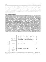
2. Electrochemical redox mediator
The electrochemical reduction reaction generated in cathode can’t catalyze reduction of
NAD
+
or NADP
+
both in vitro and in vivo without electron mediator. Various ion radicals
that are methyl viologen, benzyl viologen, hydroquinone, tetracyanoquinodimethane, and
Bioelectrochemical Fixation of Carbon Dioxide with Electric Energy Generated by Solar Cell
189
neutral red (NR) have been used as electron mediator to induce electrochemical redox
reaction between electrode and electron carriers that are NAD
+
, FAD, and cytochrome C
(Pollack et al., 1996; Park et al., 1997; Wang and Du, 2002; Kang et al., 2007). In order to in
vivo drive and maintain bacterial metabolism with electrochemical reducing power as a sole
energy source, only NAD
+
or NADP
+
is required to be reduced by coupling redox reaction
between electron mediator and biochemical electron carrier (Park and Zeikus, 1999; 2000).
NR can catalyze the electrochemical reduction reaction of NAD
+
both in vivo and in vitro but
no electron mediator except the NR can. NR is a water-soluble structure composed of
phenazine ring with amine, dimethyl amine, methyl, and hydrogen group as shown in Fig 1.
The dimethyl amine group is redox center for electron-accepting and donating in coupling
with phenazine ring; meanwhile, the amine, methyl, and hydrogen are structural group.
Redox potential of NR is -0.325 volt (vs. NHE), which is 0.05 volt lower than NAD
+
. The
electrochemical redox reaction of NR can be coupled to biochemical redox reaction as
follows:
[ NR
ox
+ 2e
-
+ 1H
+
NR
red
; NR
red
+ NAD
+
NR
ox
+ NADH ]
NAD
+
can be reduced in coupling with biochemical redox reaction as follows:
[ NAD
+
+ 2e
-
+ 2H
+
NADH + H
+
]
Commonly, NR
ox
and NAD
+
are reduced to NR
red
and NADH, respectively by accepting
two electrons and one proton.
Fig. 1. Molecular structure of neutral red, which can be electrochemically oxidized (A) or
reduced (B). The reduced neutral red can catalyze reduction reaction of NAD
+
(C) to NADH
(D) without enzyme catalysis. Ox and Red indicate oxidation and reduction, respectively.
Solar Cells – New Aspects and Solutions
190
Theoretically, the water-soluble NR may be reduced at the moment when contacted with
electrode and catalyze biochemical reduction of NAD
+
at the moment when contacted with
bacterial cell or enzyme. A part of NR may be contacted with electrode or bacterial cell in
water-based reactant but most of that is dissolved or dispersed in the reactant. In order to
induce the effective electrochemical and biochemical reaction in the bacterial culture, NR
and bacterial cells have to contact continuously and simultaneously with electrode. This can
be accomplished by immobilization of NR in graphite felt electrode based on the data that
most of bacterial cells tend to build biofilm spontaneously on surface of solid material and
the graphite felt is matrix composed of 0.47m
2
/g of fiber (Park et al., 1999). The amino group
of NR can bind covalently to alcohol group of polyvinyl alcohol by dehydration reaction, in
which polyvinyl-3-imino-7-dimethylamino-2-methylphenazine (polyvinyl-NR) is produced
as shown in Fig 2. The polyvinyl-NR is a water-insoluble solid electron mediator to catalyze
electrochemically reduction reaction of NAD
+
like the water-soluble NR (Park and Zeikus,
2003). The polyvinyl-NR immobilized in graphite felt (NR-graphite) functions as a cathode
for electron-driving circuit, an electron mediator for conversion of electric energy to
electrochemical reducing power, and a catalyst for reduction of NAD
+
to NADH. The
electrochemical bioreactor equipped with the NR-graphite cathode is very useful to cultivate
autotrophic bacteria that grow with carbon dioxide as a sole carbon source and
electrochemical reducing power as a sole energy source (Lee and Park, 2009).
3. Separation of electrochemical redox reaction
The biochemical reducing power can be regenerated electrochemically by NR-graphite
cathode (working electrode) that functions as a catalyst, for which H
2
O has to be
electrolyzed on the surface of anode (counter electrode) that functions as an electron donor.
The working electrode is required to be separated electrochemically from the counter
electrode by specific septa that are the ion-selective Nafion membrane (Park and Zeikus,
2003; Kang et al., 2007; Tran et al., 2009), the ceramic membrane (Park and Zeikus, 2003;
Kang et al., 2007; Tran et al., 2009), the modified ceramic membrane with cellulose acetate
film (Jeon et al, 2009B), and the micro-pored glass filter, by which the electrochemical
reducing power in the cathode compartment can be maintained effectively. Jeon and Park
(2010) developed a combined anode that was composed of cellulose acetate film, porous
ceramic membrane and porous carbon plate as shown in Fig 3. The combined anode
functions as a septum for electrochemical redox separation between anode and cathode, an
anode for electron-driving circuit, and a catalyst for electrolysis of H
2
O. The major function
of anode is to supply electrons required for generation of electrochemical reducing power in
the working electrode (NR-graphite cathode), in which H
2
O functions as an electron donor.
The strict anaerobic bacteria that are methanogens, sulfidogens, and anaerobic fermenters
grow in the condition with lower oxidation-reduction potential than -300 mV (vs. NHE)
(Ferry, 1993; Gottschalk, 1985), which can be induced electrochemically inside of the carbon
fibre matrices of NR-cathode under only non-oxygen atmosphere. The NR-cathode can
catalyze biochemical regeneration of NADH and generation of hydrogen but can’t catalyze
scavenging of oxygen and oxygen radicals at around 25
o
C and 1 atm. The combined anode
can protect effectively contamination of catholyte with the atmospheric oxygen by
unidirectional evaporation of water from catholyte to atmosphere through the combined
anode as shown in Fig 4. The driving force for the unidirectional evaporation of water may
be generated naturally by the difference of water pressure between catholyte and outside
atmosphere (Jeon et al., 2009A).