Solar Cells New Aspects and Solutions Part 8 ppt
Bạn đang xem bản rút gọn của tài liệu. Xem và tải ngay bản đầy đủ của tài liệu tại đây (2.11 MB, 35 trang )
Solar Cells – New Aspects and Solutions
236
multicrystalline Si wafers, which are modified with fine metal particles, by simply
immersing the wafers in an hydrofluoric acid solution without a bias and a particular
oxidizing agent (Yae et al. 2006a, 2009). In previous papers, we reported that porous layer
formation by this etching for 24 h decreased the reflectance of Si and increased the solar cell
characteristics, which are not only photocurrent density but also photovoltage (Yae et al.
2003, 2005, 2006a, 2009).
2.2.1 Etching mechanism
The metal-particle-assisted hydrofluoric acid etching of Si proceeds by a local galvanic cell
mechanism requiring photoillumination onto Si or dissolved oxygen in the solution (Yae et
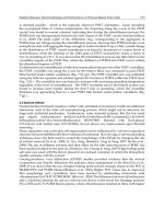
al. 2005, 2007d, 2009, 2010). Figure 5 shows a schematic diagram of n-Si and electrochemical
reaction (equations (5), (6) and (7)) potential in a hydrofluoric acid solution. The local cell
reaction consists of anodic dissolution of Si (equation (5)) and cathodic reduction of oxygen
(equation (6)) and/or protons (equation (7)) on catalytic Pt particles. Under the
photoillumination, photogenerated holes in the Si valence band anodically dissolve Si on the
whole photoirradiated surface of Si. Under the dark condition, the etching proceeds by holes
injected into the Si valence band with only cathodic reduction of oxygen on Pt particles, and
thus the etching is localized around the Pt particles. The localized anodic dissolution
produces macropores, which have Pt particles on the bottom, on the Si surface as shown in
Fig. 6. We previously revealed two points about metal-particle-assisted hydrofluoric acid
etching of Si: 1) the etching rate increased with photoillumination intensity on Si wafers and
dissolved oxygen concentration in hydrofluoric acid solution; and 2) the time dependence of
photoillumination intensity on the Si sample in the laboratory, which is ca. 0.2 mW cm
-2
illumination for 6 h, dark condition for 12 h and then ca. 0.2 mW cm
-2
illumination for 6 h, is
suitable to produce the macro- and microporous combined structure effective for improving
Fig. 5. Schematic diagram of silicon and electrochemical reaction potential in a hydrofluoric
acid solution.
Solar to Chemical Conversion
Using Metal Nanoparticle Modified Low-Cost Silicon Photoelectrode
237
the solar cell characteristics (Yae et al. 2005, 2006b, 2009). In this section, we applied this
method to the Pt-nanoparticle-modified multicrystalline n-Si to improve the solar cell
characteristics, and attempted to shorten the etching time by controlling etching conditions
such as the photoillumination intensity and the dissolved oxygen concentration.
Fig. 6. Typical cross-sectional scanning electron micrograph of silicon macropore having
a Pt particle on the bottom.
2.2.2 Porous structure control
The Pt-nanoparticle modified multicrytalline n-Si wafers were immersed in a 7.3 mol dm
-3
hydrofluoric acid aqueous solution at 298 K. In some cases, oxygen gas bubbling was applied
to the solution, and/or the n-Si wafers were irradiated with a tungsten-halogen lamp during
immersion in the solution in a dark room. The reflectance of Si wafers was measured using a
spectrophotometer in the diffuse reflection mode with an integrating sphere attachment.
Preparation
conditions
Pretreatment
Pt
deposition
time (s)
Prorous la
y
er formation (matal-
particle-assisted hydrofluoric
acid ethcing) conditions
Total etchin
g
time (h)
a A 120 without li
g
ht control for 24 h 24
b B 120 without li
g
ht control for 24 h 24
c B 120
under 40 mW cm
-2
with no
bubbling for 3 h
3
d B 120
40 mW cm
-2
with no bubblin
g
for
2 h and then in the dark with
oxygen bubbling for 4 h
6
e B 120
addin
g
under 40 mW cm
-2
with
oxygen bubbling for 0.5 h to
condition d
6.5
f B 60
40 mW cm
-2
with no bubblin
g
for
2 h and then in the dark with
oxygen bubbling for 4 h
6
g B 60
addin
g
under 40 mW cm
-2
with
oxygen bubbling for 0.5 h to
condition f
6.5
Table 1. Preparation conditions of Pt nanoparticle modified porous multicrystalline n-Si
Solar Cells – New Aspects and Solutions
238
The deposition conditions of Pt-nanoparticles and metal-particle-assisted hydrofluoric acid
etching conditions are listed in Table 1. Figure 7 shows typical scanning electron
microscopic images of multicrystalline n-Si wafers that were pretreated by method A (image
a) or B (image b) and metal-particle-assisted hydrofluoric acid etching without light control
for 24 h (conditions a and b in Table 1). Macropores, whose diameter is 0.3–1 m, were
formed on whole surfaces of multicrystalline n-Si wafers. The density of pores, i.e. porosity,
of n-Si wafer pretreated by method B is lower than that for method A. This is consistent with
the Pt particle density on multicrystalline Si surface before etching (Fig. 4a and b). Both
samples showed an orange photoluminescence under UV irradiation, thus microporous
layers were formed on both samples.
Fig. 7. Typical scanning electron microscopic images of Pt nanoparticle modified porous
multicrystalline n-Si. Preparation conditions: images a and b are for conditions a and b in
Table 1, respectively.
Figure 8 shows typical scanning electron microscopic images of multicrystalline n-Si that
were pretreated by method B and metal-particle-assisted hydrofluoric acid etching under
control of the photoillumination and the dissolved oxygen concentration (conditions c to g
in Table 1). A microporous layer giving photoluminescence and no macropores was
formed by etching under photoillumination without any gas bubbling estimated
dissolved oxygen concentration of solution is ca. 5 ppm (Fig. 8a, condition c). The etching
under the dark condition with oxygen gas bubbling (the solution was saturated with
oxygen) after the etching under photoillumination produced macro- and microporous
combined structure on the multicrystalline n-Si wafer (Fig. 8b, condition d). The
morphology of the Si surface is similar to that formed by the etching without light control
and gas bubbling for 24 h (Fig. 7b, condition b). Addition of the photoillumination with
oxygen bubbling to the preceding conditions enlarged the macropore size and
microporous layer thickness (Fig. 8c, condition e). Shortening the immersion time of
multicrystalline n-Si wafers in the Pt displacement deposition solution, i.e. reduction of
particle size and particle density of Pt on the wafers, reduced the number of macropores
on the etched n-Si wafers (Figs. 8d and e, conditions f and g, respectively). The structure
change in the porous layer of multicrystalline n-Si by changing the photoillumination
intensity and dissolved oxygen concentration is consistent with our previously reported
results on single crystalline n-Si (Yae et al., 2005, 2006b, 2009).
Solar to Chemical Conversion
Using Metal Nanoparticle Modified Low-Cost Silicon Photoelectrode
239
Fig. 8. Typical scanning electron microscopic images of Pt nanoparticle modified porous
multicrystalline n-Si. Preparation conditions: images a, b, c, d, and e are for conditions c, d,
e, f, and g in Table 1, respectively.
2.2.3 Antireflection effect
The macroporous layer formation changed the surface color of multicrystalline n-Si wafers to
dark gray. Figure 9 shows the reflectance spectra of multicrystalline n-Si wafers. The porous
layer prepared by the etching without light control and gas bubbling for 24 h reduced the
reflectance from over 30% to under 6.2% (curves a and b) (Yae et al., 2006a, 2009). The porous
layers prepared by the etching under the conditions d and g of Table 1 gave reflectance
between 8 and 17% (curves c and d). This value is higher than that of the wafer prepared
under the non-controlled conditions, but much lower than the non-etched wafer.
2.3 Photovoltaic photoelectrochemical solar cells
To evaluate electrical characteristics of photoelectrodes, we prepared photovoltaic
photoelectrochemical solar cells (Fig. 1a) equipped with the Pt-nanoparticle modified
porous multicrystalline n-Si photoelectrode. The multicrystalline n-Si electrode and Pt-plate
counterelectrode were immersed in a redox electrolyte solution. Just before measuring the
solar cell characteristics, the multicrystalline n-Si electrode was immersed in a 7.3 mol dm
-3
hydrofluoric acid solution for two min under the elimination of dissolved oxygen by
bubbling pure argon gas into the solution. This treatment is important to obtain high
photovoltage caused by halogen atom termination of Si surface as mentioned below. A
mixed solution of 7.6 mol dm
-3
hydroiodic acid (HI) and 0.05 mol dm
-3
iodine (I
2
) was used
Solar Cells – New Aspects and Solutions
240
as a redox electrolyte solution of the photovoltaic photoelectrochemical solar cell.
Photocurrent density versus potential (j-U) curves were obtained with a cyclic voltammetry
tool. The potential of the n-Si wafer was measured with respect to the Pt counterelectrode.
The multicrystalline n-Si was irradiated with a solar simulator (AM1.5G, 100 mW cm
-2
)
through the quartz window and a redox electrolyte solution ca. 3 mm thick.
Fig. 9. Reflectance spectra of multicrystalline n-Si wafers: curve a after immersion in sodium
hydroxide solution for saw damage layer removal; b, c, and d prepared under the conditions
a, d, and g in Table 1, respectively.
2.3.1 Effect of particle density and size of platinum nanoparticles
Figure 10 show typical photocurrent density versus potential (j-U) curves of Pt-nanoparticle
modified multicrystalline n-Si photoelectrodes having no porous layer pretreated under the
same conditions as the specimens of Fig. 4. The decrease in particle density and size of Pt-
nanoparticles increased the open-circuit photovoltage (V
OC
) and short-circuit photocurrent
density (j
SC
) of photovoltaic photoelectrochemical solar cells from curve a to curve c of Fig.
10. Thus, the conversion efficiency (
S
) of the solar cells increased from 3.8% to 5.0%.
The reason for the increase in photocurrent density of the photoelectrochemical solar cells is
the decrease of surface coverage of Pt-nanoparticles on Si. The surface coverage is 20% and
5% for Fig. 4a and b, respectively. This decrease is expected to increase the intensity of solar
light reaching the Si surface by 19%. This is almost consistent with the increase in the short-
circuit photocurrent density by 17%. The average open-circuit photovoltage of 12 samples is
0.42 V. This is lower than that for Pt-nanoparticle-electrolessly-deposited single crystalline
n-Si electrodes (0.50 V in the average of 76 samples). This is explained by the following two
reasons. 1) Lower quality of multicrystalline Si than single crystalline: The characteristics of
multicrystalline Si solar cells are commonly lower than those of single crystalline. Thus, not
only photovoltage but also the short-circuit photocurrent density and fill factor (F.F.) of
photoelectrochemical solar cells are 12.1 mA cm
-2
and 0.57 lower than those of single
Solar to Chemical Conversion
Using Metal Nanoparticle Modified Low-Cost Silicon Photoelectrode
241
crystalline (18.3 mA cm
-2
and 0.60 on average, respectively). 2) Insufficient density of
termination of Si surface bonds with iodine atoms: The termination of Si surface bonds with
iodine atoms shifts the flat band potential of Si toward negative, and thus increases the
photovoltage of photoelectrochemical solar cells using hydroiodic acid and iodine redox
electrolyte (Fujitani et al., 1997, Ishida et al., 1999, Yae et al., 2006a, Zhou et al., 2001). An
electrolyte solution of 8.6 mol dm
-3
hydrobromic acid (HBr) and 0.05 mol dm
-3
bromine (Br
2
)
has sufficient negative redox potential to generate high open-circuit photovoltage without
the termination. Using the hydrobromic acid and bromine electrolyte solution increases the
photovoltage by 0.06 V for multicrystalline and 0.03 V for single-crystalline n-Si electrodes
from those using hydroiodic acid and iodine electrolyte solution. This result indicates that
the density of the termination of multicrystalline n-Si surface bonds with iodine atoms is
insufficient for generating high photovoltage.
Fig. 10. Photocurrent density versus potential (j-U) curves of photovoltaic
photoelectrochemical solar cells equipped with Pt-nanoparticle modified multicrystalline
n-Si photoelectrode having no porous layer pretreated under the same conditions as the
specimens of Fig. 4. Pretreatment: method A (image a), B (b and c); Pt deposition time:
120 (a and b), 30 s (c).
2.3.2 Effect of porous layer
Table 2 and Figure 11 indicate the average characteristics and typical photocurrent density
versus potential (j-U) curves of photovoltaic photoelectrochemical solar cells equipped with a
Pt-nanoparticle modified porous multicrystalline n-Si electrode prepared under the conditions
listed in Table 1. The characteristics of photoelectrodes prepared under the conditions a and b
as those for the wafers indicated in Fig. 7 show that the combination of the controlling particle
density and size of Pt particles, and the formation of porous layer using metal-particle-assisted
etching obtained a large increase in the conversion efficiency (
S
) from 3.8% for curve a in Fig.
10 and 2.9% in average of 12 samples to 5.1% in the average (Table 2). The formation of
Solar Cells – New Aspects and Solutions
242
continuous microporous layer (Figs. 8a and 11a, and condition c in Table 1) increased
photovoltage (V
OC
), and decreased fill factor (F.F.) of the solar cells. The formation of macro-
and microporous combined structure (Figs. 8b and c, and conditions d and e in Table 1,
respectively) increased photocurrent density (j
SC
) and fill factor (F.F.), and thus increased the
conversion efficiency (
S
) of solar cells (Fig. 11b, and conditions d and e in Table 2). The
decrease of particle density and size of Pt particles (Figs. 8d and e, and conditions f and g in
Table 1, respectively) increased photocurrent density (j
SC
) and conversion efficiency (
S
) (Fig.
11c, and conditions f and g in Table 2). The conversion efficiency of solar cells reached 7.3% of
curve c in Fig. 11 and 6.1% in the average of 4 samples (Table 2), and the etching time was
shortened to 6.5 h from 24 h by controlling the photoillumination intensity and the dissolved
oxygen concentration during etching (condition g in Table 1 and 2).
Preparation
conditions see
Table 1
No. of
tested
samples
Ope
n
-circuit
photovoltage
V
OC
(V)
Short-circuit
photocurrent density
j
SC
(mA cm
-2
)
Fill factor
F.F.
Efficiency
S
(%)
a 21 0.47 13.8 0.60 3.9
b 7 0.50 16.6 0.62 5.1
d 17 0.46 17.6 0.60 4.9
e 3 0.50 17.4 0.63 5.5
f
3 0.49 18.0 0.66 5.8
g
4 0.50 19.5 0.63 6.1
Table 2. Characteristics of photovoltaic photoelectrochemical solar cells equipped with
Pt-nanoparticle modified porous multicrystalline n-Si electrode prepared under the
conditions in Table 1. Average values are indicated.
Fig. 11. Photocurrent density versus potential (j-U) curves of photovoltaic
photoelectrochemical solar cells equipped with a Pt-nanoparticle modified porous
multicrystalline n-Si electrode. Preparation conditions: curves a, b, and c, are for conditions
c, d, and g listed in Table 1, respectively.
Solar to Chemical Conversion
Using Metal Nanoparticle Modified Low-Cost Silicon Photoelectrode
243
The increase in photocurrent density of photoelectrochemical solar cells equipped with Pt-
nanoparticle modified multicrystalline n-Si electrode by the Pt-particle-assisted hydrofluoric
acid etching is ca. 15% lower than the 30-40% estimated with reduction of the reflectance
from 33% to 5-14% at the light wavelength of 700 nm. This difference can be explained by
the difference in the refractive index between air (1.000), water (1.332 at 633 nm) and Si
(3.796 at 1.8 eV (689 nm)) (Lide, 2004). The reflectance of Si is calculated at 34% in the air and
23% in the water. Using 23% as the initial value of reflectance estimates the increase in
photocurrent density by the etching at 12-23%. This value is consistent with the
experimental result of ca. 15%.
The photovoltage of photoelectrochemical solar cells equipped with Pt-nanoparticle
modified multicrystalline n-Si electrode was improved by formation of the porous layer by
Pt-particle-assisted hydrofluoric acid etching (Table 2). The photovoltage increase by the
etching in dark conditions for 24 h was 0.01 V (V
OC
: 0.43 V) in the average of eight samples,
much lower than the 0.05 V (V
OC
: 0.47 V) by the etching in a laboratory without light control
(condition a in Table 1 and 2). These results show that the microporous layer effectively
increases the photovoltage of such photoelectrochemical solar cells. This increase is
explained by the following two possible mechanisms. 1) Screening Pt-nanoparticles’
modulation of Si surface band energies by the microporous layer: The photovoltage of an n-
Si electrode modified with metal particles depends on the distribution density of metal
particles and the size of the direct metal-Si contacts. While metal particles are necessary as
electrical conducting channels and catalysts of electrochemical reactions, the particles
modulate the Si surface band energies. Thus, larger direct metal-Si contacts than a suitable
size and/or a higher distribution density of metal particles than a suitable value reduce the
effective energy barrier height, and then reduce the photovoltage of solar cells. The presence
of a moderately thick microporous layer between the metal particles and bulk n-Si screens
the modulation and thus raises the energy barrier height of the n-Si electrode, as discussed
in the previous paper (Kawakami et al., 1997). 2) Increase in density of termination of Si
surface bonds with iodine atoms: As we discussed in the previous section, the low open-
circuit photovoltage (0.42 V) of the flat (nonporous) multicrystalline n-Si electrodes can be
caused by the insufficient density of the termination of Si surface bonds with iodine atoms.
Using the hydrobromic acid and bromine electrolyte solution increased the average open-
circuit photovoltage of porous n-Si electrodes prepared under the condition a in Table 1 by
0.03 V for multicrystalline and 0.02 V for single-crystalline n-Si from those of using
hydroiodic acid and iodide electrolyte solution. This result indicates that the density of the
termination of the multicrystalline n-Si surface bonds with iodine atoms is increased to
sufficient value for generating high V
OC
by forming the microporous layer.
2.4 Solar to chemical conversion (solar hydrogen production)
In the preceding section, we prepared the efficient photovoltaic photoelectrochemical solar
cells using the Pt-nanoparticle modified porous multicrystalline n-Si electrode. In this section,
these electrodes were used for solar to chemical conversion via the photoelectrochemical
decomposition of hydrogen iodide (HI) to iodine (I
2
or I
3
-
) and hydrogen gas (H
2
), that is, solar
hydrogen. A two-compartment cell was used (Fig. 1b). The multicrystalline n-Si electrode was
used as a photoanode in the mixed solution of hydroiodic acid and iodine of the anode
compartment. A platinum plate was used as a counterelectrode in the perchloric acid (HClO
4
)
solution of the cathode compartment. Both compartments were separated with a porous glass
plate. Figure 12 shows the typical photocurrent density versus potential (j-U) curve for the
Solar Cells – New Aspects and Solutions
244
multicrystalline n-Si electrode prepared under the condition g in Table 1 and 2. The potential
(U) of the electrode was measured versus the Pt-plate counterelectrode in the perchloric acid
solution of the cathode compartment (Fig. 1b). The short-circuit photocurrent density of 21.7
mA cm
-2
was obtained. The solution color at the Si surface darkened, and gas evolution
occurred at the Pt cathode surface. These results clearly show that the photoelectrochemical
solar cell equipped with the Pt-nanoparticle modified porous multicrystalline n-Si electrode
can decompose hydrogen iodide into hydrogen and iodine with no external bias, as shown in
the equations (1), (2) and (3) in the section 1.1.
The dashed curve in Fig. 12 shows the current density versus the potential (j-U) curve of Pt
electrode, which was in the anode compartment, instead of the Si electrode of the above cell
for hydrogen iodide decomposition (Fig. 1b). The onset potential of the anodic current was
0.25 V versus the Pt-counterelectrode in the cathode compartment. This value indicates that
the Gibbs energy change for the hydrogen iodide decomposition in the present solutions is
0.25 eV. The energy gain of solar to chemical conversion using the photoelectrochemical
solar cell is calculated at 5.4 mW cm
-2
by the product of the Gibbs energy change per the
elementary charge and the short-circuit photocurrent density of 21.7 mA cm
-2
under
simulated solar illumination (AM1.5G, 100 mW cm
-2
). Thus, we calculate the efficiency of
solar to chemical conversion (solar hydrogen production) via the photoelectrochemical
decomposition of hydrogen iodide at 5.4%. The average in solar-to-chemical-conversion
efficiency of five samples was 4.7%.
Fig. 12. Photocurrent density versus potential (j-U) curve (solid line) for solar-to-chemical
conversion type of photoelectrochemical solar cell equipped with Pt-nanoparticle modified
porous multicrystalline n-Si electrode prepared under condition g in Table 1. The two-
compartment cell for photodecomposition of hydrogen iodide (Fig. 1b) was used. Dashed
line: Pt electrode measured in the anode compartment of the two-compartment cell instead
of the Si photoelectrode.
Solar to Chemical Conversion
Using Metal Nanoparticle Modified Low-Cost Silicon Photoelectrode
245
In Section 2, it was described that platinum-nanoparticle modified porous multicrystalline
silicon electrodes prepared by electroless displacement deposition and metal-particle-
assisted hydrofluoric acid etching can generate hydrogen (solar hydrogen) and iodine
through the photoelectrochemical decomposition of hydrogen iodide in aqueous solution
with no external bias at the solar-to-chemical conversion efficiency of 5.4%. The control of
particle density and size of Pt particles by changing the initial surface condition of Si and
deposition condition of Pt, and the control of porous layer structure by changing the etching
conditions improve the conversion efficiency.
3. Platinum nanoparticle modified microcrystalline silicon thin films
Hydrogenated microcrystalline silicon (c-Si:H) thin films are promising new materials for
low-cost solar cells. The microcrystalline Si thin film approach has several advantages,
including minimal use of semiconductor resources, large-area fabrication using low-cost
chemical vapor deposition (CVD) methods, and no photodegradation of the solar cell's
characteristics (Matsumura, 2001, Meier et al., 1994, Yamamoto et al., 1994). We applied
microcrystalline Si thin films to solar hydrogen production by the photodecomposition of
hydrogen iodide (Yae et al., 2007a, 2007b) and solar water splitting(Yae et al., 2007b). Figure
13 schematically shows a cross-section of the microcrystalline silicon thin-film
photoelectrode. Photoelectrochemical solar cells require neither a p-type semiconductor
layer nor a transparent conducting layer, which is necessary to fabricate solid-state solar
cells.
Fig. 13. Schematic cross-section of Pt-nanoparticle modified microcrystalline Si thin-film
photoelectrode.
3.1 Preparation of photoelectrodes and photovoltaic photoelectrochemical solar cells
Hydrogenated microcrystalline silicon thin films were deposited onto polished glassy
carbon (Tokai Carbon) substrates by the hot-wire catalytic chemical vapor deposition (cat-
CVD) method (Matsumura et al. 2003). A 40-nm-thick n-type hydrogenated microcrystalline
cubic silicon carbide (n-c-3C-SiC:H) layer was deposited on the substrates using hydrogen-
diluted monomethylsilane and phosphine gas at temperatures of 1700°C for the rhenium
filament. An intrinsic hydrogenated microcrystalline silicon (i-c-Si:H) layer, with thickness
of 2-3 m, was deposited on the n-type layer using monosilane gas at 1700°C for the
tantalum filament. The microcrystalline silicon thin film electrodes were prepared by
connecting a copper wire to the backside of the substrate with silver paste and covering it
with insulating epoxy resin.
Pt nanoparticle
i-
c-Si:H
n-c-3C-SiC:H
Carbon
Solar Cells – New Aspects and Solutions
246
We deposited the Pt nanoparticles on the microcrystalline silicon surface using electroless
displacement deposition as for the multicrystalline Si photoelectrodes (section 2.1). Figure 14
shows an scanning electron microscopic (SEM) image of the microcrystalline silicon film's
surface after immersion in the Pt deposition solution for 120 s. Platinum nanoparticles of 3-
200 nm in size and 1.5 x 10
10
cm
-2
in particle density were scattered on the film. The size and
distribution density of Pt particles varied with the deposition conditions, such as oxide layer
formation on the films before deposition and the immersion time of films in the deposition
solution. The distribution density is much higher than that for a single-crystalline n-Si
wafer, but the changing behaviors of the size and distribution density are similar to those of
the single crystalline (Yae et al., 2007c, 2008).
Fig. 14. Scanning electron microscopic image of Pt-nanoparticle modified microcrystalline
Si thin film surface.
0
2
4
6
8
10
-0.6 -0.5 -0.4 -0.3 -0.2 -0.1 0
j / mAcm
-2
U / V vs. Pt-counterelectrode
Fig. 15. Photocurrent density versus potential (j-U) curves for photovoltaic
photoelectrochemical solar cell equipped with the Pt-nanoparticle modified microcrystalline
Si photoelectrode measured in the 7.6 mol dm
-3
(M) hydroiodic acid (HI)/0.05 M iodine (I
2
)
(dashed line) and 3.0 M HI/0.002 M I
2
(solid line) redox solutions.
300 nm
Solar to Chemical Conversion
Using Metal Nanoparticle Modified Low-Cost Silicon Photoelectrode
247
For the photovoltaic photoelectrochemical solar cell (Fig. 1a), the Pt-nanoparticle-modified
microcrystalline silicon thin film electrode and Pt-plate counterelectrode were immersed in
a hydroiodic acid and iodine redox electrolyte solution as for the multicrystalline Si
photoelectrodes (section 2.3). Figure 15 shows the photocurrent density versus potential
(j-U) curves for the photovoltaic solar cell. The microcrystalline silicon film was stably
adherent to the glassy carbon substrate after completing the photoelectrochemical
measurements in these highly acidic solutions. The open-circuit photovoltage was 0.47-0.49
V. This is higher than the 0.3 V value obtained for the microcrystalline silicon thin film
electrode covered with a continuous 1.5-nm-thick Pt layer, which was deposited using the
electron-beam evaporation method. These results clearly indicate that the Pt-nanoparticle-
modified microcrystalline silicon thin film electrodes work by using the same mechanism as
the Pt-nanoparticle-modified single-crystalline n-Si electrodes, which work as ideal
semiconductor photoelectrodes for generating high photovoltage and stable photocurrent
described in previous sections 1.2 and 2.3.1. The reduction of redox electrolyte concentration
increased the short-circuit photocurrent density to 9.1 from 4.2 mA cm
-2
(Fig. 15, solid line).
This increase is caused by a decrease in the visible light absorption of the triiodide (I
3
-
) ion in
the redox solution. The increased photocurrent raised open-circuit photovoltage to 0.49 V,
and thus the photovoltaic conversion efficiency reached 2.7%.
3.2 Solar to chemical conversion (solar hydrogen production) via hydrogen iodide
decomposition
The Pt-nanoparticle modified microcrystalline Si thin film electrode were used for solar to
chemical conversion via the photoelectrochemical decomposition of hydrogen iodide to
iodine and hydrogen gas as the multicrystalline Si photoelectrodes (section 2.4). For the
photoelectrochemical decomposition of hydrogen iodide, a two-compartment cell was used
(Fig. 1b and 2).
0
2
4
6
8
10
-0.2 -0.1 0 0.1 0.2 0.3 0.4
j / mA cm
-2
U / V vs. Pt-counterelectrode in HBr
Fig. 16. Photocurrent density versus potential (j-U) curve (Solid line) for the Pt-nanoparticle
modified microcrystalline Si thin film electrode measured in the hydroiodic acid and iodine
mixture solution of the anode compartment of the two-compartment cell for solar to chemical
conversion (solar hydrogen production, Fig. 1b). Dashed line: Pt electrode measured in the
anode compartment of the two-compartment cell instead of the Si photoelectrode. Electrolyte
solutions: anode compartment: 3.0 M HI/0.002 M I
2
; cathode compartment: 3.0 M HBr.
Solar Cells – New Aspects and Solutions
248
The solid line in Fig. 16 shows the photocurrent density versus potential (j-U) curve for the
Pt-nanoparticle-modified microcrystalline Si thin film electrode measured in the hydroiodic
acid and iodine mixture solution of the anode compartment of the two-compartment cell.
The potential of the electrode was measured versus the Pt counterelectrode in the
hydrobromic acid solution of the cathode compartment. In the short-circuit condition under
the simulated solar illumination, we obtained a shirt-circuit photocurent density of 6.8 mA
cm
-2
, the solution color on the photoelectrode surface darkened, and gas evolution occurred
at the Pt cathode surface. These results clearly show that the photoelectrochemical solar cell
equipped with the Pt-nanoparticle-modified microcrystalline Si thin film electrode can
decompose hydrogen iodide into hydrogen gas and iodine with no external bias with 2.3%
of solar-to-chemical conversion efficiency.
3.3 Hydrogen production via solar water splitting using multi-photon system
A multi-photon system equipped with the microcrystalline Si thin film and titanium dioxide
(TiO
2
) photoelectrodes in series (Fig. 17) was prepared based on a work in literature using a
dye-sensitization-photovoltaic cell and a tungsten trioxide (WO
3
) photoanode (Grätzel,
1999). A titanium dioxide photoanode and a Pt cathode (counterelectrode) were immersed
in a perchloric acid (HClO
4
) aqueous solution in a quartz cell. A photovoltaic
photoelectrochemical solar cell equipped with the Pt-nanoparticle-modified microcrystalline
Si electrode (section 3.1) was connected to the titanium dioxide photoanode and Pt cathode
in series. Simulated solar light irradiated to the titanium dioxide photoelectrode. The
titanium dioxide, which has a 3-eV energy band gap, absorbs the short-wavelength part
(UV) of the solar light. The long-wavelength part of the solar light transmitted by the
titanium dioxide and quartz cell reaches the Pt-nanoparticle-modified microcrystalline Si
thin-film of the photovoltaic photoelectrochemical solar cell. The photovoltaic cell applies
bias between the titanium dioxide photoanode and the Pt cathode in a perchloric acid
aqueous solution for splitting water to hydrogen and oxygen.
Fig. 17. Schematic illustration of multi-photon system equipped with titanium dioxide and
microcrystalline Si photoelectrodes for solar water splitting.
e
-
e
-
Pt
Pt
TiO
2
n -Si
Light
HClO
4
aq.
HI -I
2
H
2
O
O
2
H
2
2H
+
Light
Pt
TiO
2
c-
Si:H
HI/I
2
aq.
Solar to Chemical Conversion
Using Metal Nanoparticle Modified Low-Cost Silicon Photoelectrode
249
The titanium dioxide photoanode was prepared as follows. Transparent conductive tin
oxide (SnO
2
)-coated glass plates were used as substrates. Titanium dioxide powder (P-25,
average crystallite size: 21 nm) was ground with nitric acid, acetyl acetone, surfactant
(Triton X-100), and water in a mortar. The obtained paste was coated on the substrate and
dried. The titanium dioxide-nanoparticle film was heated in air at 500°C for three hours. The
titanium dioxide electrode was prepared by connecting a copper wire to the bare part of the
conductive tin oxide film with silver paste and covering it with insulating epoxy resin.
-0.05
0
0.05
0.1
-0.2 0 0.2 0.4 0.6 0.8 1
j / mAcm
-2
U / V vs. Ag/AgCl
Fig. 18. Photocurrent density versus potential (j-U) curve for the titanium dioxide photoelectrode
in a perchloric acid aqueous solution under chopped simulated solar illumination.
-0.5 -0.4 -0.3 -0.2 -0.1 0
0
1
2
3
4
5
j / mAcm
-2
U / V vs. Pt-counterelectrode
Fig. 19. Photocurrent density versus potential (j-U) curve for the photovoltaic
photoelectrochemical solar cell equipped with a Pt-nanoparticle-modified microcrystalline
Si electrode in the redox solution under simulated solar light illumination through the
titanium dioxide photoelectrochemical cell.
Solar Cells – New Aspects and Solutions
250
Figure 18 shows the photocurrent density versus potential (j-U) curve for the titanium dioxide
photoelectrode in a perchloric acid aqueous solution under simulated solar illumination. The
dissolved oxygen in the solution was eliminated by using argon gas flow into the solution
before the measurement. The anodic photocurrent starts to generate at -0.14 V vs. Ag/AgCl.
This onset potential is more positive than -0.24 V vs. Ag/AgCl for hydrogen evolution, and
thus this electrode cannot split water into hydrogen and oxygen without external bias. Figure
19 shows the photocurrent density versus potential (j-U) curve for the photovoltaic
photoelectrochemical solar cell equipped with a Pt-nanoparticle-modified microcrystalline Si
electrode in the redox solution under simulated solar light illumination through the titanium
dioxide photoelectrochemical cell. The shirt-circuit photocurrent density was decreased from
5.3 mA cm
-2
for the cell under direct solar light illumination to 2.6 mA cm
-2
by light attenuation
with the titanium dioxide cell. The multi-photon system (Fig. 17) using the same titanium
dioxide and Pt-nanoparticle-modified microcrystalline Si electrodes as those in Figs. 18 and 19
indicated the photocurrent density versus potential (j-U) curve of Fig. 20. This system
generated anodic photocurrent at a potential that was more negative than -0.24 V vs. Ag/AgCl
for hydrogen evolution. Figure 21 shows that steady photocurrent was obtained for the multi-
photon system in the short-circuit condition (Fig. 17). Tiny gas bubble formed on the Pt
cathode during measurement under the short-circuit condition. These results show that this
multi-photon system can split water into hydrogen and oxygen with no external bias with
solar light. Since two photoelectrodes of titanium dioxide and Pt-nanoparticle-modified
microcrystalline Si were connected in series, photovoltage was the sum of the two electrodes'
values and photocurrent was the lower of the two electrodes' values. Therefore, the
photocurrent density for water splitting was determined by that of the titanium dioxide
electrode and very low. The photocurrent density, and thus hydrogen production by solar
water splitting, is expected to increase by using a semiconductor with a narrower band gap,
such as tungsten trioxide, instead of titanium dioxide. The theoretical simulation obtained
8 mA cm
-2
of shirt-circuit photocurrent density, that is, 10% of solar-to-chemical conversion
efficiency for solar water splitting for the tungsten trioxide and Si multi-photon system.
0
0.02
0.04
0.06
0.08
0.1
-0.5 0 0.5 1
j / mAcm
-2
U / V vs. Ag/AgCl
Fig. 20. Photocurrent density versus potential (j-U) curve for the multi-photon system (Fig. 17)
using the same titanium dioxide thin film and Pt-nanoparticle modified microcrystalline Si
photoelectrodes and electrolyte solutions as those in Figs. 18 and 19 under simulated solar
light illumination.
Solar to Chemical Conversion
Using Metal Nanoparticle Modified Low-Cost Silicon Photoelectrode
251
Fig. 21. Short-circuit photocurrent density (j) as a function of time (t) for the multi-photon
system of Fig. 20 under simulated solar illumination.
4. Conclusion
Multicrystalline silicon wafers and microcrystalline silicon thin films, which are common and
prospective low-cost semiconductor materials for solar cells, respectively, were successfully
applied to produce solar hydrogen via photodecomposition of hydrogen iodide and solar water
splitting. These photoelectrochemical solar cells have the following advantages: 1) simple
fabrication of a cell by immersing the electrode in an electrolyte solution; 2) there is no need for
a p-type semiconductor or a transparent conducting layer; and 3) direct solar-to-chemical
conversion (fuel production). Modification of silicon surface with platinum nanopartilces by
electroless displacement deposition and porous layer formation by metal-particle-assisted
hydrofluoric acid etching improve solar cell characteristics. The solar-to-chemical conversion
efficiency reached 5% for the photodecomposition of hydrogen iodide, and hydrogen gas
evolution was obtained by the solar water splitting with no input of external electricity.
5. Acknowledgment
The author is grateful to Prof. H. Matsuda, Dr. N. Fukumuro (University of Hyogo), Dr. S.
Ogawa, Prof. N. Yoshida, Prof. S. Nonomura (Gifu University), Mr. S. Sakamoto (Nippon
Oikos Co., Ltd.), and Prof. Y. Nakato (Osaka University) for co-work and valuable
discussions. The author would like to thank the students who collaborated: H. Miyasako, T.
Kobayashi, K. Suzuki, and A. Onaka. The author is grateful to Prof. Y. Uraoka of Nara
Institure of Science and Technology for the simulation of the solar water splitting using the
multi-photon system. The present work was partly supported by the following programs:
Grants-in-Aid for Scientific Research (C) from the JSPS (17560638, 20560676, and 23560875),
Grants-in-Aid for education and research from Hyogo Prefecture through the University of
Hyogo, Core Research for Evolutional Science and Technology (CREST) from the Japan
Science and Technology Agency (JST), and Research for Promoting Technological Seeds
from JST. The author wishes to thank Nippon Sheet Glass Co., Ltd. for donating transparent
conductive tin oxide coated glass plates. Figures 15 and 16 were reprinted from ref. Yae et
al., 2007a, copyright Elsevier (2007).
Solar Cells – New Aspects and Solutions
252
6. References
Allongue, P., Blonkowski, S., & Souteyrand, E. (1992). Elecrochim. Acta, Vol. 37, 781.
Arakawa, H., Shiraishi, C., Tatemoto, M., Kishida, H., Usui, D., Suma, A., Takamisawa, A.,
& Yamaguchi, T. (2007). Proc. SPIE, Vol. 6650, Solar Hydrogen and Nanotechnology II,
Guo, J. (Ed.), San Diego, 665003.
Chemla, M., Homma, T., Bertagna, V., Erre, R., Kubo, N., & Osaka, T. (2003). J. Electroanal.
Chem., Vol. 559, 111.
Fujishima, A. & Honda, K. (1972). Nature, Vol. 238, 37.
Fujitani, M., Hinogami, R., Jia, J. G., Ishida, M., Morisawa, K., Yae, S., & Nakato, Y. (1997).
Chem. Lett., 1041.
Grätzel, M. (1999). Cattech, Vol. 3, 4.
Gorostiza, P., Servat, J., Morante, J. R., & Sanz, F. (1996). Thin Solid Films, Vol. 275, 12.
Gorostiza, P., Allongue, P., Díaz, R.; Morante, J. R., & Sanz, F. (2003). J. Phys. Chem. B, Vol.
107, 6454.
Hinogami, R., Nakamura, Y., Yae, S., & Nakato, Y. (1997). Appl. Surf. Sci., Vol. 121/122, 301.
Hinogami, R., Nakamura, Y., Yae, S., & Nakato, Y. (1998). J. Phys. Chem. B, Vol. 102, 974.
Ishida, M., Morisawa, K., Hinogami, R., Jia, J. G., Yae, S., & Nakato, Y. (1999). Z. Phys. Chem.,
Vol. 212, 99.
Jia, J G., Fujitani, M., Yae, S., & Nakato, Y. (1996). Electrochim. Acta, Vol. 42, 431.
Kawakami, K., Fujii, T., Yae S., & Nakato, Y. (1997). J. Phys. Chem. B, Vol. 101, 4508.
Khaselev, O. & Turner, J. A. (1998). Science, Vol. 280, 542.
Licht, S. (Vol. Ed.). (2002). Semiconductor Electrodes and Photoelectrochemistry, Bard. A. J. &
Stratmann, M. (Series Eds.), Encyclopedia of Electrochemistry, Vol. 6, Wiley-VCH,
Weinheim.
Lide, D. R. (Ed.). (2004). CRC Handbook of Chemistry and Physics, CRC Press, Boca Raton, 85th
Ed., pp. 10-232, 10-234 and 12-150.
Lin, G. H., Kapur, M., Kainthla, R. C., & Bockris, J. O'M. (1989). Appl. Phys. Lett., Vol. 55, 386.
Matsumura, H. (2001). Thin Solid Films, Vol. 395, 1.
Matsumura, H., Umemoto, H., Izumi, A., & Masuda, A. (2003). Thin Solid Films, Vol. 430, 7.
Meier. J., Flückiger, R., Keppner, H., & Shah, A. (1994). Appl. Phys. Lett., Vol. 65, 860.
Miller, E. L., Marsen, B., Paluselli, D., & Rocheleau, R. (2005). Electrochem. Solid-State Lett.,
Vol. 8, A247.
Nagahara, L. A., Ohmori, T., Hashimoto, K., & Fujishima, A. (1993). J. Vac. Sci. Technol. A,
Vol. 11, 763.
Nakato, Y., Ueda, K., Yano, H., & Tsubomura, H. (1988). J. Phys. Chem., Vol. 92, 2316.
Nakato, Y. & Tsubomura, H. (1992). Elecrochim. Acta, Vol. 37, 897.
Nakato, Y., Jia, J. G., Ishida, M., Morisawa, K., Fujitani, M., Hinogami, R., & Yae, S. (1998).
Electrochem. Solid-State Lett., Vol. 1, 71.
Nakato, Y. (2000). Photoelectrochemical Cells, In: Wiley Encyclopedia of Electrical and
Electronics Engineering Online, Webster, J. (Ed.), John Wiley & Sons, Available from:
Nelson, J. (2003). The Physics of Solar Cells, Imperial College Press, London, pp. 276-279.
Paunovic, M., Schlesinger, M. (2006). Fundamentals of Electrochemical Deposition 2nd. Ed., John
Wiley & Sons, New York.
Solar to Chemical Conversion
Using Metal Nanoparticle Modified Low-Cost Silicon Photoelectrode
253
Park, J. H. & Bard, A. J. (2005). Electrochem. Solid-State Lett., Vol. 8, G371.
Sakai, Y., Sugahara, S., Matsumura, M., Nakato, Y., & Tsubomura, H. (1988). Can. J. Chem.,
Vol. 66, 1853.
Sze, S. M. (1981). Physics of Semiconductor Devices, John Wiley & Sons, New York, 2nd Ed.,
pp. 811-816.
Takabayashi, S., Nakamura, R., & Nakato, Y. (2004). J. Photochem. Photobiol. A, Vol. 166, 107.
Takabayashi, S., Imanishi, A., & Nakato, Y. (2006). Comptes Rendus Chimie, Vol. 9, 275.
Turner, J. A., Williams, M. C., & Rajeshwar, K. (2004). Interface, Vol. 13, No. 3, 24.
Yae, S., Tsuda, R., Kai, T., Kikuchi, K., Uetsuji, M., Fujii, T., Fujitani, M., & Nakato, Y. (1994).
J. Electrochem. Soc., Vol. 141, 3090.
Yae, S., Nakanishi, I., Nakato, Y., Toshima, N., & Mori, H. (1994). J. Electrochem. Soc., Vol.
141, 3077.
Yae, S., Fujitani, M., Nakanishi, I., Uetsuji, M., Tsuda, R., & Nakato, Y. (1996). Sol. Energy
Mater. Sol. Cells, Vol. 43, 311.
Yae, S., Kitagaki, M., Hagihara, T., Miyoshi, Y., Matsuda, H., Parkinson, B. A., & Nakato, Y.
(2001). Electrochim. Acta, Vol. 47, 345.
Yae, S., Kawamoto, Y., Tanaka, H., Fukumuro, N., & Matsuda, H. (2003). Electrochem. Comm.,
Vol. 5, 632.
Yae, S., Tanaka, H., Kobayashi, T., Fukumuro, N., & Matsuda, H. (2005). Phys. Stat. Sol. (c),
Vol. 2, 3476.
Yae, S., Kobayashi, T., Kawagishi, T., Fukumuro, N., & Matsuda, H. (2006). Solar Energy, Vol.
80, 701.
Yae, S., Kobayashi, T., Kawagishi, T., Fukumuro, N., & Matsuda, H. (2006). The
Electrochemical Society Proceedings Series, Vol. PV2004-19, Pits and Pores III: Formation,
Properties and Significance for Advanced Materials, Schmuki, P., Lockwood, D. J.,
Ogata, Y. H., Seo, M., & Isaacs, H. S. (Eds.). 141.
Yae, S., Kobayashi, T., Abe, M., Nasu, N., Fukumuro, N., Ogawa, S., Yoshida, N.,
Nonomura, S., Nakato, Y., & Matsuda, H. (2007). Sol. Energy Mater. Sol. Cells, Vol.
91, 224.
Yae, S., Onaka, A., Abe, M., Fukumuro, N., Ogawa, S., Yoshida, N., Nonomura, S., Nakato,
Y., & Matsuda, H. (2007). Proc. SPIE, Vol. 6650, Solar Hydrogen and Nanotechnology II,
Guo, J. (Ed.), San Diego, 66500E.
Yae, S., Nasu, N., Matsumoto, K., Hagihara, T., Fukumuro, N., & Matsuda, H. (2007).
Electrochim. Acta, Vol. 53, 35.
Yae, S., Abe, M., Kawagishi, T., Suzuki, K., Fukumuro, N., & Matsuda, H. (2007). Trans.
Mater. Res. Soc. Jpn., Vol. 32, 445.
Yae, S., Fukumuro, N., & Matsuda, H. (2008). Electrochemical Deposition of Metal
Nanoparticles on Silicon, In: Progress in Nanoparticles Research, Frisiras, C. T. (Ed.),
pp. 117-135, Nova Science Publishers, Inc., New York.
Yae, S., Fukumuro, N., & Matsuda, H. (2009). Porous Silicon Formation by Metal Particle
Enhanced HF etching, In: Electroanalytical Chemistry Research Trends, Hayashi, K.
(Ed.), pp. 107-126, Nova Science Publishers, New York.
Yae, S., Tashiro, M., Abe, M., Fukumuro, N., & Matsuda, H. (2010). J. Electrochem. Soc., Vol.
157, D90.
Solar Cells – New Aspects and Solutions
254
Yamamoto, K., Nakashima, A., Suzuki, T., Yoshimi, M., Nishio, H., & Izumina, M. (1994).
Jpn. J. Appl. Phys. Vol. 33, L1751.
Zhou, X., Ishida, M., Imanishi, A., & Nakato, Y. (2001). J. Phys. Chem. B, Vol. 105, 156.
12
Progress in Organic
Photovoltaic Fibers Research
Ayse Bedeloglu
Dokuz Eylül University,
Turkey
1. Introduction
Energy management including production, distribution and usage of energy is an important
issue, which determines internal and external policy and economical situation of countries.
For generating electrical energy, use of traditional energy sources in particular fossil based
fuels through long ages, caused environmental problems, in recent years. Renewable energy
technologies using power of wind, sun, water, etc. can be remedies to hinder negative
effects of pollution, emissions of carbon dioxide and irreversible climate change problem,
which it caused. Photovoltaic technology, which converts photons of the sun into electrical
energy by using semiconductors, is one of the most environmental friendly sources of
renewable energy (Dennler et al., 2006a). Solar cells are used in many different fields such as
in solar lambs and calculators, on roofs and windows of buildings, satellites and space craft,
textile structures (fibers, fabrics and garments) and accessories (bags and suitcases).
In addition, there is an increasing interest in organic electronics from a wide range of science
disciplines in which researchers search for novel, efficient and functional materials and
structures. Organic materials based optoelectronic devices such as organic photovoltaics
(organic solar cells), organic light emitting diodes and organic photo detectors (Curran et al.,
2009) are desirable in many applications due to interesting features of organic materials such
as cost advantage and flexibility. Production of electrical energy, which is necessary in both
industrial and human daily life by converting sunlight using organic solar cells (organic
photovoltaic technology) via easy and inexpensive techniques is also very interesting
(Günes et al., 2007).
A photovoltaic textile, which is formed by combining a textile structure with a solar cell, and
on which carries physical properties of textile and working principle of solar cell together,
can generate electricity for powering different electrical devices. Photovoltaic fiber
providing more compatibility to textiles in terms of flexibility and lightness owing to its thin
and polymer-based structure may be used in a wide variety of applications such as tents,
jackets, soldier uniforms and marine fabrics. This review is organized as follows: In the first
section, an overview of photovoltaic technology, smart textiles and photovoltaic textiles will
be presented. In the second section, a general introduction to organic solar cells and organic
semi conductors, features, the working principle, manufacturing techniques, and
characterization of organic solar cells as well as polymer based organic solar cells and
studies about nanofibers and flexible solar cells will be given. In the third part, recent
studies about photovoltaic fiber researches, production methods, and materials used and
Solar Cells – New Aspects and Solutions
256
application areas will be recounted. Finally, suggestions on future studies and the
conclusions will be given.
1.1 Photovoltaic technology
“Photovoltaic” is a marriage of two words: “photo”, which means light, and “voltaic”,
which means electricity. Electrical energy produced by solar cells is one of the most
promising sustainable alternative energy and can provide energy demand of the world, in
the future (Green, 2005). Today, silicon based solar cells having the highest power
conversion efficiency are dominated in the market; however they have still high production
costs. Electricity generation by solar cells is still more expensive than that of fossil fuels due
to materials and manufacturing processes used in solar cells and installation costs.
However, photovoltaic technology, compared to traditional energy production technologies,
have interesting features such as using endless and abundant source of sun’s energy, direct,
environmental friendly and noiseless energy generation without the need of additional
generators, customization according to requirements, having low maintenance costs and
portable modules producing power ranging between milliwatt to megawatts even in remote
areas, which make it unique (Dennler et al., 2006a). A photovoltaic system can convert sun
light into electricity on both sunny and cloudy days (European PhotoVoltaic Industry
Association (EPIA), 2009). The worldwide cumulative photovoltaic power installed reached
about 23GW, in the beginning of 2010 and produces about 25TWh of electricity on a yearly
basis (European PhotoVoltaic Industry Association (EPIA), 2010).
The electricity produced by solar cells can be utilized in many applications such as cooling,
heating, lighting, charging of batteries and providing power for different electrical devices
(Curran et al., 2009). Solar cells using silicon wafers are classified as first generation
technology having high areal production costs and moderate efficiency. Thin-film solar cells
using Amorphous silicon (a-Si), Cadmium telluride (CdTe) and Copper indium gallium
(di)selenide (CIGS) as second generation technology have advantages such as increased size
of the unit of manufacturing and reduction in material costs. However, this technology has
modest efficiency beside these advantages compared to first generation technology.
Therefore, third generation technology concept has been developed to eliminate
disadvantages of earlier photovoltaic technologies (Green, 2005). There are two approaches
in third generation photovoltaic technology. The first one aims to achieve very high
efficiencies and second one tries to achieve cost per watt balance via moderate efficiency at
low cost. Therefore, this uses inexpensive semiconductor materials and solutions at low
temperature manufacturing processes. The third generation photovoltaics use various
technologies and grouped under organic solar cells (Dennler et al., 2006a).
1.2 Smart textiles
Humankind has always been inspired to mimic intelligence of nature to create novel
materials and structures with fascinating functions. Over the last decades, in industrial and
daily life, paralleling to growth in world population and advancements in science and
technology, human requirements have changed and begun to diverge from each other.
Therefore, different functional products have emerged according to expectations and
requirements of human kind. One of these, intelligent materials, can coordinate their
characteristic behavior according to changes of external or internal stimulus (chemical,
mechanical, thermal, magnetic, electrical and so on) as in biological systems and have
different functions owing to their unique molecular structure (Mattila, 2006; Tani et al.,
Progress in Organic Photovoltaic Fibers Research
257
1998). Intelligent materials and structures can sense and react and more, adapt it and
perform a function of changes (Takagi, 1990; Tao, 2001).Intelligent material systems consist
of three parts: a sensor, a processor and an actuator. Intelligent materials can provide
advancements in many fields of science for energy generation, medical treatments, and
engineering applications and so on.
There are also many application areas for interactive textiles, which use intelligent materials
such as shape memory alloys or polymers, phase change materials, conductive materials
and etc. Intelligent textiles are defined as structures that are capable of sensing external and
internal stimuli and respond or adapt to them in a pre-specified way. Knowledge from
different scientific fields (biotechnology, microelectronics, nanotechnology and so on) is
required for intelligent textile research (Mattila, 2006). Intelligent textiles find uses in many
applications ranging from space to healthcare and entertainment.
Power supply by using discrete batteries is an important obstacle towards functionality of
intelligent textiles. Besides, flexibility, comfort and durability are other parameters
concerned to manufacture consistent products (Coyle & Diamond, 2010). Flexible solar cells
(Schubert & Werner, 2006), micro fuel cells (Gunter et al., 2007; enfucell, 2011), power
generation by body motion and body heat (Beeby, 2010; Starner, 1996) can be some
alternatives to the traditional batteries. Photovoltaic fibers and textiles can overcome this
power supply problem since they use the working principle of solar cells.
1.3 Photovoltaic textiles
Small electronic devices such as personal digital assistants, mobile phones, mp3 players, and
notebook computers, usually use traditional batteries of which energy is used up in a short
time. Integration of flexible solar cells into apparels and fabrics, which cells are positioned
in/on the textile, can provide required electrical energy for these portable electronic devices
(Schubert & Werner, 2006). Photovoltaic textiles can be formed by integrating solar cells into
textile structure or making textile structure itself from photovoltaic materials. Photovoltaic
textile research needs cooperation of different sciences consisting of textile, electronics,
physics and chemistry. Incorporation of solar cells with fibers and textiles that are flexible
can extend the applications of photovoltaics from military and space applications to lighting
and providing power for consumer electronics of humankind in daily usage.
Textile based solar cells are also named as photovoltaic textiles, solar textiles, energy
harvesting textiles, solar powered textiles in the literature. Photovoltaic textiles, which are
high value added intelligent products, and, which have a large application area, can benefit
textile industry by increasing its competitiveness with long term development.
Power conversion efficiency and price properties beside the flexibility, weight, comfort,
durability and washability properties of the products are also important from a customer
point of view. Position of the flexible solar cells on fabric is also important to take efficient
irradiation from the light source. Places of needed wires, controllers and batteries, which
have to be lightweight under the cloth, are needed to be concerned to develop viable
photovoltaic textiles (Schubert & Werner, 2006).
In recent years, there has been an increase in studies about developing photovoltaic fibers
which can take charge in different textile and clothing applications. An active photovoltaic
fiber, which is produced by using advanced design and suitable materials, and, which
consist of adequate smooth layers, efficiency and stability, is capable of forming a flexible
fabric by suitable knitting or weaving techniques, or integrating as a yarn into a cloth to
generate power for electronic devices by converting sunlight (DeCristofano, 2009)
Solar Cells – New Aspects and Solutions
258
Fiber based photovoltaics take the advantage of being flexible and lightweight. Integration
of photovoltaic fibers into fabrics and clothes is easy to manufacture wearable technology
products. Small surface of a fiber also provide large area photoactive surfaces in the case of
fabric, so higher power conversion efficiency can be obtained.
Traditional solar cells using silicon based semiconductors are generally rigid and are not
suitable to be used with textiles. The thin film solar cells based on inorganic semiconductors
can be made flexible and however they are more suitable for patching onto fabrics (Schubert
& Werner, 2006).
Inexpensive electricity production can be achieved, when both low-cost and high efficient
manufacturing of photovoltaic cells are achieved. A potential alternative approach to
conventional rigid solar cells is organic solar cells, which can be coated on both rigid and
flexible substrates using easy processing techniques. In addition, the polymer based organic
solar cells can be used to produce fully flexible photovoltaic textiles easily, in any scale, from
fibers to fabrics and using low-cost methods.
2. Organic photovoltaic technology
2.1 Organic semiconductors
Organic semiconductors, which are generally considered as intrinsic wide band gap
semiconductors (band gap>1.4 eV), have many advantages to be used in solar cells. For
example, organic semiconductors of which electronic band gap can be engineered by
chemical synthesis with low-cost (Günes et al., 2007) have generally high absorption
coefficients.
Organic semiconductors consist of different chemical structures (Nunzi, 2002) including
polymers, oligomers, dendrimers, dyes, pigments, liquid crystals (Yilmaz Canli et al., 2010)
etc. In carbon-based semiconductors, conductivity is obtained by conjugation, which single
and double bonds between the carbon atoms alternate (Pope & Swenberg, 1999).
Conjugated organics are challenging materials for solar cells owing to their semiconducting
and light absorbing features. As a compound of organic solar cells, organic semiconductors
can be processed by thermal evaporation techniques or solution based coating or printing
techniques at low temperatures (Deibel & Dyakonov, 2010).
2.2 Organic solar cells
As a promising renewable energy source, organic photovoltaics have attracted attention
during the last decades resulting in significant progress in cell efficiency exceeded 5%
(AM1.5, 1000 W/m
2
) (Green et al., 2010) in the conventional bulk heterojunction solar cell
architecture consisting of a polymer donor and fullerene acceptor blend. Organic solar cells
achieving photovoltaic energy conversion by organic semiconductor or conductor are
compatible with flexible substrates like textiles for use in novel application areas.
Photovoltaic effect, production of electricity by converting photons of the sunlight, occurs in
an organic solar cell by the following steps (Nunzi, 2002): Absorption of photons of the light
in the solar cell and exciton (electron-hole pair) creation; separation of charges and carriers
generation from exciton dissociation; transport and then collection of charges by respective
electrodes (Günes et al., 2007; Nunzi, 2002)
There are some approaches such as using conjugated polymers (Antonradis et al., 1994) and
their blends (Granström et al., 1998; Halls et al., 1995; Yu & Heeger, 1995), small molecules
(Tang, 1986; Wöhrle & Meissner, 1991) polymer-small molecule bilayers (Jenekhe & Yi, 2000;
Progress in Organic Photovoltaic Fibers Research
259
Breeze et al., 2002) and their blends (Tang, 1986; Shaheen et al., 2001; Dittmer et al., 2000) or
combinations of inorganic-organic materials (O`Reagan & Graetzel, 1991; Greenham et al.,
1996; Günes et al., 2008; to develop organic solar cells (Güneş & Sariçiftçi, 2007). Mostly, two
concepts are considered in organic solar cell researches: first one, (Krebs, 2009a) which is the
most successful is using conjugated polymers (Fig. 1) with fullerene derivatives by solution
based techniques and second one is cooperating small molecular materials (as donor and
acceptor) by thermal evaporation techniques (Deibel & Dyakonov, 2010).
A conventional organic solar cell (Fig. 2) device is based on the following layer sequence: a
semi-transparent conductive bottom electrode (indium tin oxide (ITO)) or a thin metal
layer), a poly(3,4-ethylenedioxythiophene:poly(styrene sulfonic acid) (PEDOT:PSS) layer
facilitating the hole injection and surface smoothness, an organic photoactive layer (most
common poly(3- hexylthiophene):[6,6]-phenyl-C61-butyric acid methyl ester (P3HT:PCBM)) to
absorb the light and a metal electrode (Aluminum, Al and Calcium, Ca) with a low work
function to collect charges on the top of the device (Brabec et al., 2001a; Brabec et al., 2001b;
Padinger et al., 2003). To form a good contact between the active layer and metal layer, an
electron transporting layer (i.e. Lithium Fluoride, LiF) is also used (Brabec et al., 2002).
Fig. 1. Example of organic semiconductors used in polymer solar cells. Reprinted from Solar
Energy Materials and Solar Cells, 94, Cai, W.; Gong, X. & Cao, Y. Polymer solar cells: Recent
development and possible routes for improvement in the performance, 114–127, Copyright
(2010), with permission from Elsevier.
Solar Cells – New Aspects and Solutions
260
Fig. 2. Bulk heterojunction configuration in organic solar cells (Günes et al., 2007)
ITO is the most commonly used transparent electrode due to its good transparency in the
visible range and good electrical conductivity (Zou et al., 2010). However, ITO, which
exhibits poor mechanical properties on polymer based substrates, has limited
conductivity for fabricating large area solar cells and needs complicated techniques,
which tend to increase the cost of the solar cells (Zou et al., 2010). Indium availability is
also limited. To alleviate limitations arised from ITO, alternative materials are needed to
replace transparent conducting electrode. There are some approaches such as using
carbon nanotubes (CNTs) (Rowell et al., 2006; Glatthaar et al., 2005; (Celik) Bedeloglu et
al., 2011; Dresselhaus et al., 2001), graphenes (Eda et al., 2008), different conductive
polymers (i.e. PEDOT:PSS and its mixtures (Ouyang et al., 2005; Kushto et al., 2005;
Huang et al., 2006; Ahlswede et al., 2008; Zhou et al., 2008), metallic grids (Tvingstedt &
Inganäs, 2007; Kang et al., 2008), nanowires (Lee et al., 2008) for potential candidates to
substitute ITO layer and to perform as hole collecting electrode. In particular, CNTs have
a wide variety of application area due to their unique features in terms of thermal,
mechanical and electrical properties (Ajayan, 1999; Baughman et al., 2002). A nanotube
has a diameter of a few nanometers and from a few nanometers to centimeters in length.
Carbon nanotubes can be classified into two groups according to the number of
combinations that form their walls: Single-walled nanotubes (SWNTs) and multi-walled
nanotubes (MWNTs) (Wang et al., 2009) Recently, CNTs are used in solar cells and can
substitute ITO as a transparent electrode in organic solar cells (Rowell et al., 2006;
Glatthaar et al., 2005; (Celik) Bedeloglu et al., 2011; Dresselhaus et al., 2001).
In the organic solar cell, the photoactive layer, light absorbing layer, is formed by
combination of electron donor (p) and an electron accepting (n) materials (Deibel &
Dyakonov, 2010) C
60
, its derivatives and Perylen pigments are mostly used as electron