Solar Cells New Aspects and Solutions Part 11 pptx
Bạn đang xem bản rút gọn của tài liệu. Xem và tải ngay bản đầy đủ của tài liệu tại đây (1.87 MB, 35 trang )
16
AlSb Compound Semiconductor as
Absorber Layer in Thin Film Solar Cells
Rabin Dhakal, Yung Huh, David Galipeau and Xingzhong Yan
Department of Electrical Engineering and Computer Science,
Department of Physics, South Dakota State University, Brookings
SD 57007,
USA
1. Introduction
Since industrial revolution by the end of nineteenth century, the consumption of fossil fuels
to drive the economy has grown exponentially causing three primary global problems:
depletion of fossil fuels, environmental pollution, and climate change (Andreev and
Grilikhes, 1997). The population has quadrupled and our energy demand went up by 16
times in the 20
th
century exhausting the fossil fuel supply at an alarming rate (Bartlett, 1986;
Wesiz, 2004). By the end of 2035, about 739 quadrillion Btu of energy (1 Btu = 0.2930711 W-
hr) of energy would be required to sustain current lifestyle of 6.5 billion people worldwide
(US energy information administration, 2010). The increasing oil and gas prices, gives us
enough region to shift from burning fossil fuels to using clean, safe and environmentally
friendly technologies to produce electricity from renewable energy sources such as solar,
wind, geothermal, tidal waves etc (Kamat, 2007). Photovoltaic (PV) technologies, which
convert solar energy directly into electricity, are playing an ever increasing role in electricity
production worldwide. Solar radiation strikes the earth with 1.366 KWm
-2
of solar
irradiance, which amounts to about 120,000 TW of power (Kamat 2007). Total global energy
needs could thus be met, if we cover 0.1% of the earth’s surface with solar cell module with
an area 1 m
2
producing 1KWh per day (Messenger and Ventre, 2004).
There are several primary competing PV technologies, which includes: (a) crystalline (c-Si),
(b) thin film (a-Si, CdTe, CIGS), (c) organic and (d) concentrators in the market.
Conventional crystalline silicon solar cells, also called first generation solar cells, with
efficiency in the range of 15 - 21 %, holds about 85 % of share of the PV market (Carabe and
Gandia, 2004). The cost of the electricity generation estimates to about $4/W which is much
higher in comparison to $0.33/W for traditional fossil fuels (Noufi and Zweibel, 2006). The
reason behind high cost of these solar cells is the use of high grade silicon and high vacuum
technology for the production of solar cells. Second generation, thin film solar cells have the
lowest per watt installation cost of about $1/W, but their struggle to increase the market
share is hindered mainly due to low module efficiency in the range of 8-11% ((Noufi and
Zweibel, 2006; Bagnall and Boreland, 2008). Increasing materials cost, with price of Indium
more than $700/kg (Metal-pages, n.d.), and requirements for high vacuum processing have
kept the cost/efficiency ratio too high to make these technologies the primary player in PV
market (Alsema, 2000). Third generation technologies can broadly be divided in two
categories: devices achieving high efficiency using novel approaches like concentrating and
Solar Cells – New Aspects and Solutions
342
tandem solar cells and moderately efficient organic based photovoltaic solar cells (Sean and
Ghassan, 2005; Currie et al., 2008). The technology and science for third generation solar
cells are still immature and subject of widespread research area in PV.
1.1 Thin film solar cells
Second Generation thin film solar cells (TFSC) are a promising approach for both the
terrestrial and space PV application and offer a wide variety of choices in both device
design and fabrication. With respect to single crystal silicon technology, the most important
factor in determining the cost of production is the cost of 250-300 micron thick Si wafer
(Chopra et al., 2004). Thin-film technologies allow for significant reduction in semiconductor
thickness because of the capacity of certain materials for absorbing most of the incident
sunlight within a few microns of thickness, in comparison to the several hundred microns
needed in the crystalline silicon technology (Carabe and Gandia, 2004). In addition, thin-film
technology has an enormous potential in cost reduction, based on the easiness to make
robust, large-area monolithic modules with a fully automatic fabrication procedure. Rapid
progress is thus made with inorganic thin-film PV technologies, both in the laboratory and
in industry (Aberle, 2009).
Amorphous silicon based PV modules have been around for more than 20 years Chithik et
al. first deposited amorphous silicon from a silane discharge in 1969 (Chittik et al., 1969) but
its use in PV was not much progress, until Clarson found out a method to dope it n or p
type in 1976 (Clarson, n.d.) Also, it was found that the band gap of amorphous silicon can be
modified by changing the hydrogen incorporation during fabrication or by alloying a-Si
with Ge or C (Zanzucchi et al., 1977; Tawada et al. 1981). This introduction of a-Si:C:H alloys
as p-layer and building a hetero-structure device led to an increase of the open-circuit
voltage into the 800 mV range and to an increased short-circuit current due to the “window”
effect of the wideband gap p layer increasing efficiency up to 7.1% (Tawada et al. 1981,
1982). Combined with the use of textured substrates to enhance optical absorption by the
“light trapping” effect, the first a-Si:H based solar cell with more than 10% conversion
efficiency was presented in 1982 (Catalakro et al., 1982). However, there exists two primary
reasons due to which a-Si:H has not been able to conquer a significant share of the global PV
market. First is the low stable average efficiency of 6% or less of large-area single-junction
PV modules due to “Staebler–Wronski effect”, i.e. the light-induced degradation of the
initial module efficiency to the stabilized module efficiency (Lechner and Schad, 2002;
Staebler and Wronski, 1977). Second reason is the manufacturing related issues associated
with the processing of large (>1 m
2
) substrates, including spatial non-uniformities in the Si
film and the transparent conductive oxide (TCO) layer (Poowalla and Bonnet, 2007).
Cadmium Telluride (CdTe) solar cell modules have commercial efficiency up to 10-11% and
are very stable compound (Staebler and Wronski, 1977). CdTe has the efficient light
absorption and is easy to deposit. In 2001, researches at National Renewable Energy
Laboratory (NREL) reported an efficiency of 16.5% for these cells using chemical bath
deposition and antireflective coating on the borosilicate glass substrate from CdSnO
4
(Wu et
al., 2001). Although there has been promising laboratory result and some progress with
commercialization of this PV technology in recent years (First Solar, n.d.), it is questionable
whether the production and deployment of toxic Cd-based modules is sufficiently benign
environmentally to justify their use. Furthermore, Te is a scarce element and hence, even if
most of the annual global Te production is used for PV, CdTe PV module production seems
limited to levels of a few GW per year (Aberle, 2009).
AlSb Compound Semiconductor as Absorber Layer in Thin Film Solar Cells
343
The CIGS thin film belongs to the multinary Cu-chalcopyrite system, where the bandgap
can be modified by varying the Group III (on the Periodic Table) cations among In, Ga, and
Al and the anions between Se and S (Rau and Schock, 1999). This imposes significant
challenges for the realization of uniform film properties across large-area substrates using
high-throughput equipment and thereby affects the yield and cost. Although CIGS
technology is a star performer in laboratory, with confirmed efficiencies of up to 19.9% for
small cells (Powalla and Bonnet, 2007) however the best commercial modules are presently
11–13% efficient (Green et al. 2008). Also there are issues regarding use of toxic element
cadmium and scarcity of indium associated with this technology. Estimates indicate that all
known reserves of indium would only be sufficient for the production of a few GW of CIGS
PV modules (Aberle, 2009).
This has prompted researchers to look for new sources of well abundant, non toxic and
inexpensive materials suitable for thin film technology. Binary and ternary compounds of
group III-V and II-VI are of immediate concern when we look for alternatives. AlSb a group
III-V binary compound is one of the most suitable alternatives for thin film solar cells
fabrication because of its suitable optical and electrical properties (Armantrout et al., 1977).
The crystalline AlSb film has theoretical conversion efficiency more than 27% as suggested
in literature (Zheng et al., 2009).
1.2 Aluminum antimony thin films
Aluminum Antimony is a binary compound semiconductor material with indirect band gap of
1.62 eV thus ideal for solar spectrum absorption (Chandra et al., 1988). This also has become
the material of interest due to relatively easy abundance and low cost of Al and Sb. AlSb single
crystal has been fabricated from the Czochralski process but the AlSb thin film was prepared
by Johnson et al. by co-evaporation of Al and Sb. They also studied the material properties to
find out its donor and acceptor density and energy levels (Johnson, 1965). Francombe et al.
observed the strong photovoltaic response in vacuum deposited AlSb for the first time in 1976
(Francombe et al., 1976). Number of research groups around the world prepared thin AlSb thin
film and studied its electrical and optical properties by vacuum and non vacuum technique.
These include, Leroux et al. deposited AlSb films on number of insulating substrate by
MOCVD deposition technique in 1979 (Leroux et al., 1980). Dasilva et al. deposited AlSb film
by molecular beam epitaxy and studied its oxidation by Auger and electron loss spectroscopy
in 1991 (Dasilva et al., 1991). Similarly, AlSb film was grown by hot wall epitaxy and their
electrical and optical properties was studied by Singh and Bedi in 1998 (Singh and Bedi, 1998).
Chen et al. prepared the AlSb thin film by dc magnetron sputtering and studied its electrical
and optical properties (Chen et al. 2008) in 2007. Gandhi et al. deposited AlSb thin film on by
the alternating electrical pulses from the ionic solution of AlCl
3
and SbCl
3
in EMIC (1-methyl-
3-ethylimidazolium chloride) and studied its electrical and optical characters (Gandhi et al.
2008). However, AlSb thin film had never been successfully employed as an absorber material
in photovoltaic cells. We, electro-deposited AlSb thin film on the TiO
2
substrate by using the
similar technique as Gandhi et al. and had observed some photovoltaic response in 2009
(Dhakal et al., 2009). Al and Sb ions are extremely corrosive and easily react with air and
moisture. Thus it becomes very difficult to control the stoichiometry of compound while
electroplating. Thus, vacuum deposition techniques become the first choice to prepare AlSb
thin films for the solar cell applications. In this work, we fabricated AlSb thin film co-
sputtering of Al and Sb target. The film with optimized band-gap was used to fabricate p-n
and p-i-n device structures. The photovoltaic response of the devices was investigated.
Solar Cells – New Aspects and Solutions
344
2. Fabrication of AlSb thin films
AlSb film was prepared from dc magnetron sputtering of Al and Sb target (Kurt J. Lesker,
Materials Group, PA) simultaneously in a sputtering chamber. Sputtering is a physical
vapor deposition process whereby atoms are ejected from a solid target material due to
bombardment of the target by plasma, a flow of positive ions and electrons in a quasi-
neutral electrical state (Ohring, 2002). Sputtering process begins when the ion impact
establishes a train of collision events in the target, leading to the ejection of a matrix atom
(Ohring, 2002). The exact processes occurring at the target surface is depends on the energy
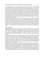
of the incoming ions. Fig. 1 shows the schematic diagram of sputtering using DC and RF
power. DC sputtering is achieved by applying large (~2000) DC voltages to the target
(cathode) which establishes a plasma discharge as Ar
+
ions will be attracted to and impact
the target. The impact cause sputtering off target atoms to substrates.
Fig. 1. Schematic Diagrams of (a) DC sputtering and (b) RF sputtering (Ohring, 2002)
AlSb Compound Semiconductor as Absorber Layer in Thin Film Solar Cells
345
In DC sputtering, the target must be electrically conductive otherwise the target surface will
charge up with the collection of Ar
+
ions and repel other argon ions, halting the process. RF
Sputtering - Radio Frequency (RF) sputtering will allow the sputtering of targets that are
electrical insulators (SiO
2
, etc). The target attracts Argon ions during one half of the cycle
and electrons during the other half cycle. The electrons are more mobile and build up a
negative charge called self bias that aids in attracting the Argon ions which does the
sputtering. In magnetron sputtering, the plasma density is confined to the target area to
increase sputtering yield by using an array of permanent magnets placed behind the
sputtering source. The magnets are placed in such a way that one pole is positioned at the
central axis of the target, and the second pole is placed in a ring around the outer edge of the
target (Ohring, 2002). This configuration creates crossed E and B fields, where electrons drift
perpendicular to both E and B. If the magnets are arranged in such a way that they create
closed drift region, electrons are trapped, and relies on collisions to escape. By trapping the
electrons, and thus the ions to keep quasi neutrality of plasma, the probability for ionization
is increased by orders of magnitudes. This creates dense plasma, which in turn leads to an
increased ion bombardment of the target, giving higher sputtering rates and, therefore,
higher deposition rates at the substrate.
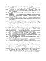
We employed dc magnetron sputtering to deposit AlSb thin films. Fig. 2 shows the
schematic diagram of Meivac Inc sputtering system. Al and Sb targets were placed in gun 1
and 2 while the third gun was covered by shutter. Both Al and Sb used were purchase from
Kurt J. Lesker and is 99.99% pure circular target with diameter of 2.0 inches and thickness of
0.250 inches.
Fig. 2. Schematic diagram of dc magtron sputtering of Al and Sb targets.
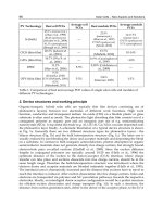
Firstly, a separate experiment was conducted to determine the deposition rate of aluminum
and antimony and the associated sputtering powers. Al requires more sputtering power
than Sb does for depositing the film at same rates. Next Al and Sb was co-sputtered to
Solar Cells – New Aspects and Solutions
346
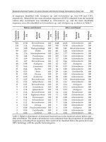
produce 1 micron AlSb film in different deposition ratio for Al:Sb. The film was annealed at
200 C in vacuum for 2 hrs and cooled down naturally. Table 1 summarizes the deposition
parameters of different AlSb films.
Al: Sb
Ratio
Deposition Rate
(Å/s)
Sputtering Power
(W)
Ar Gas Pressure
(mTorr)
Film Thickenss
(kÅ)
Al Sb Al Sb
1:3 2 6 104 37 20.1 10
2:5 2 5 104 33 20.1 10
3:7 3 7 150 42 20.1 10
1:1 1 1 150 24 20.1 10
7:3 7 3 261 24 20.1 10
Table 1. Deposition Parameters of Different AlSb films.
The film was deposited on glass slides for electrical and optical characterization. The
microscopic glass substrate (1 cm x 1 cm) was cleaned using standard substrate cleaning
procedure as follows: soaked in a solution of 90% boiling DI and 10% dishwashing liquid for
five minutes, followed by soaking in hot DI (nearly boiled) water for five minutes. The
substrate was then ultra sonicated, first in Acetone (Fisher Scientific) and then isopropyl
alcohol (Fisher Scientific) for 10 minutes each. The substrate was then blown dry with
nitrogen.
The morphology of the AlSb film was checked by SEM and was used to validate the grain
size and crystalline nature of AlSb particles and shown in Fig. 3.
(a) (b)
Fig. 3. SEM images of the AlSb thin film (a) before annealing, and (b) after annealing.
The AlSb grains were found to have been developed after annealing of the film due to proper
diffusion and bonding of Al and Sb. Only low magnified image could be produced before
annealing the film and holes were seen on the surface. The AlSb microcrystal is formed with
an average grain size of 200 nm. Also seen are holes in the film which are primarily the defect
area, which could act as the recombination centers. Better quality AlSb film could be produced
if proper heating of the substrate is employed during deposition process.
AlSb Compound Semiconductor as Absorber Layer in Thin Film Solar Cells
347
3. Optical characterization of AlSb thin film
The transmittance in the thin film can be expressed as (Baban et al. 2006):
0
1112131
d
T
I
TRRRSe
I
(1)
Where, α is the absorption coefficient antd d is the thickness of the semiconductor film. R1,
R2 and R3 are the Fresnel power reflection coefficient and the Fresnel reflection coefficient at
semiconductor - substrate and substrate – air interface. S measures the scattering coefficient
of the surface.
UV Visible Spectrophotometer (Lambda 850) was used to measure the absorption and
transmission data. This system covered the ultraviolet-visible range in 200 – 800 nm. The
procedures in the Lambda 850 manual were followed. Figure 4 shows the transmittance
spectra of the AlSb thin films. The films have an strong absorption in the visible spectral
range up to 550 nm for film with Al:Sb ratio 2:5. Similarly for films with Al:Sb in the ratio of
1:3, 1:1 and 3:7 have strong absorption up to 700 nm. The films were transparent beyond
these levels.
Fig. 4. Transmittance Spectra of AlSb films with different Al:Sb growth ratios.
The film with Al:Sb ratio of 7:3 didn’t have a clear transmittance spectra and thus not shown
in the figure. This was because the increasing the content of aluminum would make the film
metallic thus absorbing most of the light in visible spectrum.
Absorption coefficient of a film can be determined by solving equation 1 for absorption and
normalizing the Transmittance in the transparent region as (Baban et al. 2006):
1
ln
normalized
T
d
(2)
Optical band gap of the film was calculated with the help of transmission spectra and
reflectance spectra by famous using Tauc relation (Tauc, 1974)
n
g
hdhE
(3)
Solar Cells – New Aspects and Solutions
348
Where Eg is optical band gap and the constant n is 1/2 for direct band gap material and n is
2 for indirect band gap. The value of the optical band gap, Eg, can be determined form the
intercept of
12
h
Vs Photon energy, hν, at
12
h
= 0.
Fig. 5. Bandgap estimation of AlSb semiconductor with Al:Sb growth ratios (a) 1:3, (b) 2:5,
(c) 1:1 and (d) 3:7.
The optical absorption coefficient of all the films was calculated from the transmittance spectra
and was found in the range of 10
5
cm
-1
for photon energy range greater than 1.2 eV. Fig. 5
shows the square root of the product of the absorption coefficient and photon energy (
hν) as a
function of the photon energy. The band gap of the film was then estimated by extrapolating
the straight line part of the (αhv)
1/2
vs hν curve to the intercept of horizontal axis.
This band gap for Al:Sb growth ratio 1:3, 2:5, 1:1 and 3:7 was found out to be 1.35 eV, 1.4 eV,
1.25 eV and 1.44 eV respectively. Since the ideal band gap of AlSb semiconductor is 1.6 eV we
have taken the Al:Sb growth ratio to be 3:7 to characterize the film and fabricate the solar cells.
4. Electrical characterization
Material’s sheet resistivity, ρ, can be measured using the four point probe method as show
in Fig. 6. A high impedance current source is used to supply current (
I) through the outer
two probes and a voltmeter measures the voltage (
V) across the inner two probes.
AlSb Compound Semiconductor as Absorber Layer in Thin Film Solar Cells
349
Fig. 6. Schematic diagram of Four point probe configuration.
The sheet resistivity of a thin sheet is given by (Chu et al. 2001):
measured
measured
V
RCF
I
(4)
Where, RCF is the resistivity correction factor and given by
ln 2
RCF
The sheet resistance,
R
s
, could be thus be calculated as R
s
= ρ/d and measured in ohms per square. Conductivity
(
σ) is measured as reciprocal of resistivity and could be related to the activation energy as
(Chu et al., 2001):
0
E
kT
b
e
(5)
Where, ∆E is the activation energy. This describes the temperature dependence of carrier
mobility. The dark conductivity of AlSb film measured as a function of temperature
and is
shown in Fig. 7.
Fig. 7. Temperature dependence of annealed AlSb (3:7) film when heated from 26 - 240 ˚C
(dot line for guiding the eyes).
Solar Cells – New Aspects and Solutions
350
The annealed film shows a linear lnσ vs 1/T relationship. The activation energy of the dark
conductivity was estimated to be 0.68 eV from the temperature dependence of the
conductivity curve for AlSb film. This value is in good agreement with work done by Chen
et al. (Chen et al., 2008). This curve also confirms the semiconducting property of the AlSb
(3:7) film because the conductivity of the film was seen to be increasing with increasing the
excitation.
5. Simulation of solar cell
AMPS 1D beta version (Penn State Univ.) was used to simulate the current voltage
characteristics of p-
i-n junction AlSb solar cells. The physics of solar cell is governed by three
equations: Poisson’s equation (links free carrier populations, trapped charge populations,
and ionized dopant populations to the electrostatic field present in a material system), the
continuity equations (keeps track of the conduction band electrons and valence band holes)
for free holes and free electrons. AMPS has been used to solve these three coupled non-
linear differential equations subject to appropriate boundary conditions. Following
simulation parameters was used for the different layers of films.
Contact Interface
Barrier Height (eV) 0.1 (E
C
-E
F
) 0.3 (E
F
-E
V
)
S
e
(cm/s) 1.00 × 10
8
1.00 × 10
8
S
h
(cm/s) 1.00 × 10
8
1.00 × 10
8
* S surface recombination velocity of electrons or holes.
Semiconductor Layers
CuSCN AlSb ZnO TCO
Thicknesses, d (nm) 100 1000 45 200
Permittivity,
/
0
10 9.4 10 9
Band gap,
E
g
(eV) 3.6 1.6 2.4 3.6
Density of electrons on conduction band, N
C
(cm
-3
)
1.80 × 10
18
7.80 × 10
17
2.22× 10
18
2.22× 10
18
Density of holes on valence band,
N
V
(cm
-3
) 2.20× 10
19
1.80× 10
19
1.80× 10
19
1.80× 10
19
Electron mobility,
µ
e
(cm
2
/Vs) 100 80 100 100
Hole mobility,
µ
p
(cm
2
/Vs) 25 420 25 25
Acceptor or donor density,
N
A
or N
D
(cm
-3
)
N
A
=
1× 10
18
N
A
=
1× 10
14
N
D
=
1.1× 10
18
N
D
=
1× 10
18
Electron affinity,
Χ (eV) 4.5 4.5
* ε
0
= 8.85×10
-12
F/m electric constant; TCO is In
2
O
3
: SnO
2
.
Gaussian Midgap defect states
N
DG
, N
AG
(cm
-3
)
A = 1×
10
19
D = 9×
10
10
A = 1×
10
19
D = 1×
10
16
W
G
(eV) 0.1 0.1 0.1 0.1
σ
e
(cm
2
) 1.00 × 10
-13
1.00 × 10
-8
1.00 × 10
-16
1.00 × 10
-11
σ
p
(cm
2
) 1.00 × 10
-13
1.00 × 10
-11
1.00 × 10
-13
1.00 × 10
-14
* N
DG/AG
the donor-like or acceptor-like defect density, W
G
the energy width of the Gaussian distributio
n
for the defect states, τ carrier lifetime, and σ capture cross section of electrons (σ
e
) or holes (σ
p
).
Table 2. Parameters of the simulating the IV behavior or p-i-n junction solar cells.
AlSb Compound Semiconductor as Absorber Layer in Thin Film Solar Cells
351
Fig. 8. Current-voltage simulation of AlSb p-i-n junction structure in AMPS 1D software.
Fig. 8 shows the current voltage simulation curve of pin junction solar cell - CuSCN/AlSb/ZnO
with AlSb as an intrinsic layer. CuSCN was used as a p layer and ZnO as a n layer. The cell was
illuminated under one sun at standard AM 1.5 spectrum.
The simulation result shows that the solar cell has the FF of 55.5% and efficiency of 14.41%.
The short circuit current for the cell was observed to be 21.7 mA/cm
2
and the open
circuit voltage was observed to be 1.19 V. AlSb is thus the promising solar cell material for
thin film solar cells. The efficiency of the same cell structure could be seen increased up to
19% by doubling the thickness of AlSb layer to 2 micron.
6. Solar cell fabrication
Both p-n and p-i-n junction solar cells were designed and fabricated in 1cm x 2 cm substrate
with AlSb as a p type and an absorber material respectively. Variety of n type materials
including TiO
2
and ZnO were used to check the photovoltaic response of AlSb thin film. Fig.
9 shows the p-n and p-
i-n based solar cell design with ZnO and TiO
2
are an n-type layer and
CuSCN as a p-type layer.
Fig. 9. Solar Cell Design (a) p-n and (b) p-
i-n structure.
Solar Cells – New Aspects and Solutions
352
ZnO thin film was prepared by RF sputtering of 99.999% pure ZnO target (Kurt J. Lesker,
PA, diameter 2 inches and thickness 0.25 inches). ZnO intrinsic film was deposited by RF
power of 100 W at 0.7 Å/s and subsequently annealed in air at 150
0
C. ITO film was also
prepared from 99.99% pure ITO target (Kurt J. Lesker, PA, diameter 2 inches and thickness
0.25 inches) on the similar fashion using dc magnetron sputtering. Transparent ITO film was
deposited at plasma pressure of 4.5 mTorr. The sputtering power of 20 W yields deposition
rate 0.3 Å/s. The film was then annealed at 150
0
C in air for 1 hour. The highly ordered
mesoporous TiO
2
was deposited by sol gel technique as described by Tian et al. (Tian et al.
2005). CuSCN thin film was prepared by spin coating the saturated solution of CuSCN in
dipropyl sulphide and dried in vacuum oven at 80
0
C (Li et al., 2011). The thickness of all
three films ZnO, ITO and TiO
2
film was about 100 nm and the thickness of AlSb layer is ~1
micron. The active layer was annealed.
7. I-V Characterization of solar cell
Current voltage measurement of the solar cells was carried out using Agilent 4155c (Agilent,
Santa Clara, CA) semiconductor parameter analyzer equipped with solar cell simulator in
SDSU. Fig. 10 shows the experimental set up used for measuring I-V response of the solar cells,
where 2 SMUs (source measurement unit) were used. The SMU s could operate as a voltage
source (constant sweep voltage) or a current source and it could measure voltage and current
at the same time. The SMUs could measure from 10
-12
A to 1 A and -10 V to 10 V. SMU 1 was
set as voltage sweep mode from -1 V to 1 V with steps of 0.01 V, and SMU 2 was set to
measure current of the solar cell during IV measurement. IV responses were measured under
both dark and illuminated condition. During illumination, the intensity of the simulated light
was 100 mW·cm
-2
and calibrated using the NREL calibrated standard cell.
Fig. 10. Experimental set up for measuring IV response of a solar cell.
Table 3 shows the current voltage characteristics of p-n junction solar cells with structures
AlSb/TiO
2
, AlSb/ZnO. The active cell area was 0.16 cm
2
and fabricated on ITO coated glass
surface.
The
Voc of the best cell with ZnO as an n type layer was found out to be 120 mV and Isc to
be 76 uA. The
FF of the cell was calculated to be 0.24 and the efficiency was 0.009%. The cell
with TiO
2
as an n layer has even lower V
OC
and Isc. TiO
2
is less suitable n-type layer for
making junction with AlSb than ZnO because it is far more conductive than TiO
2
. A number
of reasons may be attributed for this low efficiency. First, is due to small electric field at the
junction between AlSb and the n type material (ZnO or TiO
2
). This severely limits the charge
AlSb Compound Semiconductor as Absorber Layer in Thin Film Solar Cells
353
separation at the junction and decreases V
OC
of the device. A better material needs to be
explored to dope AlSb n type to increase the built in field. The field could also be extended
using the p-
i-n structure to design the solar cells.
Cell V
OC
(mV) I
SC
(mA) FF Efficiency %
AlSb/TiO2 80 12x10
-3
0.23 0.001
AlSb/ZnO 120 76x10
-3
0.24 0.009
Table 3. Current-voltage characteristics of p-n junction solar cells
Interesting results were obtained with a p-
i-n junction, CuSCN/AlSb/ZnO. The used cell
has an active cell area of this cell was 0.36 cm
2
and fabricated on Mo coated glass surface.
Charge was collected from the silver epoxy fingers casted on top of ITO surface and Mo
back contact. The cell showed a
V
OC
of ~ 500 mV and a J
SC
of 1.5 mA/cm
2
. With a FF
value of 0.5, the efficiency of this cell was calculated to be 0.32%. This observation may be
attributed to the more efficient charge separation than that in the p-n junction devices due
to a strong build-in field. However, the efficiency of the p-
i-n junction device is very low
in comparison to other available thin film solar cells devices. There are still many
unknown factors including the interfaces in the junction. Such a low efficiency could be
attributed to the defects along the AlSb interface with both the p- and n-type of layers.
Interfaces between AlSb and other layers needed to be optimized for a better
performance.
8. Summary
AlSb thin film has been prepared by co-sputtering aluminum and antimony. The
deposition rate of Al:Sb was required to be 3:7 to produce the stoichiometric AlSb film
with optical band gap of 1.44 eV. After annealing the film at 200
0
C in vacuum for two
hours, the film likely formed crystalline structures with a size of ~200 nm and has strong
absorption coefficient in the range of 10
5
cm
-1
in the visible light. p-n and p-i-n
heterojunction solar cells were designed and fabricated with AlSb as a p-type material
and an intrinsic absorber layer. The simulation of the p-i-n junction solar cell with
CuSCN/AlSb/ZnO using AMPS at AM1.5 illumination shows efficiency of 14% when
setting ~1
m-thick absorber layer. The p-n junction solar cells were fabricated with
different types of n layers shows the photovoltaic responses. The p-
i-n showed better
photovoltaic performance than that of p-n junction cells. All the preliminary results have
demonstrated that AlSb is promising photovoltaic material. This work is at the early
stage. More experiment is needed for the understanding of the crystallization and
properties of the AlSb films and the interface behaviors in the junctions.
9. Acknowledgments
Support for this project was from NSF-EPSCoR Grant No. 0554609, NASA-EPSCoR Grant
NNX09AU83A, and the State of South Dakota. Simulation was carried out using AMPS 1D
beta version (Penn State University). Dr. Huh appreciates AMES Lab for providing
sputtering facility. We appreciate AMPS 1D beta version (Penn State Univ.)
Solar Cells – New Aspects and Solutions
354
10. References
Aberle, A. G. (2009). Thin Film Solar cells, Thin Solid Films, Vol. 517, pp. (4706-4710).
Alsema, E. A. (2000). Energy Pay-back Time and CO
2
Emissions of PV Systems, Prog.
Photovolt. Res. Appl.
, Vol. 8, pp. 17-25.
Andreev, V. M., & Grilikhes, V. A. (1997),
Photovoltaic conversion of concentrated sunlight, John
Wiley and sons, Inc., England.
Armantrout, G. A., Swierkowski, S. P., Sherohman, J. W., &Yee, J. H., 1977,
IEEE Trans. Nucl.
Sci.,
NS-24, Vol. 121.
Baban, C., Carman, M., & Rusu, G. I. (2006) Electronic transport and photoconductivity of
polycrystalline CdSe thin films,
J. Opto. Elec. and Adv. Materials, Vol. 8, No. 3, pp.
917-921.
Bagnall, D. M., & Boreland, M. (2008). Photovoltaic Technologies,
Energy Policy, Vol. 36, No.
12, pp. 4390-4396.
Bartlett, A. A. (1986). Sustained availability: A management program for nonrenewable
resources,
Am. J. Phys., 54, pp (398-402).
Carabe, J., & Gandia, J. (2004), Thin – film - silicon solar cells,
Optoelectronics Review, Vol.
12, No. 1, pp. 1-6.
Catalakro, A. (1982). Investigation on High efficiency thin film solar cells,
Proc. of 16th IEEE
Photovoltaic Specialist Conf.
, San Diego (CA), pp. 1421-1422.
Chandra, Khare, S., & Upadhaya, H. M. (1988). Photo-electrochemical solar cells using
electrodeposited GaAs and AISb semiconductor films,
Bulletin of Material Sciences,
Vol. 10, No. 4, pp. 323-332.
Chen, W., Feng, L., Lei, Z., Zhang, J., Yao, F., Cai, W., Cai, Y.,Li, W.,Wu, L., Li, B., & Zheng, J.
(2008). AlSb thin films prepared by DC magnetron sputtering and annealing,
International Journal of Modern Physics B, Vol. 22, No. 14, pp. 2275-2283.
Chittik, R. C., Alexander, J. H., & Sterling, H. E. (1968). The preparation and properties of
amorphous Silicon,
Journal of Electrochemical Society, Vol. 116, No. 1, pp. (77-81).
Chopra, K. L., Paulson, P. D., & Dutta, V. (2004). Thin Film Solar cells: An Overview,
Prog.
Photovolt. Res. Appl.
, Vol. 12, pp. (69-92).
Chu, D. P., McGregor, B. M., & Migliorato, P. (2001), Temperature dependence of the ohmic
conductivity and activation energy of Pb
1+
y(Zr0
.3
Ti
0.7
)O
3
thin films, Appl. Phys.
Letter
, Vol. 79, No. 4, pp. 518-520.
Clarson, D. E. (1977). Semiconductor device having a body of amorphous silicon,
US patent
no. 4064521.
Currie, M. J., Mapel, J. K., Heidel, T. D., Goffri, S., & Baldo, M. A. (2008). High-Efficiency
Organic Solar Concentrators for Photovoltaics,
Science, Vol. 321, No. 5886, pp. 226-
228.
Dasilva, F. W. O., Raisian, C., Nonaouara, M., & Lassabatere, L. (1991). Auger and electron
energy loss spectroscopies study of the oxidation of AlSb(001) thin films grown by
molecular beam epitaxy,
Thin Solid Films, Vol. 200 pp. 33-48.
Dhakal, R., Kafford, J., Logue, B., Roop, M., Galipeau, D., & Yan, X. (2009). Electrodeposited
AlSb compound semiconductor for thin film solar cells,
34
th
IEEE Photovoltaic
Specialists Conference (PVSC)
, Philadelphia, pp. 001699 – 001701.
First Solar, n.d. Available from <
AlSb Compound Semiconductor as Absorber Layer in Thin Film Solar Cells
355
Francombe, M. H., Noreika, A. J., & Zietman, S. A. (1976). Growth and properties of
vacuum-deposited films of AlSb, AlAs and AlP,
Thin Solid Films, Vol. 32, No. 2, pp.
269-272.
Gandhi, T., Raja, K. S., & Mishra, M. (2008). Room temperature Electro-deposition of
aluminum antimonide compound semiconductor,
Electrochemica Acta, Vol. 53, No.
24, pp. 7331-7337.
Green, M. A., Emery, K., Hishikawa, Y., & Warta, W. (2008). Solar Cell Efficiency Tables
(Version 32),
Prog.Photovolt:Res.Appl.Vol. 16, pp. 61–67.
Johnson, J. E. (1965). Aluminum Antimonide Thin Films by co-evaporation of elements,
Journal of Applied Physics, Vol. 36, pp. 3193-3196.
Kamat, P. V. (2007). Meeting the Clean Energy Demand: Nanostructure Architecture for
Solar energy conversion,
J. Phys. Chem. C, Vol. 111, pp. 2834-2860.
Lechner, P., & Schade, H. (2002). Photovoltaic thin-film technology based on hydrogenated
amorphous silicon,
Prog. Photovolt., Vol. 10, pp. 85–97.
Leroux, M. (1980). Growth of AlSb on insulating substrates by metal organic chemical vapor
depositon,
Journal of crystal growth, Vol. 48, pp. 367-378.
Li, Y. Yan, M., Jiang, M., Dhakal, R., Thapaliya, P. S., & Yan, X. (2011), Organic inorganic
hybrid solar cells made from hyperbranched phthalocyanines,
J of Photonics Energy,
Vol. 1, No. 011115.
Messenger, R. A., & Ventre, J. (2004).
Photovoltaic systems engineering, CRC Press, pp (2).
Metal Pages, n.d. Available from <
Noufi, R., & Zweibel, K. (2006). High efficiency CdTe and CIGS solar cells,
Photovoltaic
Energy Conversion Conference
, pp. 317-320.
Ohring, M. (2002). Material Science of Thin Films,
Academic Press, pp. 95-273.
Powalla, M., & Bonnet, D. (2007). Thin-Film Solar Cells Based on the Polycrystalline
Compound Semiconductors CIS and CdTe,
Advances in OptoElectronics 2007, article
ID 97545, 6 pages.
Rau, U., & Schock, H. W. (1999). Electronic properties of Cu(In,Ga)Se
2
hetero-junction solar
cells – recent achievements, current understanding, and future challenges,
Appl.
Phys., A Mater. Sci. Process.
, Vol. 69, No. 2, pp. 131–147.
Sean, E., & Ghassan, E. (2005). Organic-Based Photovoltaics: Towards Low Cost Power
Generation,
MRS bulletin, Vol. 30, No. 1, pp. 10-15.
Singh, T., & Bedi, R. D. (1998). Growth and properties of aluminium antimonide films
produced by hot wall epitaxy on single-crystal KCl,
Thin Solid Films, Vol. 312, pp.
111-115.
Staebler, D. L., & Wronski, C. R. (1977). Estimation of the degradation of amorphous silicon
solar cells,
Appl. Phys. Lett., Vol. 31, pp. 292–294.
Tauc, J. (1974). Amorphous and Liquid Semiconductors,
New-York: Plenum, pp. (159).
Tawada, Okamoto, Y., H., & Hamakawa, Y. (1981). a-Si:C:H/a-Si:H heterojunction solar cells
having more than 7.1% conversion efficiency,
Applied Physics Letters, Vol. 39, pp.
237-239.
Tawada, Y., Kondo, M., Okamoto, Y., H., & Hamakawa, Y. (1982). Hydrogenated
amorphous silicon carbide as a window material for high efficiency a-Si solar cells,
Solar Energy Mater. Vol. 6, pp. 299-315.
Solar Cells – New Aspects and Solutions
356
Tian, B., Li, F., Bian, Z., Zhao, D., & Huang, C. (2005). Highly crystallized mesoporous
TiO
2
films and their applications in dye sensitized solar cells, J. Mater. Chem., Vol.
15, pp. 2414-2424.
US energy information administration (2010). Available from
<
Wesiz, P. B. (2004).
Basic choices and constraints on long-term energy supplies, Physics Today.
Wu, X. (2001). 16.5% CdS/CdTe polycrystalline thin film solar cell,
Proceedings of 17
th
European Photovoltaic Solar energy Conference
, Munich, pp. 995-1000.
Zanzucchi, P., Wornski, C. R., & Clarson, D. E. (1977). Optical photoconductivity properties
of discharge produced a-Si,
J. Appl. Phys., Vol. 48, No. 12, pp. 5227-5236.
Zheng, H., Wu, L. Li, B., Hao, X., He, J., Feng, L. Li, W., Zhang, J., & Cai, Y. (2009). The
electrical, optical properties of AlSb polycrystalline thin films deposited by
magnetron co-sputtering without annealing,
Chin. Phys. B, Vol. 19, No. 12, pp.
127204-127207.
17
Photons as Working Body of Solar Engines
V.I. Laptev
1
and H. Khlyap
2
1
Russian New University,
2
Kaiserslautern University,
1
Russian Federation
2
Germany
1. Introduction
Models of solar cells are constructed using the concepts of band theory and thermodynamic
principles. The former have been most extensively used in calculations of the efficiency of
solar cells (Luque & Marti, 2003; Badesku et al., 2001; De Vos et al., 1993, 1985; Landsberg &
Tonge, 1989, 1980; Leff, 1987). Thermodynamic description is performed by two methods. In
one of these, balance equations for energy and entropy fluxes are used, whereas the second
(the method of cycles) comes to solutions of balance equations (Landsberg & Leff, 1989;
Novikov, 1958; Rubin, 1979; De Vos, 1992).Conditions are sought under which energy
exchange between radiation and substance produces as much work as possible. Work is
maximum when the process is quasi-static. No equilibrium between substance and radiation
is, however, attained in solar cells. We therefore believe that the search for continuous
sequences of equilibrium states in solar energy conversion, which is not quasi-static on the
whole, and an analysis of these states as separate processes aimed at improving the
efficiency of solar cells is a problem of current interest. Examples of such use of the
maximum work principle have not been found in the literature on radiant energy
conversion (Luque & Marti, 2003; Badesku et al., 2001; De Vos et al., 1993, 1992, 1985;
Landsberg & Tonge, 1989, 1980; Leff, 1987; Novikov, 1958; Rubin, 1979).
2. Theory of radiant energy conversion into work
2.1 Using model for converting radiant energy into work
We use the model of solar energy conversion (De Vos, 1985) shown in Fig. 1. The absorber of
thermal radiation is blackbody 1 with temperature T
A
. The blackbody is situated in the
center of spherical cavity 2 with mirror walls and lens 3 used to achieve the highest
radiation concentration on the black surface by optical methods. Heat absorber 4 with
temperature T
0
<T
A
is in contact with the blackbody.
The filling of cavity 2 with solar radiation is controlled by moving mirror 5. If the mirror is
in the position shown in Fig. 1, the cavity contains two radiations with temperatures T
A
and
T
S
. If the mirror prevents access by solar radiation, the cavity contains radiation from
blackbody 1 only. Radiations in excess of these two are not considered. In this model, solar
energy conversion occurs at T
0
= 300 and T
S
= 5800 K. The temperature of the blackbody is
T
A
= 320 K.
Solar Cells – New Aspects and Solutions
358
2.2 Energy exchange between radiation and matter
2.2.1 Energy conversion without work production
It is known that the solar radiation in cavity 2 with volume V has energy U
S
=σVT
S
4
and
entropy S
s
=4σVT
S
3
/3, where σ is the Stefan-Boltzmann constant (Bazarov, 1964). The black
body absorbs the radiation and emits radiation with energy U
А
=σVT
А
4
in cavity 2. If T
А
=320
К, these energies stand in a ratio of U
S
/U
А
=(T
S
/Т
A
)
4
≈ 10
6
, while S
S
/S
А
=(T
S
/Т
A
)
3
≈ 6х10
3
. As
the volumes of radiations are equal, the amount of evolved heat ΔQ is proportional to the
difference T
А
4
-T
S
4
and is equal to the area under the isochore st on the entropy diagram
drawn on the plane formed by the temperature (T) and entropy (S) axes in Fig. 2. The solar
energy U
S
entering the cavity and heat ΔQ are in ratio:
η
U
= ΔQ/ U
S
= (U
S
–U
А
)/U
S
= 1-(Т
A
/T
S
)
4
. (1)
Our model considers the value η
U
as an efficiency of the photon reemission for a black body
if the radiation and matter do not perform work in this process.
One should note that the efficiency of the photon absorption can be defined as (Wuerfel,
2005)
η
abs
= 1-(Ω
emit
/ Ω
abs
)(Т
A
/T
S
)
4
,
where Ω is a solid angle for the incident or emitted radiation. In our case, the ratio Ω
emit
/Ω
abs
can be ignored because value of η
U
is close to one, for (T
A
/T
S
)
4
=(320/5800)
4
≈10
-5
. Thereafter
we have to assume that η
U
= η
abs.
The consequence is that solar energy can be almost
completely transmitted to the absorber as heat if no work is done. Then a part of evolved
heat ΔQ can be tranformed into work.
Fig. 1. Model of solar energy conversion from (Landsberg, 1978). Designations: 1. black
body, 2. spherical cavity, 3. lens, 4. heat receiver, 5. movable mirror added by the author.
Photons as Working Body of Solar Engines
359
Fig. 2. Entropy diagram showing isochoric cooling of radiation (line st) in the cavity 2. The
amount of evolved radiant heat is proportional to the area sts
t
s
s
. The amount of radiant heat
converted into work is proportional to the area abcd. The work is performed by matter in a
heat engine during Carnot cycle abcd.
2.2.2 Work production during the Carnot cycles
The absorbed radiant heat is converted into work by Carnot cycles involving matter as a
working body. One such cycle is the rectangle abcd in Fig. 2. Work is performed during this
cycle with an efficiency of
η
0
= 1 - T
0
/T
A
= 0.0625 (2)
between the limit temperatures T
0
=300 К and T
A
=320 К.
It is common to say that the matter is the working body in this cycle. But radiation can be
involved in the isothermic process ad in Fig. 2, because the efficiency of a Carnot cycle does
not depend on kind and state of the working body. We will not discuss the properties of a
matter-radiant working body. Let us simply note that a matter-radiant working body is
possible. In this case upper limit of temperature T
A
can reach 5800 K. The curve AB on Fig. 3
is the efficiency of this Carnot cycle where the matter cools down and heats up between
temperatures T
A
, T
0
and radiation has temperature T
A
. In this cyclic process the matter and
radiation are in equilibrium.
Let us show the absorption of radiation on an entropy diagram (Fig. 4) as an isothermal
transfer of radiation from the volume V
2
of the cavity (state s) to the volume V
1
of the black
body (state p). One can even reduce the radiation to state p* in Fig. 4. We will not discuss the
properties of points p and p* here. Let us simply note that radiation reaches heat
equilibrium with the black body (state e) from these points either through the adiabatic
process p*e or through the isochoric process pe.
Let us represent the emission of radiation as its transfer from the volume of the black body
(state e) to the volume V
2
of the cavity along the isotherm Т
A
(state t). As the radiation fills
the cavity, it performs a work equal to the difference between the evolved and absorbed
Solar Cells – New Aspects and Solutions
360
heat. The radiation performs a considerable work if it reaches state t* on Fig. 3. Our
calculations show that work is performed along the path sp*et* with an efficiency of
η
C
= 1 - Т
A
/T
S
= 0.945 (3)
when T
A
=320 К. It is important to note that, when radiation returns to its initial state s along
the adiabat t*s, it constitutes a Carnot cycle with the same efficiency η
C
.
Fig. 3. Efficiencies of Carnot cycles in which the radiation takes place. The efficiency η
0
of work
of radiation and matter in a cycle with temperatures limited at T
0
and T
A
is shown as curve AB.
Line CD shows the efficiency of a cyclic process where work is performed by radiation only.
Fig. 4. Entropy diagram showing some thermodynamic cycles for conversion of solar heat into
work in cavity 2 with the participation of a black body. Isotherms represent the absorption and
emission of radiant energy. Lines pe, p*e correspond to the cooling of radiation in the black
body. Line st indicates the temperature and entropy of radiation in cavity.
Photons as Working Body of Solar Engines
361
Fig. 3 compares work efficiencies η
0
and η
С
during Carnot cycles described above. Radiation
performs work during the Carnot cycle with a greater efficiency than η
0
. η
0
and η
C
values are
calculated from Eqs. (2),(3) as a function of temperature T
A
. We see that the efficiency η
С
of
conversion of heat into work in process with radiation only decreases with increasing
temperature of the absorber, but the work efficiency η
0
of matter and radiation increases.
Efficiencies are equal to 0.77 at Т
A
= 1330К.
Fig. 3 is divided in two parts by an isotherm at 500 К. On the left side is the region with
temperatures where solar cells are used. The efficiency there of conversion of heat into work
can reach value of 0.39 for a Carnot cycle with matter and be above 0.91 during a Carnot
cycle with radiation. It is important to note, that other reversible and irrevesible cycles
between these limit temperatures have efficiency smaller than efficiencies η
C
or η
0
.
The efficiency of parallel work done by radiation in the Carnot cycle sp*et*s (Fig. 4) and the
matter in the Carnot cycle abcda (Fig. 3) is η
0
η
C
. It follows from (2) and (3) that
η
0
η
C
= (1–T
0
/T
A
)(1–Т
A
/T
S
) = 0.0591.
After mathematical operations, it takes the form
η
0
η
C
= η
0
+η
C
-(1–T
0
/T
S
)= η
0
+η
C
-η
OS
,
where
η
OS
= (1–T
0
/T
S
) (4)
is the efficiency of the Carnot cycle in which the isotherm T
S
corresponds to radiation and
isotherm T
0
, to the matter. Efficiency η
OS
is independed from an absorber temperature Т
A
which divides adiabates in two parts. Upper parts of adiabates correspond to the change of
radiation temperature, bottom parts to that of matter. It is important that such a Carnot
cycle allows us to treat radiant heat absorption and emission as an isothermal and adiabatic
processes performed by the matter. Еfficiency η
OS
is limiting for solar-heat engine. It is equal
to 0.948 for limit temperatures T
0
=300 K and T
S
=5800 K. This Carnot cycle is not described in
literature.
2.2.3 Work production during unlike Carnot cycles
Solar energy is converted as a result of a combination of different processes. Their mechanisms
are mostly unknown. For this reason, one tries to establish the temperature dependence of the
limit efficiency of a reversible combined process with the help of balance equations for energy
and entropy flows. For solar engine, it takes the form (Landsberg, 1980; 1978)
η
AS
= 1 – 4Т
A
/3T
S
+ Т
A
4
/3T
S
4
. (5)
For example, η
AS
= 0.926 when T
A
=320 К. Fig. 5 compares work efficiencies η
AS
and η
С
during the cycles with radiant working body at the same limit temperatures. η
AS
and η
C
values are calculated from Eqs. (3),(5) as a function of absorber temperature T
A
. We see that
η
AS
< η
С
, that is not presenting controversy to the Carnot theorem. The efficiencies η
AS
and
η
С
of conversion of radiant heat into work decreases with increasing absorber temperature.
The maximum difference η
C
-η
AS
is approx. 18% when T
А
=3500 К (Landsberg, 1980; 1978).
The maximal value of the efficiency if for a black body at a temperature Т
A
< T
S
were
possible to absorb the radiation from the sun without creating entropy is shown in (Wuerfel,
Solar Cells – New Aspects and Solutions
362
2005). It follows from a balance of absorbed and emitted energy and entropy flows under
the condition of reversibility. The efficiency of a reversible process in which radiation and
matter perform work is equal to
η
L
= 1-(Т
A
/T
S
)
4
- 4T
0
[1 - (Т
A
/T
S
)
3
]/3T
S
. (6)
Fig. 5. Consideration of Carnot efficiencies and efficiencies of reversible processes other than
the Carnot cycle. Dot lines АВ,AK denote Carnot efficiencies η
C
and η
OS
at lower limit
temperatures 320 and 300 K respectively. Solid curves AFB and AЕB are efficiencies η
L
and
η
AS
of non-Carnot engines at the same limit temperatures. Line AK and curve AFB discribe
cycles with a radiant-matter working bodies. In the same time line AB and curve AЕB
describe cycles with radiant working body only.
For example, η
L
= 0.931 when T
A
=320 К and T
0
=300 К. Condition T
0
=Т
A
excludes
temperature T
0
from expression (6) which in this case is described by the Eq. (5). It means
that the work can be obtained during a cycle with a radiant and matter working bodies.
Dependencies (5), (6) are shown in the Fig. 5 by curves AFB and AЕB, respectively. Line AB
presenting η
C
from Eq. (3) and line АК presenting η
OS
from Eq. (4) are also shown.
3. Elementary and matter-radiant working bodies
Two types of working body are considered:
Elementary working body – matter or radiation in one cycle;
Matter-radiant working body – matter and radiation in one cycle.
3.1 Energy conversion without irrevocable losses
According to Carnot theorem, an efficiency of a Carnot engine does not depend on a
chemical nature, physical and aggregate states of a working body. The work presents a
peculiarity of applying this theorem for solar cells. The statement is that the maximal
efficiency of solar cells can be achieved with help of a combined working body only. Let’s
consider it in detail.
Photons as Working Body of Solar Engines
363
For example, the maximal efficiencies of the solar energy conversion are equal 94.8% at the
limit temperatures 300 K and 5800 K (η
OS
in the Table 1). Under these temperatures the
efficiencies of the solar energy conversion can be equal 5.91% (η
O
η
C
in Table 1). The one
belongs to a Carnot cycle, in which a matter and radiation are found as a combined working
body, i.e. matter and radiation as a whole system. The other belongs to 2 cycles running
parallel. A matter performs the work with a low efficiency 6.25% (η
O
in Table 1), but the
radiation performs the work with a high efficiency 94.5% (η
C
in Table 1). In these cases
matter and radiation are elementary working bodies. The efficiencies of these parallel
processes is
η
0
η
C
= 0.948 * 0.0625 = 0.0591 = 5.91%.
Table 1 shows that a matter performs the work with a low efficiency in solar cells. However,
the efficiency of the radiant work at the same absorber temperature is considerably higher.
For example, a radiation performs the work with efficiency 92.6% during a non-Carnot cycle
(η
AS
in Table 1), but a matter produces work only with an efficiency 6.25% (η
0
in Table 1) at
the absorber temperature 320 К. This difference is caused by various limit temperatures of
the cycles (Table 1). The efficiencies of these processes running parallelis smaller than that of
η
0
η
C
:
η
0
η
AS
= 0.926 * 0.0625 = 0.0579 = 5.79%.
However, at the same temperatures the efficiency of solar energy conversion achieves 94.8%
(η
OS
in Table 1), if a work is performed during a cycle with the matter-radiant working body.
Classification
of engines
Efficiency at T
A
= 320 K and other parameters of cycles
Cycle
Working
bod
y
Limit tempe-
ratures,K
Symbols
Limit,
%
Calcilated
equation
Carnot engines
heat Carnot
Elementary / matter or
radiation
300-320 η
0
6.25 2
solar Carnot elementar
y
320-5800 η
C
94.5 3
ideal solar-
heat
Carnot
matter-radiation / matter
and radiation in one cycle
300-5800 η
OS
94.8 4
non-Carnot engines
solar no
n
-Carnot elementar
y
320-5800 η
AS
92.6 5
solar- heat no
n
-Carnot matter-radiation 300-5800 η
L
93.1 6
combined en
g
ines
combined
Carnot,
Carnot
elementary
300-320
320-5800
η
0
η
c
5.91 2,3
combined
Carnot
Carnot
elementary
300-320
300-5800
η
0
η
OS
5.93 2,4
combined
Carnot, non-
Carnot
elementary
300-320
320-5800
η
0
η
AS
5.79 2,5
combined
Carnot, non-
Carnot
elementary
300-320
300-5800
η
0
η
L
5.82 2,6
Table 1. Classification and efficiencies of the engines with the elementary and matter-radiant
working bodies
Solar Cells – New Aspects and Solutions
364
A Carnot cycle with the efficiency η
OS
and the matter-radiant working body has been
considered by the author earlier in the chapter, its efficiency is given by eq.4. Further we will
call an engine with the matter-radiant working body an ideal solar-heat one. The elementary
working bodies perform the work by solar or heat engines. Their properties are listed in
Table 1. The advantage of the cyclic processes in comparison with the matter-radiant
working body is obvious.
So, the elementary working bodies perform the work with the efficiencies η
0
, η
C
,
η
L
and η
AS
.
The matter-radiant working bodies perform the work with the efficiency η
OS
. According to
the Table. 1, one can confirm:
- a Carnot cycle with the matter-radiant working body has a maximally possible
efficiency of solar energy conversion. It is equal 94.8% and does not depend on absorber
temperature T
A
. Engine where work is done during such cycle we will call an ideal
solar-heat engine.
- electrical energy can be obtained under operating an ideal heat-solar engine with a very
high efficiency and without additional function of low efficiency heat engine.
Therefore, high efficiency solar cells should be designed as solar-heat engine only.
3.2 Energy conversion with irrevocable losses
The absorption of radiation precedes the conversion of solar heat into work. In our model, the
black body absorbs solar radiation and generates another radiation with a smaller
temperature. Heat is evolved in this process; it is either converted into work or irrevocable lost.
In this work the photon absorption in solar cells is divided into processes with and without
work production. For the sake of simplicity, let us assume that heat evolved during solar
energy reemission is lost with an efficiency of η
U
from Eq. (1). The work of the cyclic processes is
performed with the efficiencies of η
0
, η
C
, η
AS,
η
OS
and η
L
(Tabl. 1). Then the conversion of solar
heat with and without work production is performed with the efficiencies, for example, η
C
η
U
or
η
0
η
C
η
U
. These and other combinations of efficiencies are compared in (Laptev, 2008).
It is important to note that the irrevocable energy losses of absorber at temperature 320 K do
not cause the researchers’ interest in thermodynamic analysis of conversion of solar heat into
work. Actually, efficiency of the solar energy reemission as the irrevocable energy losses μ
U
is
close to 1 for (T
A
/T
S
)
4
= (320/5800)
4
≈ 10
-5
. So efficiency of the solar energy reemission at 320 К
has a small effect on efficiency of solar cell. The Tables 1,2 list efficiencies of the solar cells with
and without irrevocable losses calculated in this work. The difference between these values
does not exceed 0.01%. Values of μ
0
μ
C
and μ
0
μ
C
μ
U
may serve as examples. It might be seen that
irrevocable energy losses are not to be taken into account in the thermodynamic analysis of
conversion of solar heat into work. However, the detailed analysis of efficiencies of conversion
of solar heat into work enabled us to reveal a correlation between the reversibility of solar
energy reemission and efficiency of solar cell. The following parts of the chapter are devoted to
this important aspect of conversion of solar heat into work.
3.3 Combinations of reversible and irreversible energy conversion processes
The temperature dependencies of μ
L
from Eq. (5) and μ
0
μ
U
from Eqs. (1),(2) are shown by
lines LB, CB in Fig. 6. Let us also make use of the fact that every point of the line LB is (by
definition) a graphical illustration of the sequence of reversible transitions from one energy
state of the system to another, because each reversible process consists of the sequence of
reversible transitions only.
Photons as Working Body of Solar Engines
365
Cycle parameters Efficiency at T
A
=320 K
working body cycle Limit temperatures,K Symbols
Limit,
%
eq-tion
non-working conversion
- reemission 320-5800 η
U
99.99 1
heat, solar and heat-solar endoreversible engines
elementary* Carnot 300-320 μ
0
μ
U
6.25 1, 2
elementary Carnot 320-5800 μ
C
μ
U
94.5 1, 3
elementary non-Carnot 320-5800 μ
AS
μ
U
92.6 1, 5
matter-
radiation**
non-Carnot 300-5800 μ
L
μ
U
93.1 6
matter-radiation Carnot 300-5800 μ
OS
μ
U
94.8 1, 4
Combined endoreversible engines
elementary Carnot 300-320/320-5800 μ
0
μ
C
μ
U
5.91 1, 2, 3
elementary
Carnot/non-
Carnot
300-320/320-5800 μ
0
μ
AS
μ
U
5.79 1, 2, 5
elementary Carnot 300-320/300-5800 μ
0
μ
0S
μ
U
5.93 1, 2, 4
elementary Carnot
300-320/320-5800/300-
5800
μ
0
μ
C
μ
0S
μ
U
5.60 1, 2, 3, 4
elementar
y
and
matter-
radiation
Carnot/non-
Carnot
300-320/300-5800/320-
5800
μ
0
μ
0S
μ
AS
μ
U
5.49 1, 2, 4, 5
* elementary working body – matter or radiation;
** matter-radiant working body – matter and radiation in one cycle.
Table 2. Classification and efficiencies of the engines with solar energy conversion as a
irrevocably losses
Based on this statement one can say that every point of the line CB is (by definition) a
graphical illustration of the sequence of reversible and irreversible energy transitions. First
represent a Carnot cycle abcd in the Fig.2, second represent a process of cooling of radiation
running according to the line st. This engine performs the work with the efficiency μ
0
μ
U
. The
combination of reversible and irreversible processes allows us to call this engine an
endoreversible. Engines with the efficiencies μ
L
and μ
0
are reversible.
Curves CВ и LB in Fig.6 have some dicrepancy because of the entropy production without a
work production in endoreversible engine. Indeed reversible energy conversion with the
efficiency μ
L
or μ
0
occurs without entropy production. The energy conversion with efficiency
μ
0
μ
U
is accompanied by the entropy production during the solar energy reemissions. The
latter ones do not take place in the work production and cause irrevocably losses.
So, the entropy is not performed during a reversible engines. Endoreversible engines
perform the entropy. Thus, the author supposes that difference between efficiencies
(μ
L
- μ
0
μ
U
) of these engines is proportional to the quality (or number) of irreversible
transitions. In most cases the increase of number of irreversible transitions in conversion of
radiant heat into irrevocably losses calls a reduce of the efficiency of engine from μ
L
down to
μ
0
μ
U
.