Solar Cells Silicon Wafer Based Technologies Part 1 pot
Bạn đang xem bản rút gọn của tài liệu. Xem và tải ngay bản đầy đủ của tài liệu tại đây (1 MB, 25 trang )
SOLAR CELLS –
SILICON WAFER-BASED
TECHNOLOGIES
Edited by Leonid A. Kosyachenko
Solar Cells – Silicon Wafer-Based Technologies
Edited by Leonid A. Kosyachenko
Published by InTech
Janeza Trdine 9, 51000 Rijeka, Croatia
Copyright © 2011 InTech
All chapters are Open Access distributed under the Creative Commons Attribution 3.0
license, which permits to copy, distribute, transmit, and adapt the work in any medium,
so long as the original work is properly cited. After this work has been published by
InTech, authors have the right to republish it, in whole or part, in any publication of
which they are the author, and to make other personal use of the work. Any republication,
referencing or personal use of the work must explicitly identify the original source.
As for readers, this license allows users to download, copy and build upon published
chapters even for commercial purposes, as long as the author and publisher are properly
credited, which ensures maximum dissemination and a wider impact of our publications.
Notice
Statements and opinions expressed in the chapters are these of the individual contributors
and not necessarily those of the editors or publisher. No responsibility is accepted for the
accuracy of information contained in the published chapters. The publisher assumes no
responsibility for any damage or injury to persons or property arising out of the use of any
materials, instructions, methods or ideas contained in the book.
Publishing Process Manager Sandra Bakic
Technical Editor Teodora Smiljanic
Cover Designer Jan Hyrat
Image Copyright 420, 2010. Used under license from Shutterstock.com
First published October, 2011
Printed in Croatia
A free online edition of this book is available at www.intechopen.com
Additional hard copies can be obtained from
Solar Cells – Silicon Wafer-Based Technologies, Edited by Leonid A. Kosyachenko
p. cm.
ISBN 978-953-307-747-5
free online editions of InTech
Books and Journals can be found at
www.intechopen.com
Contents
Preface IX
Chapter 1 Solar Cell 1
Purnomo Sidi Priambodo, Nji Raden Poespawati
and Djoko Hartanto
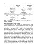
Chapter 2 Epitaxial Silicon Solar Cells 29
Vasiliki Perraki
Chapter 3 A New Model for Extracting the Physical Parameters
from I-V Curves of Organic and Inorganic Solar Cells 53
N. Nehaoua, Y. Chergui and D. E. Mekki
Chapter 4 Trichromatic High Resolution-LBIC: A System for
the Micrometric Characterization of Solar Cells 67
Javier Navas, Rodrigo Alcántara, Concha Fernández-Lorenzo
and Joaquín Martín-Calleja
Chapter 5 Silicon Solar Cells:
Structural Properties of Ag-Contacts/Si-Substrate 93
Ching-Hsi Lin, Shih-Peng Hsu and Wei-Chih Hsu
Chapter 6 Possibilities of Usage LBIC Method
for Characterisation of Solar Cells 111
Jiri Vanek and Kristyna Jandova
Chapter 7 Producing Poly-Silicon from Silane
in a Fluidized Bed Reactor 125
B. Erik Ydstie and Juan Du
Chapter 8 Silicon-Based Third Generation Photovoltaics 139
Tetyana Nychyporuk and Mustapha Lemiti
Chapter 9 Optical Insights into Enhancement of Solar
Cell Performance Based on Porous Silicon Surfaces 179
Asmiet Ramizy, Y. Al-Douri, Khalid Omar and Z. Hassan
VI Contents
Chapter 10 Evaluation the Accuracy of One-Diode and
Two-Diode Models for a Solar Panel Based
Open-Air Climate Measurements 201
Mohsen Taherbaneh, Gholamreza Farahani and Karim Rahmani
Chapter 11 Non-Idealities in the I-V Characteristic of the PV Generators:
Manufacturing Mismatch and Shading Effect 229
Filippo Spertino, Paolo Di Leo and Fabio Corona
Chapter 12 Light Trapping Design in Silicon-Based Solar Cells 255
Fengxiang Chen and Lisheng Wang
Chapter 13 Characterization of Thin Films for Solar Cells
and Photodetectors and Possibilities
for Improvement of Solar Cells Characteristics 275
Aleksandra Vasic, Milos Vujisic,
Koviljka Stankovic and Predrag Osmokrovic
Chapter 14 Solar Cells on the Base
of Semiconductor-Insulator-Semiconductor Structures 299
Alexei Simaschevici, Dormidont Serban and Leonid Bruc
Chapter 15 Maturity of Photovoltaic Solar-Energy Conversion 333
Michael Y. Levy
Chapter 16 Application of the Genetic Algorithms for Identifying
the Electrical Parameters of PV Solar Generators 349
Anis Sellami
and Mongi Bouaïcha
Preface
The third book of four-volume edition of “Solar Cells” is devoted to solar cells based on
silicon wafers, i.e., the main material used in today's photovoltaics. Single-crystalline Si
(c-Si) modules are among the most efficient but at the same time the most expensive
since they require the highest purity silicon and involve a lot of stages of complicated
processes in their manufacture. Polycrystalline silicon (mc-Si) cells are less expensive to
produce solar cells but are less efficient. As a result, cost per unit of generated electric
power for c-Si and mc-Si modules is practically equal. Nevertheless, wafer silicon
technology provides a fairly high rate of development of solar energy. Photovoltaics of
all types on silicon wafers (ribbons), representatives of the so-called first generation
photovoltaics, will retain their market position in the future. In hundreds of companies
around the world, one can always invest with minimal risk and implement the silicon
technology developed for microelectronics with some minor modifications.
For decades, an intensive search for cheaper production technology of silicon wafer-
based solar cells is underway. The results of research and development, carried out for
this purpose, lead to positive results although too slowly. This book includes the
chapters that present new results of research aimed to improve efficiency, to reduce
consumption of materials and to lower the cost of wafer-based silicon solar cells as
well as new methods of research and testing of the devices contributing to the
achievement of this goal. Light trapping design in c-Si and mc-Si solar cells, solar-
energy conversion as a function of the geometric-concentration factor, design criteria
for spacecraft solar arrays are considered in several chapters. A system for extracting
the physical parameters from I-V curves of solar cells and PV solar generators, the
micrometric characterization of solar cells, LBIC method for characterization of solar
cells, and a new model for non-idealities in the I-V characteristic of the PV generators
are discussed in other chapters of the volume.
It is hoped that this volume of “Solar Cells” will be of interest for many readers.
The editor addresses special thanks to the contributors for their initiative and high
quality work, and to the technical editors that conveyed the text into a qualitative and
pleasant presentation.
Professor, Doctor of Sciences, Leonid A. Kosyachenko
National University of Chernivtsi
Ukraine
1
Solar Cell
Purnomo Sidi Priambodo, Nji Raden Poespawati and Djoko Hartanto
Universitas Indonesia
Indonesia
1. Introduction
Solar cell is the most potential energy source for the future, due to its characteristics of
renewable and pollution free. However, the recent technology still does not achieve high
Watt/m
2
and cost efficiency. Solar cell technology still needs to be developed and improved
further to obtain optimal efficiency and cost. Moreover, in order to analyze and develop the
solar cell technologies, it is required the understanding of solar cell fundamental concepts.
The fundamentals how the solar works include 2 phenomena, i.e.: (1) Photonics electron
excitation effect to generate electron-hole pairs in materials and (2) diode rectifying.
The phenomenon of photonics electron excitation is general nature evidence in any
materials which absorbs photonic energy, where the photonic wavelength corresponds to
energy that sufficient to excite the external orbit electrons in the bulk material. The
excitation process generates electron-hole pairs which each own quantum momentum
corresponds to the absorbed energy. Naturally, the separated electron and hole will be
recombined with other electron-holes in the bulk material. When the recombination is
occurred, it means there is no conversion energy from photonics energy to electrical energy,
because there is no external electrical load can utilize this natural recombination energy.
To utilize the energy conversion from photonic to electric, the energy conversion process
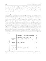
should not be conducted in a bulk material, however, it must be conducted in a device
which has rectifying function. The device with rectifying function in electronics is called
diode. Inside diode device, which is illuminated and excited by incoming light, the electron-
hole pairs are generated in p and n-parts of the p-n diode. The generated pairs are not
instantly recombined in the surrounding exciting local area. However, due to rectifying
function, holes will flow through p-part to the external electrical load, while the excited
electron will flow through n-part to the external electrical load. Recombination process of
generated electron-hole pairs ideally occurs after the generated electrons-holes experience
energy degradation after passing through the external load outside of the diode device, such
as shown in illustration on Figure-1.
The conventional structure of p-n diode is made by crystalline semiconductor materials of
Group IV consists of silicon (Si) and germanium (Ge). As an illustration in this discussion, Si
diode is used, as shown in Figure-1 above, the sun light impinges on the Si p-n diode,
wavelengths shorter than the wavelength of Si bandgap energy, will be absorbed by the Si
material of the diode, and exciting the external orbit electrons of the Si atoms. The electron
excitation process causes the generation of electron-hole pair. The wavelengths longer than
the wavelength of Si bandgap energy, will not be absorbed and not cause excitation process
Solar Cells – Silicon Wafer-Based Technologies
2
to generate electron-hole pair. The excitation and electron-hole pair generation processes
are engineered such that to be a useful photon to electric conversion. The fact that electron
excitation occurs on ߣ < λ
bandgap-Si
, shows the maximum limit possibility of energy
conversion from sun-light to electricity, for solar cell made based on Si.
Fig. 1. Illustration of solar cell device structure in the form of p-n diode with external load.
The holes flow to the left through the valanche band of diode p-part and the electrons flow
through the conduction band of diode n-part.
The fundamental structure of solar cell diode does not change. The researchers have made
abundance engineering experiment to improve efficiency by involving many different
materials and alloys and also restructuring the solar cell fundamental structure for the
following reasons:
1. Energy conversion efficiency Watt/m2 improvement from photon to electricity.
2. Utilization of lower cost material that large availability in nature
3. Utilization of recyclable materials
4. The simplification of fabrication process and less waste materials
5. Longer solar cell life time
In this Chapter, we will discuss several topics, such as: (1) Solar cell device in an ideal diode
perspective; (2) Engineering methods to improve conversion energy efficiency per unit area
by involving device-structure engineering and material alloys; (3) Standar solar cell
fabrications and (4) Dye-sensitized solar cell (DSSC) as an alternative for inexpenssive
technology.
2. Solar cell device in an ideal diode perspective
In order to be able to analyze further the solar cell performance, we need to understand the
concepts of an ideal diode, as discussed in the following explanation. In general, an ideal
diode with no illumination of light, will have a dark I-V equation as following
[1]
:
Solar Cell
3
/
0
1
B
qV k T
IIe
(1)
where I is current through the diode at forward or reverse bias condition. While, I
0
is a well
known diode saturation current at reverse bias condition. T is an absolute temperature
o
K, k
B
is Boltzmann constant, q (> 0) is an electron charge and V is the voltage between two
terminals of p-n ideal diode. The current capacity of the diode can be controlled by
designing the diode saturation current I
0
parameter, which is governed by the following
equation
[1]
:
22
0
ei hi
eA hD
Dn Dn
IqA
LN LN
(2)
where
A is cross-section area of the diode, n
i
is concentration or number of intrinsic electron-
hole pair /cm
3
, D
e
is the diffusion coefficient of negative (electron) charge, D
h
is the
diffusion coefficient of positive (hole) charge,
L
e
and L
h
are minority carrier diffusion
lengths, N
A
is the extrinsic acceptor concentration at p-diode side and N
D
is the extrinsic
donor concentration at
n-diode side
[1]
.
eee
LD
dan
hhh
LD
(3)
where
τ
e
and τ
h
are minority carrier lifetime constants, which depend on the material types
used. From Equations (2) & (3) above, it is clearly shown that the diode saturation current I
0
is very depended on the structure and materials of the diode. The I-V relationship of a dark
condition is shown on Figure-2.
Fig. 2. I-V relationship of ideal diode for dark or no illumination. (a) I-V graph and (b) the
equivalent ideal diode circuit.
Solar Cells – Silicon Wafer-Based Technologies
4
Furthermore, if an ideal diode is designed as a solar cell, when illuminated by sun-light,
there will be an energy conversion from photon to electricity as illustrated by a circuit model
shown on Figure-3. As already explained on Figure-1 that the electron excitation caused by
photon energy from the sun, will corresponds to generation of electron-hole pair, which
electron and hole are flowing through their own bands. The excited electron flow will be
recombined with the hole flow after the energy reduced due to absortion by the external
load.
The circuit model of Figure-3, shows a condition when an ideal diode illuminated, the ideal
diode becomes a current source with an external load having a voltage drop V. The total
output current, which is a form of energy conversion from illumination photon to electricity,
is represented in the form of superposition of currents, which are resulted due to photon
illumination and forward current bias caused by positive voltage across
p and n terminals.
The corresponding
I-V characteristic of an ideal diode solar cell is described by the Shockley
solar cell equation as follows
[3]
:
/
0
1
B
qV k T
photon
II Ie
(4)
p
hoton
I
is the photogenerated current, closely related to the photon flux incident to the solar
cell. In general,
p
hoton
I
can be written in the following formula
[2]
p
hoton e h
I
q
AG L W L
(5)
where G is the electron-hole pair generation rate of the diode, W is depletion region width of
the solar cell diode. The
G value absolutely depends on material types used for the device
and the illumination spectrum and intensity (see Eq 14a & b), while W value depends on the
device structure, A is the cross-section of illuminated area. The I-V characteristic of an ideal
diode solar cell is illustrated in Figure-4.
Fig. 3. The equivalent circuit model of an ideal diode solar cell.
Solar Cell
5
Fig. 4. The Graph of the I-V characteristics of an ideal diode solar cell when non-illuminated
(dark) and illuminated.
Solar cell output parameters
From Figure-4, it is shown that there are 4 output parameters, which have to be considered
in solar cell. The first parameter is
I
SC
that is short circuit current output of solar cell, which
is measured when the output terminal is shorted or
V is equal to 0. The value of output
current
I = I
SC
=
p
hoton
I
represents the current delivery capacity of solar cell at a certain
illumination level and is represented by Equation (4). The second parameter is
V
OC
that is
the open circuit output voltage of solar cell, which is measured when the output terminal is
opened or
I is equal to 0. The value of output voltage V
OC
represents the maximum output
voltage of solar cell at a certain illumination level and can be derived from Equation (4) with
output current value
setting at I = 0, as follows:
0
ln 1
photon
B
OC
I
kT
V
qI
(6)
In general, V
OC
is determined by I
photon
, I
0
and temperature, where I
0
absolutely depends on
the structure design and the choice of materials for solar cell diode, while I
photon
besides
depending on the structure design and the choice of materials, depends on the illumination
intensity as well.
The maximum delivery output power is represented by the area of product V
MP
by I
MP
as
the maximum possible area at fourth quadrant of Figure-4.
M
PMPMP
PVI
(7)
The third parameter is fill factor FF that represents the ratio PMP to the product V
OC
and I
SC
.
This parameter gives an insight about how “square” is the output characteristic.
Solar Cells – Silicon Wafer-Based Technologies
6
M
PMPMP
OC SC OC SC
PVI
FF
VI VI
(8)
In the case of solar cell with sufficient efficiency, in general, it has FF between 0.7 and 0.85.
The energy –conversion efficiency, η as the fourth parameter can be written as
[2]
MP MP OC SC
in in
VI VIFF
PP
(9)
where P
in
is the total power of light illumination on the cell. Energy-conversion efficiency of
commercial solar cells typically lies between 12 and 14 %
[2]
. In designing a good solar cell,
we have to consider and put any effort to make those four parameters I
SC
, V
OC
, FF and η as
optimum as possible. We like to use term optimum than maximum, since the effort to obtain
one parameter maximum in designing solar cell, will degrade other parameters. Hence the
best is considering the optimum efficiency of solar cell.
3. Improvement of solar cell performance
In the process to improve solar cell output performance that is energy conversion efficiency
from photon to electricity, which is typically lies between 12 to 14 %
[2]
, the researchers have
been conducting many efforts which can be categorized and focused on:
1.
Diode device structure engineering to improve current output I
sc
, by reducing I
0
and
increasing photon illumination conversion to I
photon
in the form of improving G
parameter, electron-hole pair generation constant. The diode structure engineering, at
the same time also improving output voltage in the form of V
OC
, and improving FF and
finally improving the energy conversion efficiency from photon to electricity.
2.
Material engineering, especially to obtain improvement on G parameter, electron-hole
pair generation.
3.
Device structure engineering to improve quantum efficiency and lowering top-surface
lateral current flow to reduce internal resistance.
4.
Solar cell structure engineering includes concentrating photon energy to the solar cell
device.
3.1 Solar cell diode structure engineering
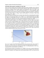
In general, sun-light illuminates solar cell with the direction as shown on Figure-5.
The light illumination with λ > λ
bandgap
will pass through without absorbed by solar cell.
While the light with λ < λ
bandgap
will be absorbed. Whatever spectrum, basically, incident
light with λ < λ
bandgap
will be absorbed as a function of exponential decay with respect to
distance parameter as
()z
e
from the top surface, where α(λ) is absorption coefficient and z
is the depth distance in the solar cell diode. Absorption occurs at any absorbed wavelength
are shown on Figure-6.
As shown on Figure-6, red light will be absorbed exponentially slower than the blue light.
The photons with different wavelengths will be absorbed in different speed. This
discrepancy can be explained and derived by using the probability of state occupancies in
material, which is illustrated by Fermi function as follows
[1]
:
1
()
exp / 1
fB
fE
EE kT
(10)
Solar Cell
7
Fig. 5. A generic solar cell diode structure and the incidence light direction
Fig. 6. A normalized hole-electron pair generation rate
[2]
.
when
exp / 1
fB
EE kT
, then Equation (10) can be written as
/
() e
fB
EE kT
fE
(11)
where E represents the energy state in crystalline. Moreover, photon absorption α(λ) by
material is an equal representation of excitation probability of electron leaving hole towards
a state in conduction band after excited by a photon. The probability is the integral
accumulation of multiplication between electron occupation probability in valence band
Solar Cells – Silicon Wafer-Based Technologies
8
and probability of possible state that can be occupied by the excited electron, furthermore
those two are multiplied by a coefficient σ(λ) as shown in the following equation:
() ()(1 ( ))
v
c
E
hc
E
hc
f
EfE dE
(12)
where σ(λ) is a cross section probability parameter represent of possible occurrence the
photon to hole-electron pair generation at wavelength λ. Parameter σ(λ) is obtained by the
following derivation
[2]
:
22
//
()
exp( / ) 1 1 exp( / )
gp gp
pB pB
hc E E hc E E
D
EkT EkT
(13)
where parameters D, Eg and Ep depend on material types used and crystalline quality, and
usually are obtained by conducting experiments. Eg and Ep each are bandgap energy dan
phonon absorption or emission energy respectively, h is the Plank constant and c is the light
speed in vacuum. The σ(λ) parameter is a function of λ and naturally depends on the type of
the material. Parameter absorption α(λ) on Equation (12) when multiplied by illumination
intensity I
int
(λ), will represent the generation rate of hole-electron pairs at λ or G(λ).
int int
() () () () ()(1 ( ))
v
c
E
hc
E
hc
GI I
f
E
f
EdE
(14-a)
Furthermore, the generation rate of hole-electron pair G can be written as the integral of G(λ)
as following:
0
bandgap
GGd
(14-b)
In a glance, the terms multiplication under the integral and the integral limits of Equations
(12 and 14a) show that parameter values G(λ) or α(λ) getting larger for
becoming shorter
(agrees to Figure-6). λ
bandgap
is the
of the bandgap energy as the limit of irradiance photon
to electric conversion. At λ > λ
bandgap
, σ(λ) is zero and will not be absorbed or there is no
electron-hole generation and does not contribute to the conversion. The following Figure-7
illustrates the distribution state of a material with respect to the Fermi function. The
transition state probability represents the photon to hole-electron pair generation.
Back to Figure-5, naturally layer n
+
is a layer that more easier to generate hole-electron pairs
due to photon excitation, in comparison to layer p
+
. Hence, the n
+
layer is called as an
electron emitter layer. By considering Figure-5 and 6 that photon absorption and hole-
electron generation occurs at the front layer of diode structure, then in order to obtain
higher conversion efficiency, the n
+
layer as electron emitter layer is located on the top
surface of solar cell diode structure such as shown on Figure-5 above.
However, in order to be an effective electron emitter layer, the thickness of the n
+
layer must
be shorter than the minority carrier diffusion length L
h
in n
+
layer, where the hole minority
Solar Cell
9
Fig. 7. Transition state probability illustration
[4]
.
carrier diffusion lengths L
h
is governed by Equation (3). If the thickness of n
+
layer > L
h
,
then most of hole-electron pairs experience local recombination, which means useless for
photon to electrical energy conversion. Between n
+
and p
+
layers, there exists a depletion
layer, which has a built in potential V
bi
to conduct collection probability of the generated
hole-electron pairs. The width of depletion layer can be written as follows
[1]
:
1/2
0
2
r
AD
bi A
AD
NN
WVV
qNN
(15)
where W is the depletion layer width, V
bi
is the diode built in potential and V
A
is the
applied or solar cell output voltage. The diode built in potential can be approach by the
following Equation
[1]
:
2
ln
BAD
bi
i
kT N N
V
q
n
(16)
The collection probability describes the probability that the light absorbed in a certain region
of the device will generate hole-electron pairs which will be collected by depletion layer at
p-n junction. The collected charges contribute to the output current
p
hoton
I
. However, the
probability depends on the distance to the junction compared to the diffusion length. If the
distance is longer than the diffusion length, then instead of contributing to the output
current, those hole-electron pairs are locally recombined again, hence the collection
probability is very low. The collection probability is normally high (normalized to 1) at the
depletion layer. The following Figure-8 shows the occurrence of photon absorption by the
device that illustrated as an exponential decay, at the same time, representing generation of
hole-electron pairs. The collection probability shows that at the front (top) surface is low
Solar Cells – Silicon Wafer-Based Technologies
10
because far from the built-in voltage at depletion layer. On depletion layer, collection
probability very high and give a large contribution on output current
p
hoton
I
.
Fig. 8. The collection probability of the generated hole-electron pairs at junction
[5]
.
As explained previously, there are 4 reference parameters in designing solar cell, i.e.: I
sc
,
V
OC
, FF and η. By considering the equations of those 4 parameters, it is likely that the four
parameters are correlated each other. For instance, in order to increase I
sc
or
p
hoton
I
(1
st
parameter), we have to consider Equation (5), where the structure will depend on 2
parameters i.e. A the area of the cell surface and W the thickness of the depletion layer.
While parameters G, L
e
and L
h
depend on the materials used for the solar cell diode.
Increasing A parameter (the area of diode) will not have impact to other parameters,
however, increasing W parameter will have impact to other parameters. Of course, by
increasing A, the total output current I
photonic
will increase proportionally, the increasing W,
the length of collection probability of depletion layer will increase as well, where finally it is
expected to improve contribution to the output current.
From Equations [15] dan [16], it is shown that structurally W parameter depends on N
A
and
N
D
. In order to increase W proportionally linear, then what we can do is by reducing
doping concentration of N
A
and N
D
or one of both. The consequence of reducing N
A
and/or
N
D
is the linear increment of I
0
, which in the end causing reducing the total output current
such as shown in Equation (4). Don’t be panic, improvement I
SC
in one side and decreasing
in other side due to concentration adjustment of N
A
and/or N
D
does not mean there is no
meaning at all. Because at a certain N
A
and/or N
D
value +ΔI
SC
that caused by ΔW can be
much larger than -ΔI
SC
that caused by I
0
. Hence, to obtain the optimal design, it is required
to apply a comprehensive numerical calculation and analysis to obtain the optimal I
SC
.
For the sake of obtaining an optimal output voltage V
OC
(2
nd
parameter), we have to
consider Equation (6). The equation shows that V
OC
is a natural logarithmic function of
I
SC
/I
0
, it shows that by reducing N
A
and/or N
D
will cause on increasing I
SC
in root square
manner and linearly proportional to I
0
that causes decreasing of V
OC
. Hence, there is a trade
off that to increase I
SC
by structural engineering will cause to decrease V
OC
. At certain level,
the improvement of I
SC
can be much higher compared to the decrease of V
OC
. Therefore,
again, to obtain an optimal design, it is required to apply a comprehensive numerical
calculation and analysis to obtain the optimal I
SC
, V
OC
and output power.
Solar Cell
11
The third parameter is fill factor FF, which is a measure on how “square” is the output
characteristic of solar cell. It is shown by the curve in the 4
th
quadrant of I-V graph in Figure-
4. The shape of the curve is governed by Equation (4). It means FF is low for very large I
0
.
The fourth parameter η, as shown in Equation (9), linearly depends on the other three
parameters. Here, we can conclude that in term of structure design, increasing one of the
parameter, for instance I
SC
will cause reduction on other parameters, for example V
OC
, and
so vice versa. Finally, it is concluded that it is required to compromise between thus four
output parameters to obtain the optimal condition.
When the optimalization process of four parameters from the structure given on Figure-5 is
conducted by reducing the dopant concentration of one part (in general is p), then the solar
cell will experience and have a relatively high internal resistance, which reducing output the
performance parameter η. Hence, the structure in Figure-5 should be modified by inserting a
layer that has a lower dopant concentration as shown in the following Figure-9, and keep
the higher dopant concentration layers for ohmic contacts at the top and bottom contacts. By
inserting layer p in between layer p
+
dan n
+
will cause the contact p to the contact + will have
a low internal resistance, as same as between n
+
to contact
Fig. 9. Insertion of a lower dopant layer p in p-n junction diode to improve collection
probability area and keep solar cell internal resistance lower.
1
st
generation of solar cells
1
st
generation of solar cell is indicated by the usage of material, which is based on silicon
crystalline (c-Si). Typically solar cell is made from a single crystal silicon wafer (c-Si), with a
simple p
+
-p-n
+
juction diode structure (Figure-9) in large area, with bandgap energy 1.11 eV.
In the development process, the usage of c-Si causes the price of solar cell very high, hence
emerging the idea to use non-crystalline or poly-crystalline Si for producing solar cells.
There was compromising between cost and efficiency. Using poly-crystalline material the
price is cut down to the lower one since the fabrication cost is much lower, however the
efficiency is going down as well, since the minority carrier lifetimes τ
e
and τ
h
are shorter in
poly-crystalline than in single–crystalline Si that makes lower I
photon
(Equations (3 - 5)). For
the ground application with no limitation of area, it is considered to use lower price solar
cells with lower conversion efficiency. However, for application with limited areas for
Solar Cells – Silicon Wafer-Based Technologies
12
instances on high-rise buildings and even on satellites, space shuttles or space-lab, a higher
conversion efficiency is much considered. The first generation of solar cells based on poly-
crystalline Si still dominates the market nowadays. The conversion energy efficiency
typically reaches 12 to 14 %.
3.2 Material engineering to improve conversion parameter G (electron-hole pair
generation rate)
2
nd
generation of solar cells
Instead of based on traditional Si wafer cystalline and polycrystalline, in the 2
nd
Generation
solar cell, it began to use material alloys such as elemental group IV alloy for instance SiGe
(silicon-germanium), binary and ternary III-V group alloy for instances InGaP, GaAs and
AlGaAs. Futhermore, binary to quaternary II-VI group alloy is used as well, such as
Cadmium Telluride (CdTe) and Copper Indium Galium Diselenide (CIGS) alloys. The goals
of using such material alloys in solar cell diode structure is to improve the irradiance photon
to electric conversion rate parameter G such as shown in Equation (5) and has been derived
in Equations (14-a and b).
By common sense, if λ
bandgap
is as large as possible, then we can expect that the G parameter
goes up. This is the reason, why one applies SiGe for the solar cell, since the alloy has lower
bandgap than Si, where the bandgap energy is governed by the following formula
[6]
where
x represents the percent composition of Germanium:
E
g
(x)= (1.155 – 0.43x + 0.0206x
2
)eV for 0 < x < 0.85 (17)
and
E
g
(x)= (2.010 – 1.27x)eV for 0.85 < x < 1 (18)
The usage of SiGe alloy for solar cell results in the improvement of conversion efficiency up
to 18%
[11]
.
Multi-junction solar cells
In the first generation, Solar cell diode structure used a single type material Si in the form of
crystalline, poly-crystalline and amorphous. In the development of 2
nd
generation solar cell,
the researchers use several material alloys in one single device, then it is called as multi-
junction solar cell. As already explained and illustrated in Figure-6 that the shorter the
photonic wavelength then it will be absorbed faster inside the material. It means the shorter
wavelength part of the sun light spectrum will be absorbed more than the longer part of the
spectrum by the same thickness of material. The wavelengths longer than the bandgap
wavelength will not be absorbed at all. The part of the spectrum not absorbed by the diode
material is the inefficiency of the solar cell. In order to improve solar cell efficiency
performance, then the remaining unabsorbed spectrum must be reabsorbed by the next
structure that can converting become electricity. The solar cell structures in the second
generation are mostly in the form of tandem structure, which consists of various alloy
materials that have different bandgaps with sequence from the top surface, is the highest
bandgap then continued by the lower and finaly the lowest, such as illustrated on Figure-10.
There may be a question, if the lower bandgap can absorb more spectrum, why not it is used
a single diode structure with very low bandgap material to absorb the overall spectrum
energy? without building tandem or cascading structures. The answer is following, it is
Solar Cell
13
correct that more lower the bandgap energy; the material can be categorized as more
effective in photon absorption. Hence, for photons with the same wavelength will be absorb
faster in lower bandgap typed material in comparison to the larger bandgap material. Thus
mechanism is very clear illustrated in math relation by Equations (12 and 14a).
Fig. 10. Multi-junction and cell tandem concept.
The higher energy photon will be very fast absorbed and then generate hole-electron pairs
with a high concentration in area close to the top surface of diode, which naturally has
abundance surface defects corresponds to deep level trap close the surface. This surface
defects cause a fast recombination process. Hence, it can be concluded that the usage of one
diode structure with a lower bandgap energy, then a wide photon spectrum can be
absorbed, however, the generated electron-hole pairs by the high energy photon will be
recombined because located near the surface area with abundance defects and deep level
states. Therefore, to make effective absorption and efficient conversion, the solar cell should
be in the tandem structure such as illustrated in Figure-10. Further, Figure-11 shows a
typical design of multi-junction or tandem solar cell incorporating III-V group of materials.
While the first generation with 12 to 14% efficiency dominates the market nowadays, this
second generation of solar cells based on multi-junction structure dominates the market of
high efficient solar cell as well, which typically reach 35 to 47 % efficiency. The typical
applications of high efficient second generation solar cell with multi-junction technology are
for satellite communications and space shuttles. To design multi-junction structure, it is
required to have a knowledge about crystalline lattice match. If the crystalline lattice does
not match, then there will exist abundance of deep level states in the junction region that
cause a short carrier life-time or it causes faster or larger local recombination process. This
large local recombination, finally will reduce the output current I
photon
. The information
regarding to the bandgap energies dan lattice match of various material are shown on
Figures-12 and 13
[4]
as follows.
Thus two first generations, besides of dominating solar cell technologies and markets
nowadays, also are dominated by the usage of mostly silicon alloy based on semiconductor
material. This situation causes the ratio of the solar cell price to the Watt-output power
never decrease, because it tightly compete with the usage of Si and other semiconductor
Solar Cells – Silicon Wafer-Based Technologies
14
Fig. 11. Typical of high efficient solar cell with dual cell tandem structure
[12]
.
Fig. 12. Lattice constants, bandgap energies and bandgap wavelengths for III-V binary
compounds, Si and Ge
[4]
.
Solar Cell
15
material for the global electronics industry demand. The condition encourages the
researchers to create a radical technology revolution, by using non-crystalline material that
replacing Si and other semiconductor materials, and it is realized in the form of dye-
sensitized solar cell (DSSC) as the 3
rd
generation solar cells.
Fig. 13. Lattice constants, bandgap energies and bandgap wavelengths for important II-VI
binary compounds
[4]
.
3.3 Quantum efficiency engineering (optical design)
Antireflection (AR) thin-film coating
As already well understood that the sun-light before reaching solar cell, propagates through
the vacuum and air. At the moment when the light reaches the solar cell front surface, which
is made by silicon material, the light experiences of reflection by the silicon surface due to
the index of refraction difference between air and silicon. The reflection causes reduction of
overall efficiency of the solar cell. We have to reduce the reflection in order to increase the
efficiency. By borrowing the technique that has been well developed in optical science,
furthermore to reduce reflection or increase absorption, it uses antireflection thin film
coating structure applied on top of the front solar cell surface. Basically this technique uses
Bragg reflection phenomenon, that is an interference effect caused by thin film structure.
The following Figure-14 illustrates the process of Bragg reflection occurrence by the mirror
stack structure. The reflectance occurs when the light incidence on an interface of two
material with different index of refraction n
1
≠ n
2
.
The maximum reflection intensity occurs when the following condition is set and called as
Bragg angle
[4]
sin
2d
(19)
For normal incidence θ = 90
0
, with Bragg equation, distance between mirrors needed for
constructive interference reflectance is d = λ/2. While for the requirement of destructive