Solar Cells Silicon Wafer Based Technologies Part 9 potx
Bạn đang xem bản rút gọn của tài liệu. Xem và tải ngay bản đầy đủ của tài liệu tại đây (1.22 MB, 25 trang )
Optical Insights into Enhancement
of Solar Cell Performance Based on Porous Silicon Surfaces
191
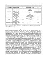
Fig. 16. Current-voltage (IV) characteristics of Si (as grown) and Si of different sides
Samples
R
s
(Ω)
R
sh
(kΩ)
V
m
(V)
I
m
(mA)
V
oc
(V)
I
sc
(mA)
FF (%)
Efficiency
(
) (%)
Si as-grown 70.4 2.98 0.26 6.71 0.31 6.72 83 4.34
PS formed on the
unpolished side
7.14 149.8 0.41 7.24 0.43 8.83 78 7.38
PS formed on both
sides
7.9 4.86 0.44 11.65 0.45 12.37 84 12.75
PS on both sides
with lens
2.81 18.77 0.41 15.12 0.49 15.5 88 15.4
Table 2. Investigated series resistance Rs, shunt resistance Rsh, maximum voltage Vm,
maximum current Im, open-circuit voltage Voc, short-circuit current Isc, FF, and efficiency
(η) of Si and PS
where R is reflectivity. The refractive index n is an important physical parameter related to
microscopic atomic interactions. Theoretically, the two different approaches in viewing this
subject are the refractive index related to density and the local polarizability of these entities
[21].
In contrast, the crystalline structure represented by a delocalized picture,
n , is closely
related to the energy band structure of the material, complicated quantum mechanical
analysis requirements, and the obtained results. Many attempts have been made to relate
Solar Cells – Silicon Wafer-Based Technologies
192
the refractive index and the energy gap Eg through simple relationships [22–27]. However,
these relationships of
n are independent of temperature and incident photon energy. Here,
the various relationships between
n and
g
E
are reviewed. Ravindra et al. [27] suggested
different relationships between the band gap and the high frequency refractive index and
presented a linear form of
n as a function of
g
E
:
g
n
E
, (2)
where α = 4.048 and β = −0.62 eV−1.
To be inspired by the simple physics of light refraction and dispersion, Herve and
Vandamme [28] proposed the empirical relation as
2
1
g
A
n
B
E
, (3)
where A = 13.6 eV and B = 3.4 eV. Ghosh et al. [29] took a different approach to the problem
by considering the band structure and quantum-dielectric formulations of Penn [30] and
Van Vechten [31]. Introducing A as the contribution from the valence electrons and B as a
constant additive to the lowest band gap Eg, the expression for the high-frequency refractive
index is written as
2
2
1
g
A
n
B
E
, (4)
where A = 25Eg + 212, B = 0.21Eg + 4.25, and (Eg+B) refers to an appropriate average energy
gap of the material. Thus, these three models of variation
n with energy gap have been
calculated. The calculated refractive indices of the end-point compounds are shown in Table 3,
with the optical dielectric constant
calculated using
2
n
[32], which is dependent on
the refractive index. In Table 1, the calculated values of
using the three models are also
investigated. Increasing the porosity percentage from 60% (front side) to 80% (back side) uses
weight measurements [33] that lead to a decreasing refractive index. As with Ghosh et al. [29],
this is more appropriate for studying porous silicon solar cell optical properties, which showed
lower reflectivity and more absorption as compared to other models.
Samples
n
Si
PS formed on the unpolished side
PS formed on the front polished
side
3.35
a
2.91
b
2.89
c
3.46
d
3.46
e
3.17
a
2.79
b
2.77
c
1.8
e
2.94
a
2.68
b
2.66
c
2.38
e
11.22
a
8.46
b
8.35
c
11.97
e
10.04
a
7.78
b
7.67
c
3.24
e
8.64
a
7.18
b
7.07
c
5.66
e
a
Ref. [27],
b
Ref. [28],
c
Ref. [29],
d
Ref. [20] exp. eusing Equation (1)
Table 3. Calculated refractive indices for Si and PS using Ravindra et al. [27], Herve and
Vandamme [28], and Ghosh et al. [29] models compared with others that corresponds to the
optical dielectric constant
Optical Insights into Enhancement
of Solar Cell Performance Based on Porous Silicon Surfaces
193
6. Ionicity character
The systematic theoretical studies of the electronic structures, optical properties, and charge
distributions have already been reported in the literature [34,35]. However, detailed
calculations on covalent and ionic bonds have not reached the same degree of a priori
completeness as what can be attained in the case of metallic properties. The difficulty in
defining the ionicity lies in transforming a qualitative or verbal concept into a quantitative,
mathematical formula. Several empirical approaches have been developed [36] in yielding
analytic results that can be used for exploring the trends in materials properties. In many
applications, these empirical approaches do not give highly accurate results for each specific
material; however, they still can be very useful. The stimulating assumption of Phillips [36]
concerning the relationship of the macroscopic (dielectric constant, structure) and the
microscopic (band gap, covalent, and atomic charge densities) characteristics of a covalent
crystal is based essentially on the isotropic model of a covalent semiconductor, whereas
Christensen et al. [37] performed self-consistent calculations and used model potentials
derived from a realistic GaAs potential where additional external potentials were added to
the anion and cation sites. However, in general, the ionicities found by Christensen et al.
tend to be somewhat larger than those found by Phillips. In addition, Garcia and Cohen [38]
achieved the mapping of the ionicity scale by an unambiguous procedure based on the
measure of the asymmetry of the first principle valence charge distribution [39]. As for the
Christensen scale, their results were somewhat larger than those of the Phillips scale. Zaoui
et al. [40] established an empirical formula for the calculation of ionicity based on the
measure of the asymmetry of the total valence charge density, and their results are in
agreement with those of the Phillips scale. In the present work, the ionicity, fi, was
calculated using different formulas [41], and the theory yielded formulas with three
attractive features. Only the energy gap EgΓX was required as the input, the computation of
fi itself was trivial, and the accuracy of the results reached that of ab initio calculations. This
option is attractive because it considers the hypothetical structure and simulation of
experimental conditions that are difficult to achieve in the laboratory (e.g., very high
pressure). The goal of the current study is to understand how qualitative concepts, such as
ionicity, can be related to energy gap EgΓX with respect to the nearest-neighbor distance, d,
cohesive energy, E
coh
, and refractive index, n
0
. Our calculations are based on the energy gap
EgΓX reported previously [34,42–45], and the energy gap that follows chemical trends is
described by a homopolar energy gap. Numerous attempts have been made to face the
differences between energy levels. Empirical pseudopotential methods based on optical
spectra encountered the same problems using an elaborate (but not necessarily more
accurate) study based on one-electron atomic or crystal potential. As mentioned earlier, d,
E
coh
, and n
0
have been reported elsewhere for Si and PS. One reason for presenting these
data in the present work is that the validity of our calculations, in principle, is not restricted
in space. Thus, they will no doubt prove valuable for future work in this field. An important
observation for studying ionicity,
i
f
, is the distinguished difference between the values of
the energy gaps of the semiconductors, EgΓX, as seen in Table 2; hence, the energy gaps
EgΓX are predominantly dependent on fi . The differences between the energy gaps Egrx
have led us to consider these models, and the bases of our models are the energy gaps,
EgΓX, as seen in Table 4. The fitting of these data gives the following empirical formulas
[41]:
Solar Cells – Silicon Wafer-Based Technologies
194
/
4
gX
i
d
E
f
(5)
/
2
coh g X
i
EE
f
(6)
0
/
4
gX
i
n
E
f
(7)
where EgΓX is the energy gap in (eV), d the nearest-neighbor distance in (Å), E
coh
the
cohesive energy in (eV), n
0
the refractive index, and λ is a parameter separating the
strongly ionic materials from the weakly ionic ones. Thus, λ = 0, 1, and 6 are for the
Groups IV, III–V, and II–VI semiconductors, respectively. The calculated ionicity values
compared with those of Phillips [36], Christensen et al. [37], Garcia and Cohen [38], and
Zaoui et al. [40] are given in Table 2. We may conclude that the present ionicities, which
were calculated differently than in the definition of Phillips, are in good agreement with
the empirical ionicity values, and exhibit the same chemical trends as those found in the
values derived from the Phillips theory or those of Christensen et al. [37], Garcia and
Cohen [38], and Zaoui et al. [40] (Table 2).
Samples
d
a
(Å)
E
coh
b
(eV)
n
0
ƒ
i
cal.
ƒ
i
g
ƒ
i
h
ƒ
i
i
ƒ
i
j
E
g
ΓX
(eV)
Si 2.35 2.32 3.673
c
0
e
0
f
0 0 0 0 1.1
PS formed
on the
unpolished
side
2.77
d
0 0 0 0 0 1.82
PS formed
on the front
polished
side
2.66
d
0 0 0 0 0 1.86
a
Ref. [46],
b
Ref. [47],
c
Ref. [48],
d
Ref. [29],
e
Ref. [41]: Formulas (5–7),
f
Ref. [49],
g
Ref. [36],
h
Ref. [37],
i
Ref. [38],
j
Ref. [40]
Table 4. Calculated ionicity character for Si and PS along with those of Phillips [36],
Christensen et al. [37], Garcia and Cohen [38], Zaoui et al. [40], and Al-Douri et al. [41]
Optical Insights into Enhancement
of Solar Cell Performance Based on Porous Silicon Surfaces
195
The difficulty involved with such calculations resides with the lack of a theoretical
framework that can describe the physical properties of crystals. Generally speaking, any
definition of ionicity is likely to be imperfect. Although we may argue that, for many of
these compounds, the empirically calculated differences are of the same order as the
differences between the reported measured values, these trends are still expected to be real
[47]. The unchanged ionicity characters of bulk Si and PS are noticed. In conclusion, the
empirical models obtained for the ionicity give results in good agreement with the results of
other scales, which in turn demonstrate the validity of our models to predict some other
physical properties of such compounds.
7. Material stiffness
The bulk modulus is known as a reflectance of the crucial material stiffness in different
industries. Many authors [50–55] have made various efforts to explore the thermodynamic
properties of solids, particularly in examining the thermodynamic properties such as the
inter-atomic separation and the bulk modulus of solids with different approximations and
best-fit relations [52–55]. Computing the important number of structural and electronic
properties of solids with great accuracy has now become possible, even though the ab initio
calculations are complex and require significant effort. Therefore, additional empirical
approaches have been developed [36, 47] to compute properties of materials. In many cases,
the empirical methods offer the advantage of applicability to a broad class of materials and
to illustrate trends. In many applications, these empirical approaches do not provide highly
accurate results for each specific material; however, they are still very useful. Cohen [46]
established an empirical formula for calculating bulk modulus B0 based on the nearest-
neighbor distance, and the result is in agreement with the experimental values. Lam et al.
[56] derived an analytical expression for the bulk modulus from the total energy that gives
similar numerical results even though this expression is different in structure from the
empirical formula. Furthermore, they obtained an analytical expression for the pressure
derivative B0 of the bulk modulus. Meanwhile, our group [57] used a concept based on the
energy gap along Γ-X and transition pressure to establish an empirical formula for the
calculation of the bulk modulus, the results of which are in good agreement with the
experimental data and other calculations. In the present work, we have established an
empirical formula for the calculation of bulk modulus B0 of a specific class of materials, and
the theory yielded a formula with three attractive features. Apparently, only the energy gap
along Γ -X and transition pressure are required as an input, and the computation of B0 in
itself is trivial. The consideration of the hypothetical structure and simulation of the
experimental conditions are required to make practical use of this formula.
The aim of the present study is to determine how a qualitative concept, such as the bulk
modulus, can be related to the energy gap. We [57] obtained a simple formula for the bulk
moduli of diamond and zinc-blende solids using scaling arguments for the relevant bonding
and volume. The dominant effect in these materials has been argued to be the degree of
covalence, as characterized by the homopolar gap, Eh of Phillips, [36] and the gap along Γ-X
[57]. Our calculation is based upon the energy gap along Γ-X which has been reported
previously [42–45], and the energy gaps that follow chemical trends are described by
homopolar and heteropolar energy gaps. Empirical pseudopotential methods based on
Solar Cells – Silicon Wafer-Based Technologies
196
optical spectra encounter the same problems using an elaborate (but not necessarily more
accurate) study based on one electron atomic or crystal potential. One of the earliest
approaches [58] involved in correlating the transition pressure with the optical band gap
[e.g., the band gap for α-Sn is zero and the pressure for a transition to β-Sn is vanishingly
small, whereas for Si with a band gap of 1 eV, the pressure for the same transition is
approximately 12.5 GPa (125 kbar)]. A more recent effort is from Van Vechten [59], who
used the dielectric theory of Phillips [36] to scale the zinc-blende to β-Sn transition with the
ionic and covalent components of the chemical bond. The theory is a considerable
improvement with respect to earlier efforts, but is limited to the zinc-blende to β-Sn
transition. As mentioned, EgΓX and Pt have been reported elsewhere for several
semiconducting compounds. One reason for presenting these data in the current work is
that the validity of our calculations is not restricted in computed space. Thus, the data is
bound prove valuable for future work in this field.
An important reason for studying B0 is the observation of clear differences between the
energy gap along Γ-X in going from the group IV, III–V, and II–VI semiconductors in
Table 4, where one can see the effect of the increasing covalence. As covalence increases,
the pseudopotential becomes more attractive and pulls the charge more toward the core
region, thereby reducing the number of electrons available for bonding. The modulus
generally increases with the increasing covalence, but not as quickly as predicted by the
uniform density term. Hence, the energy gaps are predominantly dependent on B0. A
likely origin for the above result is the increase of ionicity and the loss of covalence. The
effect of ionicity reduces the amount of bonding charge and the bulk modulus. This
picture is essentially consistent with the present results; hence, the ionic contribution to
B0 is of the order 40%–50% smaller. The differences between the energy gaps have led us
to consider this model.
The basis of our model is the energy gap as seen in Table 4. The fitting of these data gives
the following empirical formula [57]:
1/2
0
30 10 / /3
gX
t
BPE
(8)
where EgΓX is the energy gap along Γ-X (in eV), Pt is the transition pressure (in GPa
‘‘kbar’’), and λ is an empirical parameter that accounts for the effect of ionicity; λ = 0; 1, 5 for
group IV, III–V, and II–VI semiconductors, respectively. In Table 5, the calculated bulk
modulus values are compared with the experimental values and the results of Cohen [46],
Lam et al. [56], and Al-Douri et al. [57].
We may conclude that the present bulk moduli calculated in a different way than in the
definition of Cohen are in good agreement with the experimental values. Furthermore, the
moduli exhibit the same chemical trends as those found for the values derived from the
experimental values, as seen in Table 5. The results of our calculations are in reasonable
agreement with the results of Cohen [46] and the experiments of Lam et al. [56], and are
more accurate than in our previous work [57]. As mentioned previously, an approach [57]
that elucidates the correlation of the transition pressure with the optical band gap exists.
This procedure gives a rough correlation and fails badly for some materials such as AlSb
that have a larger band gap than Si but have a lower transition pressure [64]. From the
above empirical formula, a correlation is evident between the transition pressure and B0
Optical Insights into Enhancement
of Solar Cell Performance Based on Porous Silicon Surfaces
197
[e.g., the B
0
for Si is 100.7 GPa and the pressure for the transition to β-Sn is 12.5 GPa (125
kbar), whereas for GaSb, B0 is 55.5 GPa and the transition pressure to β-Sn is 7.65 GPa
(76.5 kbar)]. This correlation fails for a compound such as ZnS that has a smaller value of
B0 than Si but has a larger transition pressure. In conclusion, the empirical model
obtained for the bulk modulus gives results that are in good overall agreement with
previous results.
Samples
B
0
cal.
(GPa)
B
0
exp.
b
(GPa)
B
0
[46]
(GPa)
B
0
[56]
(GPa)
B
0
[57]
(GPa)
B
0
(GPa)
P
t
e
(GPa)
Si
101
a’
91.5
a’’
100
a’’’
98 98 100 92
92
c
93.6
d
12.5
PS formed
on the
unpolished
side
61.4
a’
150.7
a’’
165
a’’’
PS formed
on the front
polished
side
60.1
a’
148.5
a’’
169
a’’’
a’Ref. [57], a’’Ref. [60], a’’’Ref. [61], bRef. [46], cRef. [62], dRef. [63], eRef. [64]
Table 5. Calculated bulk modulus for Si and PS together with experimental values, and the
results of Cohen [46], Lam et al. [56], Al-Douri et al. [57] values, and others [43,44]
8. Conclusions
PS formed on the unpolished backside of the c-Si wafer showed an increase in surface
roughness compared with one formed on the polished front side. The high degree of
roughness along with the presence of the nanocrystal layer implies that the surface used
as an ARC, which can reduce the reflection of light and increase light trapping on a wide
wavelength range. This parameter is important in enhancing the photo conversion process
for solar cell devices. PS formed on both sides has low reflectivity value. Fabricated solar
cells show that the conversion efficiency is 15.4% compared with the unetched sample and
other results [13, 15]. The results of the refractive index and optical dielectric constant of
Si and PS are investigated. The results of Ghosh et al. proved the appropriate for studying
porous silicon solar cell optical properties. The mentioned models of ionicity in our study
indicated a good accordance with other scales .other side, the empirical model obtained
for the bulk modulus gives results that are in good overall agreement with previous
results.
Solar Cells – Silicon Wafer-Based Technologies
198
9. Acknowledgement
Support from FRGS grant and Universiti Sains Malaysia aregratefully acknowledged.
10. References
[1] V.M. Aroutiounia, K.S.h. Martirosyana, S. Hovhannisyana, G. Soukiassianb, J. Contemp.
Phys. 43 (2008) 72.
[2] Wisam J Aziz, Asmat Ramizy, K. Ibrahim, Khalid Omar, Z. Hassan, Journal of
Optoelectronic and Advanced Materials (JOAM), Vol. 11, No. 11, p. 1632 - 1636,
Nov. (2009)
[3] Asmiet Ramizy, Wisam J Aziz, Z. Hassan, Khalid Omar and K. Ibrahim, Microelectronics
International, Vol. 27, No. 2, pp. 117-120, 2010.
[4] Wisam J. Aziz, Asmiet Ramizy, K. Ibrahim, Z. Hassan, Khalid Omar, In Press,
Corrected Proof, Available online 17 January 2011,OPTIK, Int. J. Light Electron
Opt.
[5] Asmiet Ramizy, Wisam J. Aziz, Z. Hassan, Khalid. Omar and K. Ibrahim, In Press,
Corrected Proof, Available online 9 March 2011, OPTIK,
[6] Asmiet Ramizy, Z. Hassan, Khalid Omar, Y. Al-Douri, M. A. Mahdi. Applied Surface
Science, Applied Surface Science, Vol. 257, Iss. 14, (2011) pp. 6112–6117.
[7] Asmiet Ramizy, Wisam J. Aziz, Z. Hassan, Khalid Omar, and K. Ibrahim, Accepted,
Materials Science-Poland.
[8] D H. Oha, T.W. Kim, W.J. Chob, K.K. D, J. Ceram. Process. Res. 9 (2008) 57.
[9] G. Barillaro, A. Nannini, F. Pieri, J. Electrochem. Soc. C 180 (2002) 149.
[10] J. Guobin, S. Winfried, A. Tzanimir, K. Martin, J. Mater. Sci. Mater. Electron. 19 (2008)
S9.
[11] F. Yan, X. Bao, T. Gao, Solid State Commun. 91 (1994) 341.
[12] M. Yamaguchi, Super-high efficiency III–V tandem and multijunction cells, in: M.D.
Archer, R. Hill (Eds.), Clean Electricity from Photovoltaics, Super-High Effi- ciency
III–V Tandem and Multijunction Cells, Imperial College Press, London, 2001, p.
347.
[13] M. Ben Rabha, B. Bessaïs, Solar Energy 84 (2010) 486.
[14] S. Yae, T. Kobayashi, T. Kawagishi, N. Fukumuro, H. Matsuda, Solar Energy 80 (2006)
701.
[15] R. Brendel, Solar Energy 77 (2004) 969.
[16] Adam. A, Susan. S, and Raphael. T, J Vac Sci Technol., B 14 6 (1996) 3431
[17] G. Lerondel, R. Romestain, in: L. Canham (Ed.), Reflection and Light Scat tering in
Porous Silicon, Properties of porous silicon, INSPEC, UK, 1997, p. 241.
[18] Asmiet Ramizy, Z. Hassan, K. Omar, J. Mater. Sci. Elec, (First available online).
[19] J. A. Wisam, Ramizy.Asmiet, I. K, O. Khalid, and H. Z, Journal of Optoelectronic and
Advance Materials 11 (2009) pp.1632
[20] M. A. Mahdi, S. J. Kasem, J. J. Hassen, A. A. Swadi, S. K. J.Al-Ani, Int. J.Nanoelectronics
and Materials 2 (2009) 163
[21] N. M. Balzaretti, J. A. H. da Jornada, Solid State Commun. 99 (1996) 943
[22] T. S. Moss, Proc. Phys. Soc. B 63 (1950) 167
Optical Insights into Enhancement
of Solar Cell Performance Based on Porous Silicon Surfaces
199
[23] V. P. Gupta, N. M. Ravindra, Phys. Stat. Sol. B 100 (1980) 715
[24] Y. Al-Douri, Mater. Chem. Phys. 82 (2003) 49
[25] Y. Al-Douri, Y. P. Feng, A. C. H. Huan, Solid State Commun. 148 (2008) 521
[26] P. Herve, L. K. J. Vandamme, Infrared Phys. Technol. 35 (1993) 609
[27] N. M. Ravindra, S. Auluck, V. K. Srivastava, Phys. Stat. Sol. (b) 93 (1979) K155
[28] P. J. L. Herve, L. K. J. Vandamme, J. Appl. Phys. 77 (1995) 5476
[29] D. K. Ghosh, L. K. Samanta, G. C. Bhar, Infrared Phys. 24 (1984) 34
[30] D. R. Penn, Phys. Rev. 128 (1962) 2093
[31] J. A. Van Vechten, Phys. Rev. 182 (1969) 891
[32] G. A. Samara, Phys. Rev. B 27 (1983) 3494
[33] Halimaoui A. 1997, ‘Porous silicon formation by anodization', in: L. Canham (Ed.),
Properties of porous silicon, INSPEC, UK (1997) 18
[34] J.R. Chelikowsky, M.L. Cohen, Phys. Rev. B14 (1976) 556
[35] C.S. Wang, B.M. Klein, Phys. Rev. B24 (1981) 3393
[36] J.C. Phillips, Bonds and Bands in Semiconductors, Academic Press, San Diego, 1973
[37] N.E. Christensen, S. Stapathy, Z. Pawlowska, Phys. Rev. B36 (1987) 1032
[38] A. Garcia, M.L. Cohen, Phys. Rev. B47 (1993) 4215
[39] A. Garcia, M.L. Cohen, Phys. Rev. B47 (1993) 4221
[40] A. Zaoui, M. Ferhat, B. Khelifa, J.P. Dufour, H. Aourag, Phys. Stat. Sol. (b) 185 (1994)
163
[41] Y. Al-Douri, H. Abid, H. Aourag, Mater. Chem. Phys. 65 (2000) 117
[42] I.M. Tsidilkovski, Band Structure of Semiconductors, Pergamon, Oxford, 1982
[43] K. Strossner, S. Ves, Chul Koo Kim, M. Cardona, Phys. Rev. B33 (1986) 4044
[44] C. Albert, A. Joullié, A.M. Joullié, C. Ance, Phys. Rev. B27 (1984) 4946
[45] R.G. Humphreys, V. Rossler, M. Cardona, Phys. Rev. B18 (1978) 5590
[46] M.L. Cohen, Phys. Rev. B32 (1985) 7988
[47] W.A. Harison, Electronic Structure and the Properties of Solids, General Publishing
Company, Toronto, 1989
[48] Landolt-Bornstein, Numerical Data and Functional Realtionships in Science and
Technology — Crystal and Solid State Physics, vol. 22, Springer, Berlin, 1987
[49] Y. Al-Douri, J. Eng. Res. Edu. 4 (2007) 81
[50] A.M. Sherry, M. Kumar, J. Phys. Chem. Solids 52 (1991) 1145
[51] J.L. Tallon, J. Phys. Chem. Solids 41 (1980) 837
[52] M. Kumar, S.P. Upadhyaya, Phys. Stat. Sol. B 181 (1994) 55
[53] M. Kumar, Physica B 205 (1995) 175
[54] R.K. Pandey, J. Phys. Chem. Solids 59 (1998) 1157.
[55] Qing He, Zu-Tong Yan, Phys. Stat. Sol. B 223 (2001) 767.
[56] P.K. Lam, M.L. Cohen, G. Martinez, Phys. Rev. B 35 (1987) 9190.
[57] Y. Al-Douri, H. Abid, H. Aourag, Physica B 322 (2002) 179.
[58] J.C. Jamieson, Science 139 (1963) 845.
[59] J.A. Van Vechten, Phys. Rev. B 7 (1973) 1479.
[60] Y. Al-Douri, H. Abid, H. Aourag, Mater. Chem. Phys. 87 (2004) 14.
[61] Y. Al-Douri, Res. Lett. Mater. Sci. 57 (2007) 143.
[62] Y. Al-Douri, H. Abid, H. Aourag, Physica B 305 (2001) 186
Solar Cells – Silicon Wafer-Based Technologies
200
[63] Y. Al-Douri, H. Abid, H. Aourag, Mater. Lett. 59 (2005) 2032
[64] J.R. Chelikowsky, Phys. Rev. B 35 (1987) 1174.
10
Evaluation the Accuracy of One-Diode and
Two-Diode Models for a Solar Panel Based
Open-Air Climate Measurements
Mohsen Taherbaneh, Gholamreza Farahani and Karim Rahmani
Electrical and Information Technology Department,
Iranian Research Organization for Science and Technology, Tehran,
Iran
1. Introduction
Increasingly, using lower energy cost system to overcome the need of human beings is of
interest in today's energy conservation environment. To address the solution, several
approaches have been undertaken in past. Where, renewable energy sources such as
photovoltaic systems are one of the suitable options that will study in this paper.
Furthermore, significant work has been carried out in the area of photovoltaic system as one
of the main types of renewable energy sources whose utilization becomes more common
due to its nature. On the other hand, modeling and simulation of a photovoltaic system
could be used to predict system electrical behaviour in various environmental and load
conditions. In this modeling, solar panels are one of the essential parts of a photovoltaic
system which convert solar energy to electrical energy and have nonlinear I-V characteristic
curves. Accurate prediction of the system electrical behaviour needs to have comprehensive
and precise models for all parts of the system especially their solar panels. Consequently, it
provides a valuable tool in order to investigate the electrical behaviour of the solar
cell/panel. In the literature, models that used to express electrical behaviour of a solar
cell/panel are mostly one-diode or two-diode models with a specific and close accuracy
with respect to each other. One-diode model has five variable parameters and two-diode
model has seven variable parameters in different environmental conditions respectively.
During the last decades, different approaches have been developed in order to identify
electrical characteristics of both models. (Castaner & Silvestre, 2002) have introduced and
evaluated two separate models (one-diode and two-diode models) for a solar cell but
dependency of the models parameters on environmental conditions has not been fully
considered. Hence, the proposed models are not completely accurate. (Sera et al., 2007) have
introduced a photovoltaic panel model based on datasheet values; however with some
restrict assumptions. Series and shunt resistances of the proposed model have been stated
constant and their dependencies on environmental conditions have been ignored.
Furthermore, dark-saturation current has been considered as a variable which depend on
the temperature but its variations with irradiance has been also neglected. Model equations
have been merely stated for a solar panel which composed by several series cells.
Solar Cells – Silicon Wafer-Based Technologies
202
(De Soto et al., 2006) have also described a detailed model for a solar panel based on data
provided by manufacturers. Several equations for the model have been expressed and one
of them is derivative of open-circuit voltage respect to the temperature but with some
assumptions. Shunt and series resistances have been considered constant through the paper,
also their dependency over environmental conditions has been ignored. Meanwhile, only
dependency of dark-saturation current to temperature has been considered. (Celik &
Acikgoz, 2007) have also presented an analytical one-diode model for a solar panel. In this
model, an approximation has been considered to describe the series and shunt resistances;
they have been stated by the slopes at the open-circuit voltage and short-circuit current,
respectively. Dependencies of the model parameters over environmental conditions have
been briefly expressed. Therefore, the model is not suitable for high accuracy applications.
(Chenni et al., 2007) have used a model based on four parameters to evaluate three popular
types of photovoltaic panels; thin film, multi and mono crystalline silicon. In the proposed
model, value of shunt resistance has been considered infinite. The dark-saturation current
has been dependent only on the temperature. (Gow & Manning, 1999) have demonstrated a
circuit-based simulation model for a photovoltaic cell. The interaction between a proposed
power converter and a photovoltaic array has been also studied. In order to extract the
initial values of the model parameters at standard conditions, it has been assumed that the
slope of current-voltage curve in open-circuit voltage available from the manufacturers.
Clearly, this parameter is not supported by a solar panel datasheet and it is obtained only
through experiment.
There are also several researches regarding evaluation of solar panel’s models parameters
from different conditions point of view by (Merbah et al., 2005; Xiao et al., 2004; Walker,
2001). In all of them, solar panel’s models have been proposed with some restrictions.
The main goal of this study is investigation the accuracy of two mentioned models in the
open-air climate measurements. At first step of the research, a new approach to model a
solar panel is fully introduced that it has high accuracy. The approach could be used to
define the both models (on-diode and two diode models) with a little bit modifications.
Meanwhile, the corresponding models parameters will also evaluate and compare. To assess
the accuracy of the models, several extracted I-V characteristic curves are utilized using
comprehensive designed measurement system. In order to coverage of a wide range of
environmental conditions, almost one hundred solar panel I-V curves have been extracted
from the measurement system during several days of the year in different seasons. Hence,
the rest of chapter is organized as follows.
In section 2 of the report, derivation of an approach to evaluate the models accuracy will be
described. Nonlinear mathematical expressions for both models are fully derived. The
Newton's method is selected to solve the nonlinear models equations. A measurement
system in order to extract I-V curves of solar panel is described in section 3. In section 4, the
extracted unknown parameters of the models for according to former approach are
presented. Results and their interpretation are presented in section 5. Detailed discussion on
the results of the research and conclusions will provide in the final section
.
2. Study method
The characteristics of a solar cell "current versus voltage" under environmental conditions
(irradiance and temperature) is usually translated either to an equivalent circuits of one-
Evaluation the Accuracy of One-Diode and Two-Diode
Models for a Solar Panel Based Open-Air Climate Measurements
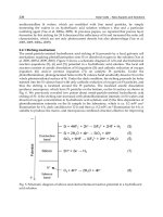
203
diode model (Fig. 1a) or to an equivalent circuit of two-diode model (Fig. 1b) containing
photocurrent source, a diode or two diodes, a shunt resistor and a series resistor in the load
branch.
(a) (b)
Fig. 1. The equivalent circuits of one-diode and two-diode models of a solar cell.
One-diode model and two-diode model can be represented by Eqs. (1) and (2) accordingly:
s
T
viR
V
s
ph 0 T
p
viR
nkT
iI I(e 1) , V
Rq
(1)
ss
T1 T2
viR viR
j
VV
s
ph 01 02 Tj
p
nkT
viR
iI I(e 1)I(e 1) , V
j
1,2
Rq
(2)
Where, one-diode model has five unknown parameters;
ph 0 s
I,I,n,R and
p
Rand the two-
diode model has seven unknown parameters;
ph 01 1 02 2 s
I,I,n,I,n,R and
p
R. On the other
hand, a solar panel is composed of parallel combination of several cell strings and a string
contains several cells in series. Therefore, the both models can be also stated for a solar
panel. In this research, the idea is to compare the accuracy of the two mentioned models for
a solar panel. As it is known, the unknown parameters of the models are functions of the
incident solar irradiation and panel temperature; hence dependency between them should
be taken into account.
In this section, evaluation of the unknown one-diode model parameters based on five
equations are presented. The specific five points (are shown in Fig. 2) on the I-V curve are
used to define the equations, where
sc
I is the short circuit current,
x
I is the current at
xoc
V0.5V ,
xx
I is current at
xx oc mp
V0.5(VV)
,
oc
V is the open circuit voltage and
mp
V
is the voltage at the maximum power point. In this study, the mentioned points are
generated for 113 operating conditions between 15-65°C and 100-1000W/m
2
to solve the five
coupled implicit nonlinear equations for a solar panel that consists of 36 series connected
poly-crystalline silicon solar cells at different operating conditions. By solving the nonlinear
equations in a specific environmental condition, we will find five unknown parameters of
the model in one operating condition. Equation (3) shows the system nonlinear equations
for one-diode model.
s
viR
s
a
jjph0
p
viR
nkT
FiII(e ) ,a
j
1,2, ,5
Rq
(3)
Rp
Diode
Rs
Iph
+
-
V
I
Rp
D1
Rs
Iph
+
-
V
I
D2
Solar Cells – Silicon Wafer-Based Technologies
204
Fig. 2. Five points on the I-V curve of a solar panel are used to solve the nonlinear equations.
Former approach is used to solve seven coupled implicit nonlinear equations of the two-
diode model for a solar panel. The specific seven points (are shown in Fig. 3) on the I-V
curve are used to define the equations, where
b
I
is the current at
mp
b
V
V
3
,
c
I
is the
current at
mp
c
2V
V
3
,
e
I
is the current at
mp oc
e
2V V
V
3
and
f
I
is the current at
mp oc
f
V2V
V
3
.
Fig. 3. Seven points on the I-V curve of a solar panel to solve the nonlinear equations.
Evaluation the Accuracy of One-Diode and Two-Diode
Models for a Solar Panel Based Open-Air Climate Measurements
205
The points are also generated for the 113 operating conditions to solve the seven coupled
implicit nonlinear equations for the solar panel. Solving the nonlinear equations in a specific
environmental condition leads to define seven unknown model parameters in one operating
condition. Equation (4) shows the system nonlinear equations for the two-diode model.
ss
12
viR viR
aa
s
jjph01 02
p
k
k
viR
GiII(e 1)I(e 1) ,
R
nkT
a , k 1,2 , j 1,2, ,7
q
(4)
Figs. 4 and 5 show the implemented algorithms in order to solve the nonlinear equations for
the both models.
3. Measurement system
A block diagram of a measurement system is shown in Fig. 6. The main function of this
system is extracting the solar panel’s I-V curves. In this system, an AVR microcontroller
(ATMEGA64) is used as the central processing unit. This unit measures, processes and
controls input data. Then the processed data transmit to a PC through a serial link. In the
proposed system, the PC has two main tasks; monitoring (acquiring the results) and
programming the microcontroller. Extracting the solar panel’s I-V curves shall be carried out
in different environmental conditions. Different levels of received solar irradiance are
achieved by changing in solar panel’s orientation which is performed by controlling two DC
motors in horizontal and vertical directions. Although the ambient temperature changing is
not controllable, the measurements are carried out in different days and different conditions
in order to cover this problem. A portable pyranometer and thermometer are used for
measuring the environmental conditions; irradiance and temperature. Hence, 113 acceptable
I-V curves
(out of two hundred) were extracted. Motor driver block diagram is also shown in
Fig. 7. Driving the motors is achieved through two full bridge PWM choppers with current
protection. Table 1 reports electrical specifications of the under investigation solar panel at
standard conditions based on datasheets.
Solar Panel Poly-Crystalline Silicon Solar Panel
Standard conditions
Irradiance (W/m
2
)
1000
Temperature (°C)
25
I
sc
(A) 2.98
V
oc
(V) 20.5
I
m
pp
(A) 2.73
V
m
pp
(V) 16.5
P
m
pp
(W) 45
n
s
36
n
p
1
k
i
(%/°C ) 0.07
k
v
(mv/°C) -0.038
Table 1. Datasheet information of the under investigation solar panel
Solar Cells – Silicon Wafer-Based Technologies
206
Fig. 4. Flowchart of extraction the one-diode model parameters
Evaluation the Accuracy of One-Diode and Two-Diode
Models for a Solar Panel Based Open-Air Climate Measurements
207
Fig. 5. Flowchart of extraction the two-diode model parameters
Solar Cells – Silicon Wafer-Based Technologies
208
Fig. 6. Block diagram of the proposed measurement system
Fig. 7. Motor driver block diagram
3.1 The I-V curve extractor
There is an important rule for solar panel’s I-V curves in photovoltaic system designing.
Although the manufacturers give specifications of their products (cell or panel) generally in
the standard condition, behavior of solar cells and panels are more required in non-standard
Control Unit &
Electronic Load
Programming
& Monitoring
Interface
Input
Power
Temperature
Sensor
Pyranometer
(Radiation)
Solar Panel
Amp Volt
Power Supply
M
Vertical Motor
M
Horizental Motor
Motors Driver
Control & PWM
signals for motors
Evaluation the Accuracy of One-Diode and Two-Diode
Models for a Solar Panel Based Open-Air Climate Measurements
209
environmental conditions. In order to extract a solar panels’ I-V curve, it is sufficient to
change the panel current between zero (open-circuit) to its maximum value (short-circuit)
continuously or step by step when environmental condition was stable (the incident solar
irradiance and panel temperature). Then the characteristic curve could be obtained by
measuring the corresponding voltages and currents. Therefore, a variable load is required
across the panel output ports.
Since the solar panel’s I-V curve is nonlinear, the load variation profile has a significant
impact on the precision of the extracted curve. If the load resistance (or conductance) varies
linearly, the density of the measured points will be high near I
sc
or V
oc
and it is not desired.
Hence, the nonlinear electronic load is more suitable. There are generally two methods for
implementation a variable load, which will be discussed below.
3.1.1 Discrete method
As mentioned above, extracting the solar panel I-V curve could be carried out by its output
load variation. An easy way is switching of some paralleled resistors to have different loads.
If the resistors have been chosen according to Eq. (5), it is possible to have 2
n
different load
values by switching of n resistors.
nn1
1
RR
2
(5)
The schematic for the proposed switching load is shown in Fig. 8. This method may cause
some switching noise in the measurement system. Therefore, a controllable continuous
electronic load is suitable.
Fig. 8. The proposed switching load circuit
3.1.2 Continuous method
The schematic diagram for the proposed continuous electronic load is shown in Fig. 9. The
drain-source resistor of a MOSFET in linear area of its electrical characteristic curves is used
as a load. As we know, the value of this resistor could be controlled by gate-source voltage.
Mathematical relationship between the value of this resistor and applied voltage is
described in Eq. (6).
ox
ds
g
sT
tL
1
R
WV V
(6)
Solar Cells – Silicon Wafer-Based Technologies
210
Fig. 9. The proposed continuous electronic load
In this equation,
L
is channel length, W is channel width,
is electric permittivity,
is
electron mobility and
ox
t
is oxide thickness in the MOSFET. Implementation of this method
is much quicker and easier than the previous one, and doesn’t induce any switching noise in
the measurement system. Simulation results and the measured data for the proposed
electronic load (continuous method) are performed by Orcad/Pspice 9.2. The simulation
result and experimental data are shown in Fig. 10. We observed that the simulation result
and experimental data have similar electrical behavior. Their difference between curves was
raised because of error in measurement and inequality real components with components in
the simulation program. Anyway, the proposed electronic load (continuous method) was
suitable for our purpose.
Fig. 10. Experimental data and simulation results of continuous electronic load profile
Evaluation the Accuracy of One-Diode and Two-Diode
Models for a Solar Panel Based Open-Air Climate Measurements
211
The schematic diagram of the implemented continuous electronic load is shown in Fig. 11.
Fig. 11. The schematic diagram of continuous electronic load
Fig. 12 shows a typical extracted I-V and P-V curves by this method in the following
conditions; irradiance = 500 w/m
2
and temperature = 34.5 °C. It is observed that the
proposed electronic load could be suitable to extract the solar panel’s I-V curves.
Fig. 12. A typical extracted solar panel’s I-V curve
4. The extracted models unknown parameters
The Newton method is chosen to solve the nonlinear equations. A modification is also
reported in the Newton's solving approach to attain the best convergence. MATLAB
software environment is used to implement the nonlinear equations and their solving
method. At first, the main electrical characteristics
sc oc mp mp
(I ,V ,V &I )are extracted for all I-
V curves of the solar panel (extracted by the measurement system) which Table 2 shows
them. The main electrical characteristics of the solar panel are used in nonlinear equations
models.
To PC
R310k
R4
.11
LOAD+
R7
4.7k
M2
IRF540
R2270k
C2
100n
R5
100
R1
10k
+5V
-VCC
U1A
LF353/NS
3
2
84
1
+
-
V+V-
OUT
0
D2
R6
1k
0
D3
From PC
VCC
0
-VCC
VCC
R8
1.6k
0
R10
1k
0
0
R11
47K
R9
1k
LOAD-
-
+
U2
AD620
2
6
74
81
3
5
Solar Cells – Silicon Wafer-Based Technologies
212
The I-V
Curves
Environmental Conditions
V
oc
(V)
I
sc
(A)
V
mp
(V)
I
mp
(A)
Irradiance
(W/m
2
)
Temperature
(°C)
1 644.30 22.95 20.58 1.90 15.55 1.67
2 657.70 24.00 20.53 1.94 15.52 1.70
3 662.18 24.50 20.50 1.95 15.55 1.70
4 665.16 25.20 20.50 1.97 15.60 1.71
5 668.85 25.20 20.50 1.98 15.40 1.74
6 456.36 15.20 21.10 1.35 16.43 1.21
7 467.55 14.50 21.15 1.39 16.50 1.22
8 478.00 14.15 21.15 1.43 16.50 1.24
9 558.50 17.80 21.00 1.63 16.14 1.47
10 529.50 17.90 20.90 1.57 16.17 1.38
11 575.00 17.40 20.90 1.70 16.10 1.49
12 601.00 18.10 20.90 1.77 16.00 1.55
13 605.50 18.45 20.90 1.78 16.10 1.56
14 474.25 13.65 21.00 1.38 16.40 1.22
15 495.15 14.20 21.00 1.45 16.30 1.27
16 528.00 18.30 20.60 1.53 16.00 1.34
17 528.00 18.45 20.60 1.54 15.95 1.36
18 537.00 18.30 20.58 1.56 15.86 1.37
19 557.80 21.00 20.28 1.61 15.35 1.44
20 548.80 22.00 20.25 1.59 15.47 1.40
21 524.25 21.5 20.22 1.51 15.50 1.36
22 517.50 20.65 20.19 1.47 15.47 1.31
23 533.15 19.85 20.45 1.53 15.92 1.39
24 946.25 40.85 18.95 2.65 13.00 2.29
25 945.50 42.90 18.93 2.64 12.91 2.30
26 778.50 33.40 20.30 2.26 14.60 1.97
27 762.30 33.15 20.22 2.22 14.70 1.94
28 789.00 34.15 20.22 2.28 14.48 2.03
29 782.25 33.80 20.27 2.27 14.60 2.01
30 391.20 41.80 18.34 1.43 13.67 1.26
31 914.95 21.95 20.50 2.56 14.76 2.21
32 917.95 23.85 20.30 2.58 14.42 2.25
33 923.20 27.00 20.00 2.60 14.15 2.25
34 1004.50 34.60 19.10 2.82 13.00 2.42
35 1004.50 35.15 19.07 2.83 12.91 2.43
36 994.75 34.25 19.04 2.80 13.08 2.39
37 900.80 34.90 18.98 2.62 13.05 2.26
38 899.30 35.55 18.98 2.63 13.33 2.22
39 808.30 36.40 18.84 2.45 13.16 2.11
40 811.30 36.80 18.84 2.47 13.08 2.13
41 630.90 36.10 18.73 2.13 13.36 1.85
Evaluation the Accuracy of One-Diode and Two-Diode
Models for a Solar Panel Based Open-Air Climate Measurements
213
The I-V
Curves
Environmental Conditions
V
oc
(V)
I
sc
(A)
V
mp
(V)
I
mp
(A)
Irradiance
(W/m
2
)
Temperature
(°C)
42 633.85 36.20 18.79 2.13 13.39 1.85
43 637.55 35.85 18.84 2.14 13.44 1.86
44 406.40 34.10 18.70 1.59 13.81 1.40
45 412.35 33.00 18.87 1.61 14.10 1.40
46 1006.70 33.05 19.46 2.82 13.30 2.43
47 1014.20 33.20 19.38 2.85 13.22 2.45
48 1014.90 33.95 19.32 2.86 13.19 2.45
49 599.50 44.10 17.86 2.00 12.54 1.73
50 756.85 50.55 17.92 2.23 12.63 1.86
51 776.20 50.35 17.97 2.29 12.37 1.94
52 759.90 50.10 18.06 2.32 12.54 1.93
53 769.55 49.55 18.11 2.33 12.71 1.96
54 590.60 48.20 18.00 1.93 12.94 1.64
55 392.25 45.35 17.94 1.45 13.28 1.27
56 701.00 36.40 19.13 2.17 13.75 1.88
57 822.55 36.55 19.21 2.41 13.53 2.09
58 815.00 36.25 19.21 2.39 13.44 2.07
59 937.35 35.90 19.35 2.61 13.36 2.27
60 948.10 35.40 19.43 2.61 13.73 2.24
61 458.65 37.40 19.60 1.72 14.60 1.52
62 455.65 37.60 19.58 1.72 14.43 1.53
63 602.50 38.40 19.63 1.99 14.34 1.75
64 706.90 38.45 19.66 2.17 14.20 1.90
65 705.40 36.60 19.69 2.16 14.32 1.89
66 703.90 38.70 19.66 2.16 14.37 1.87
67 780.75 37.00 19.86 2.27 14.43 1.96
68 777.75 36.40 19.91 2.25 14.32 1.98
69 777.00 35.80 19.97 2.24 14.57 1.95
70 886.60 44.45 19.38 2.52 13.84 2.14
71 879.15 44.25 19.41 2.43 13.75 2.12
72 830.70 40.05 19.58 2.41 14.03 2.10
73 818.80 40.30 19.60 2.40 14.06 2.07
74 749.45 38.95 19.66 2.26 14.12 1.99
75 746.45 38.70 19.69 2.26 14.23 1.98
76 604.75 45.95 17.75 2.00 12.49 1.73
77 987.30 48.80 17.89 2.71 11.93 2.3
78 981.05 50.00 17.83 2.68 12.09 2.23
79 519.00 33.70 19.29 1.79 14.09 1.59
80 516.00 34.90 19.24 1.79 14.29 1.56
81 615.95 36.35 19.10 2.00 13.95 1.74
82 615.20 36.50 19.07 2.00 13.81 1.74
Solar Cells – Silicon Wafer-Based Technologies
214
The I-V
Curves
Environmental Conditions
V
oc
(V)
I
sc
(A)
V
mp
(V)
I
mp
(A)
Irradiance
(W/m
2
)
Temperature
(°C)
83 648.75 37.90 19.38 2.08 14.23 1.79
84 778.50 35.70 19.80 2.37 14.46 2.02
85 836.70 25.00 20.78 2.4 15.16 2.12
86 850.10 25.40 20.78 2.45 15.24 2.13
87 839.65 23.15 20.90 2.43 15.22 2.14
88 838.16 23.05 20.90 2.42 15.22 2.14
89 844.15 23.35 20.90 2.43 15.22 2.14
90 781.50 20.80 21.07 2.24 15.55 2.00
91 775.50 20.45 21.07 2.23 15.75 1.96
92 612.25 15.55 21.43 1.78 16.54 1.57
93 609.25 15.00 21.46 1.77 16.48 1.57
94 601.75 14.75 21.46 1.75 16.68 1.55
95 240.85 31.40 18.59 1.08 14.46 0.93
96 241.60 31.65 18.48 1.08 14.26 0.94
97 876.20 35.40 19.13 2.42 13.53 2.08
98 873.25 36.45 19.13 2.40 13.56 2.06
99 453.40 34.10 18.90 1.64 14.03 1.44
100 617.40 38.50 19.60 2.00 14.54 1.74
101 620.40 37.40 19.60 2.00 14.43 1.75
102 453.40 37.00 19.35 1.64 14.63 1.48
103 678.60 14.75 21.54 1.91 16.26 1.70
104 718.10 13.15 21.71 2.05 16.43 1.83
105 615.20 33.10 19.77 2.09 14.48 1.79
106 589.10 33.55 19.72 1.95 14.63 1.70
107 649.50 37.85 19.35 2.09 13.92 1.83
108 648.05 37.90 18.79 2.08 13.42 1.82
109 653.95 38.15 18.76 2.08 13.33 1.83
110 665.20 39.20 18.73 2.13 13.19 1.87
111 947.05 42.55 18.90 2.65 13.02 2.28
112 454.90 37.75 18.73 1.64 13.84 1.44
113 458.65 36.10 18.68 1.64 13.92 1.42
Table 2. The main electrical characteristic of the panel
Then, the five and the seven nonlinear equations of the models are implemented and the
nonlinear least square approach is used to solve them. Tables 3 and 4 show the extracted
unknown parameters of the models for environmental conditions.
Irradiance
(W/m
2
)
Temperature
(°C)
I
ph
(A) I
0
(A) a Rs(Ω) Rp(Ω)
1 644.30 22.95 1.9054 1.3645×10
-7
1.2544 1.2078 279.6413
2 657.70 24.00 1.9406 2.0381×10
-7
1.2807 1.1805 287.2463
3 662.18 24.50 1.9579 1.0977×10
-7
1.2311 1.2276 252.0760
Evaluation the Accuracy of One-Diode and Two-Diode
Models for a Solar Panel Based Open-Air Climate Measurements
215
Irradiance
(W/m
2
)
Temperature
(°C)
I
ph
(A) I
0
(A) a Rs(Ω) Rp(Ω)
4 665.16 25.20 1.9738 9.0465×10
-8
1.2164 1.2520 255.1335
5 668.85 25.20 1.9776 1.4502×10
-7
1.2513 1.2238 253.4728
6 456.36 15.20 1.3443 2.0084×10
-7
1.3468 1.0289 475.3187
7 467.55 14.50 1.3822 5.7962×10
-8
1.2489 1.1676 303.7811
8 478.00 14.15 1.4235 5.2113×10
-8
1.2401 1.1492 228.1600
9 558.50 17.80 1.6448 1.6758×10
-7
1.3089 1.1391 488.4681
10 529.50 17.90 1.5640 1.3622×10
-7
1.2908 1.1252 305.8098
11 575.00 17.40 1.6993 1.4140×10
-7
1.2872 1.1635 280.1520
12 601.00 18.10 1.7753 1.0810×10
-7
1.2614 1.1667 252.2827
13 605.50 18.45 1.7854 1.8325×10
-7
1.3034 1.1494 313.9411
14 474.25 13.65 1.3814 2.0780×10
-7
1.3435 0.9994 307.3284
15 495.15 14.20 1.4413 2.1472×10
-7
1.3430 1.0062 275.3528
16 528.00 18.30 1.5321 2.1087×10
-7
1.3087 1.0844 307.3237
17 528.00 18.45 1.54442 1.8252×10
-7
1.2961 1.1175 303.6138
18 537.00 18.30 1.5615 9.6833×10
-8
1.2447 1.1485 245.5091
19 557.80 21.00 1.6145 3.2875×10
-7
1.3193 1.1212 354.5386
20 548.80 22.00 1.5919 2.1440×10
-7
1.2835 1.1649 305.2178
21 524.25 21.50 1.5309 5.5771×10
-7
1.3667 1.0884 474.5784
22 517.50 20.65 1.4714 3.9398×10
-7
1.3375 1.0842 405.6716
23 533.15 19.85 1.5753 2.1603×10
-7
1.2953 1.1464 805.5353
24 946.25 40.85 2.6666 8.9271×10
-7
1.2757 1.3558 146.2230
25 945.50 42.90 2.6574 1.2424×10
-6
1.3030 1.3219 150.3004
26 778.50 33.40 2.1973 3.1128×10
-7
1.2892 1.2567 515.2084
27 762.30 33.15 2.2171 5.3812×10
-7
1.3316 1.1894 210.1448
28 789.00 34.15 2.2886 3.9798×10
-7
1.3028 1.2315 214.3753
29 782.25 33.80 2.2765 5.0119×10
-7
1.3266 1.1978 212.4934
30 391.20 41.80 1.4409 2.2284×10
-6
1.3744 1.2030 357.0918
31 914.95 21.95 2.5657 2.9407×10
-7
1.2866 1.2771 178.6504
32 917.95 23.85 2.5853 4.0314×10
-7
1.2993 1.2704 179.9606
33 923.20 27.00 2.6220 5.5929×10
-7
1.3065 1.2800 142.9452
34 1004.50 34.60 2.8279 1.2215×10
-6
1.3071 1.3467 155.7048
35 1004.50 35.15 2.8362 1.5357×10
-6
1.3258 1.3260 151.6557
36 994.75 34.25 2.8140 1.2354×10
-6
1.3051 1.3258 141.9868
37 900.80 34.90 2.6385 2.1545×10
-6
1.3585 1.3032 170.0669
38 899.30 35.55 2.6449 1.5551×10
-6
1.3278 1.3082 152.1797
39 808.30 36.40 2.4663 1.5142×10
-6
1.3214 1.3244 186.9949
40 811.30 36.80 2.4866 8.9032×10
-7
1.2740 1.3574 152.6324
41 630.90 36.10 2.1335 7.5213×10
-7
1.2650 1.3213 179.3817
42 633.85 36.20 2.1493 1.4614×10
-6
1.3279 1.2659 172.9979
43 637.55 35.85 2.1526 1.3956×10
-6
1.3272 1.2720 181.0577
44 406.40 34.10 1.5971 1.7433×10
-6
1.3672 1.1656 253.3236
45 412.35 33.00 1.6220 1.0427×10
-6
1.3288 1.1815 221.4351