Solar Cells Silicon Wafer Based Technologies Part 14 potx
Bạn đang xem bản rút gọn của tài liệu. Xem và tải ngay bản đầy đủ của tài liệu tại đây (1.25 MB, 25 trang )
Solar Cells – Silicon Wafer-Based Technologies
316
We notice that after the irradiation of ITO/InP solar cells with an integral proton flux of
10
13
cm
-2
, their efficiency decreases by 26%, that is less than in the case of Si and GaAs based
solar cells. In the spectral characteristics of ITO/pInP solar cells after proton irradiation a
small decrease of the photosensitivity in the long wavelength region of the spectrum was
observed due to the decrease of the diffusion length.
Comparing the results of the radiation stability study of ITO/InP SC, fabricated by spray
pyrolysis, with the results of similar investigations of other InP based structures, it is
possible to conclude that in this case the radiation stability is also determined by the low
efficiency of radiation defects generation and, hence, by the low concentration of deep
recombination centers, reducing the efficiency of solar energy conversion in electric power.
3. Fabrication of ITO/nSi solar cells with enlarged area by spray pyrolisys
From the brief discussion above it can be concluded that the deposition of ITO layers by
spray pyrolysis on the surface of different semiconductor materials allows manufacturing
SC through a simple and less expensive technology. The most effective are ITO/InP SC but
because of a very high cost of the InP crystals they cannot be widely used in terrestrial
applications. To this effect ITO/nSi SC with the efficiency higher than 10% may be used, but
it is necessary to develop the technology for SC fabrication with the active area enlarged up
to 70-80 cm
2
as is the case of traditional silicon SC with p-n junction.
3.1 Deposition of ITO layers on enlarged silicon wafers
ITO layers are deposited on the nSi crystals surface using the specially designed installation
(Simashkevich et al., 2004; Simashkevich et al., 2005) (Fig. 15) that has four main units: the
spraying system (7), the system of displacement and rotation of the support on which the
substrate is fixed (4, 5), the system of heating the substrate, and the system of the evacuation of
the residual products of the pyrolysis (8). The heating system consists of an electric furnace (2)
and a device for automatic regulation of the substrate temperature with the thermocouple (3).
The rest of the installation parts are: the power unit (1), the cover (10), and the shielding plate
(12). Silicon wafers (11) are located on the support (9) and with the displacement mechanism
are moved into the deposition zone of the electric furnace (6). The construction of this
mechanism provides the rotation of the support with the velocity of 60 rotations per minute,
the speed necessary for the obtaining of thin films with uniform thickness on the all wafer
surface. The alcoholic solution of the mixture SnCl
4
+ InCl
3
is sprayed with compressed
oxygen into the stove on the silicon wafer substrate, where the ITO thin film is formed due to
thermal decomposition of the solution and the oxidation reaction. On the heated up substrate
there are the chemical reactions describe above in formulas (1) and (2).
The BSF n/n
+
junction was fabricated on the rear side of the wafer by a diffusion process
starting from POCl
3
gas mixture. The junction formation ended with a wet chemical etching
of POCl
3
residual in a 10% HF bath. A junction depth of 1μm was chosen in order to
minimize recombination. To reduce the surface recombination velocity the wafers were
thermally oxidized at the temperature of 850
o
C. The main steps of the fabrication of BSC are
schematized in Fig. 16.
3.2 Properties of ITO layers
The properties of the thus obtained ITO films depend on the concentration of indium
chloride and tin chloride in the solution, the temperature of the substrate, the time of
Solar Cells on the Base of Semiconductor-Insulator-Semiconductor Structures
317
spraying and the deposition speed. ITO films had a microcrystalline structure that was
influenced by the crystal lattice of the support as the X-ray analysis showed. They had cubic
structure with the lattice constant 10.14Å (Bruk et al., 2009)). The SEM image of such an ITO
film is presented in Fig. 17.
(a) (b)
Fig. 15. Schematic a) and real b) view of the installation for ITO thin films deposition
ITO/SiO
2
/nSi solar cells with the active area of 8.1cm
2
and 48.6cm
2
were fabricated. In some
cases a BSF region was obtained at the rear contact by phosphor diffusion.
Fig. 16. SC process sequence.
Solar Cells – Silicon Wafer-Based Technologies
318
Fig. 17. SEM image of ITO film
From Fig. 17 it is clear that the ITO film with the thickness of 400nm has a columnar
structure, the column height being about 300nm and the width 50-100nm.
ITO films with the maximum conductivity 4.7·10
3
Om
-1
cm
-1
, the electron concentration
(3.5÷15)·10
21
cm
-3
,
,
the mobility (15÷30)cm
2
/(V·s). and maximum transmission coefficient in
the visible range of the spectrum (87 %) were obtained from solutions containing 90 % InCl
3
and 10 % SnCl
4
at the substrate temperature 450°C, deposition rate 100 Å/min, spraying
time 45 s. ITO layers with the thickness 0.2mm to 0.7mm and uniform properties on the
surface up to 75cm
2
were obtained.
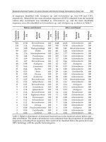
The dependence of the electrical parameters of ITO layers as a function of their composition
is given in Table 5.
Parameters
Ratio of InCl
3
:SnCl
4
:C
2
H
5
OH component in the solution
10:0:10 9.5:0.5:10 9:1:10 8.5:1.5:10 8:2:10 0:10:10
, S·cm
-1
2.6·10
2
2.6·10
3
4.7·10
3
2.6·10
3
1.3·10
3
42.4
n, cm
-3
1.1·10
20
5.5·10
20
1.1·10
21
6.5·10
20
5.8·10
20
5.3·10
19
μ, cm
-2
/(V·s) 15 29 27 25 14 5
Table 5. The dependence of the electrical parameters of ITO layers as a function of their
composition
The band gap width determined from the spectral dependence of the transmission
coefficient is equal to 3.90eV and changes only for the content of 90-100% of InCl
3
in the
spraying solution. If the content of InCl
3
is less than 90% the band gap remains constant and
equal to 3.44eV. The optical transmission and reflectance spectra of the deposited on the
glass substrate ITO thin films (Simashkevich et al., 2004) shows that the transparence in the
visible range of spectrum is about 80%, 20% of the incident radiation is reflected.
The ITO thin film thickness was varied by changing the quantity of the sprayed solution and
it was evaluated from the reflectance spectrum (Simashkevich et al., 2004). The thickness of
the layer was determined using the relationship (Moss et al., 1973):
d=λ
1
·λ
2
/{(λ
2
-λ
1
)·2n} (4)
where: n-refraction index equal to 1.8 for ITO (Chopra et al., 1983); λ-the wavelengths for
two neighboring maximum and minimum; d-the thickness of the ITO layer. Using this
relation the thickness of ITO layers deposited on the nSi wafer surface in dependence on the
quantity of the pulverized solution has been determined. This relation is linear and the layer
thickness varies from 0.35μm up to 0.5μm.
Solar Cells on the Base of Semiconductor-Insulator-Semiconductor Structures
319
3.3 Obtaining of ITO/nSi structures
The nSi wafers oriented in the (100) plane with resistivity 1.0 Ohm.cm and 4.5 Ohm.cm
(concentrations 5·10
15
cm
-3
and 1·10
15
cm
-3
) were used for the fabrication of SIS structures.
Insulator layers were obtained on the wafers surface by different methods: anodic, thermal
or chemical oxidation. The best results have been obtained at the utilization of the two last
methods. The chemical oxidation of the silicon surface was realized by immersing the silicon
wafer into the concentrated nitric acid for 15 seconds. A tunnel transparent for minority
carriers insulator layers at the ITO/Si interface have been obtained thermally, if the
deposition occurs in an oxygen containing atmosphere. Ellipsometrical measurement
showed that the thickness of the SiO
2
insulator layer varies from 30 Å to 60 Å. The frontal
grid was obtained by Cu vacuum evaporation. The investigation of the electrical properties
of the obtained SIS structures demonstrates that these insulator layers are tunnel transparent
for the current carriers. Thereby the obtained ITO/nSi SIS structures represent asymmetrical
doped barrier structures in which a wide band gap oxide semiconductor plays the role of
the transparent metal.
4. Physical properties of n
+
ITO/SiO
2
/nSi structures
4.1 Electric properties
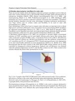
Current-voltage characteristics in the temperature range 293K–413K were studied. The general
behavior of the I-V curves of directly biased devices in Fig. 18 is characterized by the presence
of two straight-line regions with different slopes (Simashkevich et al., 2009). Two regions with
different behavior could be observed from this figure In the first region, at external voltages
lower than 0.3 V, the I-V curves are parallel, i.e., the angle of their inclination is constant.
0.00.10.20.30.40.50.60.7
10
-7
10
-6
10
-5
10
-4
10
-3
10
-2
10
-1
region 2
Different
slope
I (A)
U (V)
1-T= 20
o
C
2-T= 40
o
C
3-T= 60
o
C
4-T= 80
o
C
5-T=100
o
C
6-T=120
o
C
7-T=140
o
C
7
1
region 1
Equal
slope
Fig. 18. Temperature dependent direct I-V characteristics in the dark of the n
+
ITO/SiO
2
/nSi
solar cells
In this case, according to (Riben & Feucht, 1966), the charge carrier transport through
the potential barrier is implemented through the tunnel recombination processes in the
Solar Cells – Silicon Wafer-Based Technologies
320
space charge region, and the current-voltage dependence could be described by the
relation:
I = I
o
exp(AV) exp(BT) (5)
where A and B are constant and do not depend on voltage and temperature, respectively.
The numerical value of the constant A, determined from dependences presented in Fig. 18 is
equal to 15 V
-1
. The value of the constant B, which is equal to 0.045 K
-1
, was calculated from
the same dependences that have been re-plotted as lnI = f(T). In (Riben & Feucht, 1966) the
constant A is expressed by the relation:
A = 8π/3h·(m٭
e
ε
s
S/N
d
)
1/2
(6)
where m٭
e
– is the electron effective mass (in Si in the case considered); ε
s
– the dielectric
permeability of the silicon, and S represents the relative change of the electron energy after
each step of the tunneling process. Note that 1/S represents the number of tunneling steps.
(a) (b)
Fig. 19. The energy band diagram for: a) biases lower than 0.3 V (the region 1 in Fig. 18), b)
biases higher than 0.3 V (region 2 in Fig. 18)
The numerical value of A is easily calculated, since the other parameters in the respective
expression represent fundamental constants or Si physical parameters. Hence, the
mechanism of the charge carrier transport at direct biases of less than 0.3 V could be
interpreted as multi-step tunnel recombination transitions of electrons from the silicon
conduction band into the ITO conduction band (see the energy band diagram in Fig.19a), the
number of steps being about 100.
At voltages higher than 0.3 V (see different slope region in Fig. 18) the current flow
mechanism through the ITO/nSi structure changes. The slopes of the I-V curves become
temperature dependent that is confirmed by the constant value n about 1.6 of the parameter
n in the relation:
I = I
0
exp(qV
a
/nkT) (7)
where
I
0
= Cexp(-φ
B
/kT) (8)
C is a constant depending on the flux current model (emission or diffusion) (Milnes &
Feucht, 1972).
Solar Cells on the Base of Semiconductor-Insulator-Semiconductor Structures
321
Such an I-V dependence expressed by relations (7) and (8) is typical for transport
mechanisms involving emission of electrons over potential barriers (Fig. 19b). Thus, at
temperatures higher than 20°C, an initial voltage that stimulates the electron emission from
Si into ITO over the potential barrier at the Si/ITO interface in n
+
ITO/SiO
2
/nSi structures is
of about 0.3 V. From lnI = f (1/kT) it is possible to determine the height of the potential
barrier φ
B
in ITO/nSi structures because the slope of the above-mentioned dependence is
equal to φ
B
-qV
a
. The calculated value of φ
B
is 0.65eV, which is in correlation with the
experimental data. A close value of the height of the potential barrier φ
B
equal to 0.68 eV
was determined also from relation (8) (Simashkevich et al., 2009).
To sum up, in n
+
ITO/SiO
2
/nSi structures two mechanisms of the direct current flow are
observed: (i) tunneling recombination at direct voltages of less than 0.3 V and (ii) over
barrier emission at voltages higher than 0.3 V. In the former case, the direct current flow
could be interpreted as multi-step tunnel recombination transitions of electrons from the
silicon conduction band into the ITO conduction band, the number of steps being of about
100. The reduction of the influence of the former as well as a fine adjustment of the SiO
2
thickness in investigated structures will lead to an increased efficiency of converting solar
energy into electric energy.
4.2 Photoelectric properties
The spectral distribution of the quantum efficiency as well as the photosensitivity of the
obtained PV cells have been studied (Simashkevich et al., 2004). The monochromatic light
from the spectrograph is falling on a semitransparent mirror and is divided into two equal
fluxes. One flux fall on the surface of a calibrated solar cell for the determination of the
incident flux energy and the number (N) of incident photons. The second flux falls on the
surface of the analyzed sample and the short circuit current Jsc is measured, thus permitting
the calculation of the number of charge carriers, generated by the light and separated by the
junction, and then the quantum efficiency for each wavelength (Fig. 20).
400 600 800 1000 1200
0.0
0.1
0.2
0.3
0.4
0.5
0.6
0.7
0.8
0.9
1.0
0.0
0.1
0.2
0.3
0.4
0.5
0.6
0.7
0.8
0.9
1.0
Photo Sensitivity (A/W)
2
1
Quantum Efficiency
Wavelength (nm)
Fig. 20. Spectral distribution of the quantum efficiency (1) and photo sensitivity (2) of the
n
+
ITO/SiO
2
/nSi solar cells
Solar Cells – Silicon Wafer-Based Technologies
322
The reproducibility of the process and the performances of the devices during samples
realization were checked in each batch of samples as well as batch-to-batch. The
enlargement of the area of the solar cells up to 48.6cm
2
leads to the increasing of the series
resistance and to the diminishing of the efficiency down to 7%. Thus, the method of
obtaining n
+
ITO/SiO
2
/nSi structures based on the thin In
2
O
3
: Sn layers, which are formed
on the surface of Si wafers, traditionally chemically treated, passivated and heated to the
temperature of 450°C, by spraying chemical solutions of indium tin chloride was elaborated.
Solar cells based on n
+
ITO/SiO
2
/nSi structures with an active surface up to 48.6cm
2
have
been fabricated.
Maximum efficiency of 10.52% is obtained in the case of (100) crystallographic orientation of Si
wafer with BSF region at the rear surface and active area of 8.1 cm
2
, ITO thickness 0.3mm, SiO
2
thickness - 30Å and the concentration of charge carriers (electrons) in silicon (1-5)×10
15
cm
-3
(Fig. 21).
0.0 0.1 0.2 0.3 0.4 0.5
0
10
20
30
40
J
sc
= 36.3 mA/cm
2
V
oc
= 0.475 V
R
s
= 0.085 Ohm
Rsh = 6 Ohm
FF = 60.9 %
Eff.= 10.58 %
Standart conditions
1000W/m
2
, 25
o
C, AM1.5
Current density,mA/cm
2
Voltage,V
Fig. 21. Load I-V characteristic of the n
+
ITO–SiO
2
–nSi cells with active area 8.1cm
2
and BSF
region at rear surface.
The developed technology demonstrates the viability of manufacturing solar cells based on
n
+
ITO/SiO
2
/nSi junctions by assembling two 15W and two 30W power solar panels
(Fig. 22) (Usatii, 2011).
5. Bifacial n
+
Si/nSi/SiO
2
/n
+
ITO solar cells
For the first time BSC that are able to convert the solar radiation incident of both sides
of the cell into electric power have been produced and investigated fifty years ago (Mori,
1960). This type of SC has potential advantages over traditional monofacial SC. First, there
is the possibility of producing more electric power due to the absorption of solar energy
by the frontal and rear sides of the device, next, they do not have a continuous metallic
rear contact, therefore they are transparent to the infrared radiation, which warms
Solar Cells on the Base of Semiconductor-Insulator-Semiconductor Structures
323
the monofacial SC and reduces their efficiency. As was presented in (Cuevas, 2005),
different types of BSC have been fabricated since then, but all those BSC are based on
p-n junctions fabricated by impurity diffusion in the silicon wafer. In case of BSF
fabrication, these difficulties increase since it is necessary to realize the simultaneous
diffusion of different impurities, which have an adverse influence on the silicon
properties. Therefore, the problem of protecting the silicon surface from the undesirable
impurities appears.
(a) (b)
Fig. 22. General view of ITO/nSi photovoltaic converters a) SC with active aria 48.6 cm
2
, b)
solar modules with different power
A novel type of BSC formed only by isotype junctions was proposed in (Simashkevich et al.,
2007), where the possibility was demonstrated to build BSC on the base of nSi crystals and
indium tin oxide mixture (ITO) layers obtained by spraying that contain only homopolar
junctions with a n
+
/n/n
+
structure The utilization of such structures removes a considerable
part of the above-mentioned problems of BSC fabrication because a single diffusion process
is carried out.
5.1 Fabrication and characterization of n
+
ITO/SiO
2
/n/n
+
Si bifacial solar cells
In the work (Simashkevich et al., 2007) the results are presented of producing and
investigating the silicon based BSC only on majority carriers. The first frontal junction is a
SIS structure formed by an ITO layer deposited on the surface of n-type silicon crystal. The
starting material is an n-type doped (0.7–4.5Ohm·cm) single crystalline (100) oriented Cz-
Silicon 375μm thick nSi wafer with the diameter of 4 inches. The electron concentrations
were 10
15
cm
-3
- 10
17
cm
-3
.
An usual BSF structure consisting of a highly doped nSi layer obtained by phosphorus
diffusion was fabricated on the topside of the wafer by a diffusion process starting from
POCl
3
gas mixture. The rear n/n
+
junction formation ends with a wet chemical etching of
POCl
3
residual in a 10 % HF bath. A junction depth of 1 μm has been chosen in order to
minimize recombination.
To reduce the surface recombination velocity the wafers have been thermally oxidized at a
temperature of 850
o
C. Grids obtained by Cu evaporation in vacuum were deposited on the
Solar Cells – Silicon Wafer-Based Technologies
324
frontal and back surfaces for BSC fabrication. The schematic view of the bifacial ITO/nSi
solar cell is presented in Fig. 23.
(a) (b)
Fig. 23. The schematic a) and real b) view of the ITO/nSi BSC
The spectral distribution of the quantum efficiency of BSC, obtained on silicon wafers with
different electron concentration, has been studied at frontal and back illumination (Fig.24).
With the frontal illumination, in the region of the wavelengths from 400nm to 870nm the
value of QY changes in the limits 0.65–0.95. With the back illumination, QY is equal to 0.6–
0.8 in the same region of the spectrum (Bruk et al., 2009).
400 500 600 700 800 900 1000 1100 1200
0.0
0.1
0.2
0.3
0.4
0.5
0.6
0.7
0.8
0.9
1.0
QY, arb.un.
(nm)
1-(=1.0Ohm
cm)
2-(
=4.5Ohm
cm)
3-(
=4.5Ohm
cm)
4-(
=1.0Ohm
cm)
1
3
2
4
Fig. 24. Spectral distribution of the quantum efficiency 1, 2-frontal illumination; 3, 4-rear
illumination
Solar Cells on the Base of Semiconductor-Insulator-Semiconductor Structures
325
The I-V load characteristics at AM1.5 spectral distribution and 1000W/m
2
illumination are
presented in Fig.25.
0.00.10.20.30.4
0.000
0.005
0.010
0.015
0.020
0.025
0.030
0.035
Rear illum.
J
sc
= 13.23 mA/cm
2
V
oc
= 0.392 V
FF = 69.28 %
Eff.= 3.60%
Frontal illum.
J
sc
= 32.63 mA/cm
2
V
oc
= 0.425 V
FF = 68.29 %
Eff.= 9.47%
Current density, A/cm
2
Voltage, V
Fig. 25. The I-V load characteristics and the photoelectric parameters of the elaborated BSC
at AM1.5 spectral distribution and 1000W/m
2
illumination
The photoelectric parameters of the elaborated BSC have been determined in standard
AM1,5 conditions: for the frontal side V
oc
=0.425V, J
sc
=32.63mA/cm
2
, FF=68.29%, Eff.=9.47%,
R
ser
=2.08Ohm, R
sh
=6.7·10
3
Ohm; for the back side V
oc
=0.392V, J
sc
=13.23mA/cm
2
, FF=69.28%,
Eff.=3.6%, R
ser
=3.40Ohm, R
sh
=1.26·10
4
Ohm.
The summary efficiency of the BSC is equal to 13.07%.
5.2 n
+
ITO/SiO
2
/n/n
+
Si bifacial solar cells with textured surface of Si crystals
Using the method of n
+
ITO/SiO
2
/n/n
+
Si bifacial solar cells fabrication described in
(Simashkevich et al., 2007) with improved parameters in conformity with p.2 of this
communication, in (Simashkevich et al., 2011) two types of bifacial solar cells have been
obtained which have different profiles of silicon wafer surface (Fig. 26 and Fig. 27).
It is seen from these data that the effected technology optimization allows to increase of the
summary efficiency from 13.07% to 15.73% in the case of irregular etching of the silicon
surface and to 20.89% in the case of regular etching. The bifaciality ratio also increases from
0.38 up to 0.75.
On the basis of physical parameters of the silicon wafer, ITO layers and of the results of our
experiments, the energy band diagram of the n
+
Si/nSi/SiO
2
/n
+
ITO structure was proposed
(Simashkevich et al., 2007).
Solar Cells – Silicon Wafer-Based Technologies
326
0.0 0.1 0.2 0.3 0.4 0.5
0
5
10
15
20
25
30
35
Rear illumination
J
SC
= 22.5mA/cm
2
U
OC
= 0.461V
FF = 59.4%
Eff. = 6.20%
Frontal illumination
J
SC
= 34.6mA/cm
2
U
OC
= 0.478V
FF = 57.4%
Eff.= 9.53%
Current density, mA/cm
2
Voltage, V
Fig. 26. Load I-V characteristic of n
+
ITO/SiO
2
/n/n
+
Si BSC with irregular Si surface
0.0 0.1 0.2 0.3 0.4 0.5
0
5
10
15
20
25
30
35
Rear illumination
J
SC
= 25.6mA/cm
2
U
OC
= 0.458V
FF = 76.9%
Eff.= 8.98%
Frontal illumination
J
SC
= 34.3mA/cm
2
U
OC
= 0.461V
FF = 75.0%
Eff.= 11.91%
Voltage, V
Current density, mA/cm
2
Fig. 27. Load I-V characteristic of n
+
ITO/SiO
2
/n/n
+
Si BSC with regular Si surface
Solar Cells on the Base of Semiconductor-Insulator-Semiconductor Structures
327
Fig. 28. Energy band diagram of the bifacial Cu/n
+
ITO/SiO
2
/nSi/n
+
Si/Cu structure
Fig. 28 shows this energy band diagram at illumination in the short-circuit regime. At the
illumination through the frontal contact, the solar radiation is absorbed in the silicon wafer.
The light generated carriers are separated by the nSi/SiO
2
/ITO junction. The BSF of the
n
+
Si/nSi junction facilitate the transport of the carriers to the back contact. The same
processes take place at the illumination through the rear contact.
6. Conclusion
SC fabricated on the basis of semiconductor-insulator- semiconductor structures, obtained
by deposition of TCO films on the surface of different semiconductor solar materials (Si, InP,
CdTe etc) are promising devices for solar energy conversion due to the simplicity of their
fabrication and relatively low cost. One of the main advantages of SIS based SC is the
elimination of the high temperature diffusion process from the technological chain, which is
necessary for obtaining p-n junctions, the maximum temperature at the SIS structure
fabrication being not higher than 450
o
C. The TCO films can be deposited by a variety of
techniques among which the spray deposition method is particularly attractive since it is
simple, relatively fast and vacuum less. Between different TCO materials, the ITO layers are
the most suitable for the fabrication of SIS structures based solar cells.
Silicon remains the most utilized absorbing semiconductor material for fabrication by spray
pyrolysis of such type of SC. The maximum efficiency of ITO/nSi SC is 10-12%, but in the
case of textured surface of Si crystals the efficiency reaches more than 15%. ITO/nSi SC with
enlarged area up to 48 cm
2
have been obtained by the spray method, the efficiency is 10.58%
for cells with area of 8.1cm
2
.
Solar Cells – Silicon Wafer-Based Technologies
328
InP based SIS structures fabricated by deposition of ITO layers onto pInP crystal surfaces
have high efficiencies, at the same time they are more simple to fabricate in comparison with
diffusion junction cells. The efficiency of ITO/InP solar cells obtained by spray pyrolisis
depends on the crystallographic orientation of the InP wafers, The maximum efficiency of
11.6% was obtained in the case of fabrication of ITO/pInP/p
+
InP structures using InP
wafers oriented in the (110) plane. ITO/InP SC, obtained by spray pyrolysis demonstrates
radiation stability. After the irradiation of ITO/InP solar cells with an integral proton flux of
10
13
cm
-2
, their efficiency decreases by 26%, that is less than in the case of Si and GaAs based
solar cells.
A new type of bifacial solar cells n
+
Si/nSi/SiO
2
/n
+
ITO based only on isotype junctions was
elaborated and fabricated. It was demonstrated that the simultaneous illumination of both
frontal and rear surfaces of the structures allow to obtain a summary current. The
technological process of manufacturing such solar cells does not require sophisticated
equipment. Bifacial solar cells with summary efficiency of 21% and 65% bifaciality
coefficient have been obtained using as an absorbent material of single crystalline silicon
with a textured surface.
7. Acknowledgment
The authors would like to acknowledge Drs E.Bobeico and V.Fedorov for carrying out the
measurements of some parameters of ITO/nSi based solar cells, Dr. Iu.Usatii for the help in
developing the large-area deposition of ITO layers.
We thank the direction of the Institute of Applied Physics of the Academy of Sciences of
Moldova for support and creation of favorable conditions for investigations. We thank Dr.
Olga Iliasenco for technical assistance.
We also are grateful to those numerous scientists and engineers worldwide whose data have
been included in this overview.
8. References
Adeeb, N.; Kretsu, I.; Sherban, D.; Sushkevich, C. & Simashkevich, A. (1987). Spray
deposited ITO/CdTe solar cells. Solar Energy Materials, Vol. 15, No.1, (January 1987)
pp.9-19, ISSN 0927-0248
Aharoni, H.; Coutts, T.J.; Gessert, T.; Dhere, R. & Schilling L. (1986). Ion Beam Sputtered
Indium Tin Oxide for InP Solar Cells. Journal of Vacuum Science and Technology A,
Vacuum,Surfaces and Films. Vol. 4, No.3, pp. 428-431.
Aharoni, H. (1999). ITO/InP Photovoltaic Devices, Proc. of the International Solar Energy
Society (ISES) Solar World Congress, ISES 1999, SWC Israel. ISBN 008 043 8954, Vol. 1,
pp. 95-108, Jerusalem, Israel, (July 1999)
Anderson, R.L. (1975). Photocurrent suppression in heterojunctions solar cells.
Appl.Phys.Lett. Vol.27, No.12, (December 1975), pp.691-694, ISSN 0003-6951
Andronic, I.; Gagara, L.; Gorceak, L.; Potlog, T.; Sherban, D. & Simashkevich, A. (1998), InP
based radiation stable solar cells, Proc of the 2
nd
World Conf. on PV Solar Energy
Conversion, Vol.3, pp.3642-3645, ISBN 92-828-5179-6, Vienna, (July 1998)
Solar Cells on the Base of Semiconductor-Insulator-Semiconductor Structures
329
Ashok, S.; Sharma, P.P. & Fonash, S.J. (1980). Spray-deposited ITO–Silicon SIS heterojuction
solar cells. Electron Devices, IEEE Transactions on, Vol.27, No.4, 725-730, ISSN 0018-
9383
Bobeica, E.; Varsano, F.; Roca, F. & Parretta, A. (2001). Light backscattering properties of
textured silicon matirials, Book of abstracts. INFMMeeting – National Conferense on the
Physics of Matter, pp.242-243, Rome, Italy, (June 2001)
Botnariuc, V.M.; Gagara, L.S.; Gorchac, L.V.; Russu, E.V.; Simashkevich, A.V.; Sherban, D.A.
& Do Quoc Hung. (1990). ITO/InP surface barrier solar cells obtained by spray
method. Appl.Sol.Energy, No.3, pp.37-40, ISSN 0003-701X
Bruk, L.; Simashkevich, A.; Sherban, D.; Gorceac, L.; Coval, A. & Usatii, Iu. (2007). The
influence of thermal treatment on the parameters of nITO/pInP solar cells obtained
by pyrolithic spraying method, Proc. of the 22
th
European PV Solar Energy Conf.,
pp.672-674, ISBN: 3-936338-22-1, Milan, Italy, (September 2007)
Bruk, L.; Fedorov, V.; Sherban, D.; Simashkevicha, A.; Usatii, I.; Bobeico, E. & Morvillo P.
(2009). Isotype bifacial silicon solar cells obtained by ITO spray pyrolysis.
Materials Science and Engineering B, Vol.159–160, (March 2009), pp.282–285, ISSN
0921-5107
Calderer, J.; Manifacier, J.C.; Szepessy, L.; Darolles, J.M. & M. Perotin. (1979). Caractérisation
des cellules solaires silicium (n)-In2O3 (dope Sn) préparées par une méthode de
vaporisation. Revue de Physique Appliquée. Vol.14, No.3, page 485-490, HAL: jpa-
00244619, version 1
Chang, N.S. & Sites, R. (1978). Electronic characterization of indium tin oxide/silicon
photodiodes. J.Appl.Phys, Vol.49, No.9, (September 1978), pp.4833 -4837, ISSN 0021-
8979
Chapin, D.M.; Fuller, C.S. & Pearson, G.I. (1954). A New Silicon p-n Junction Photocell for
Converting Solar Radiation into Electrical Power, J. Appl. Phys., Vol. 25, No.5, (May
1954), pp.676-677, ISSN 0021-8979
Chopra, K.L.; Major S. & Pandya D.K. (1983). Transparent conductors. A status review. Thin
Solid Films, Vol.102, No.1, (April 1983), pp.1-46, ISSN 0040-6090
Cuevas, A. (2005). The early history of bifacial solar cells, Proc. of the 20
th
European
Photovoltaic Solar Energy Conference, pp.801-805, ISBN 3-936338-19-1, Barcelona,
Spain, (June 2005)
Dikusar, A.I.; Bruk, L.I.; Monaico, E.V.; Sherban, D.A.; Simashkevich, A.V. & Tiginyanu,
I.M. (2008). Photoelectric structures based on nanoporous p-InP. Surface
Engineering and Applied Electrochemistry, Vol.44, No.1, (February 2008), pp.1-5,
ISSN 1068-3755
DuBow, J.; Burk, D. & Sites, J. (1976). Efficient photovoltaic heterojunctions of indium tin
oxides on silicon. Appl.Phys.Lett., Vol.29, No.8, (October 1976), pp.494-496, ISSN
0003-6951
Feng, T.; Ghosh A.K. & Fishman C. (1979). Efficient electron-beam deposited ITO/nSi solar
cells. J.Appl. Phys., Vol.50, No.7, (June 1979), pp.4972-4974, ISSN 0021-8979
Gagara, L.; Gorcheac, L.; Radu, C.; Radu S.; Sherban, D. & Simaschkevici, A. (1996).
Photovoltaic converters of Solar Energy on the base of SIS structures, Proc. of the Int.
Conf. “Euro Sun 96”, Vol.2, pp.665-669, Munchen, (August 1996)
Solar Cells – Silicon Wafer-Based Technologies
330
Garcia, F.J.; Muci, J. & Tomar M.S. (1982). Preparation of (thin film SnO
2
)/(textured n-Si)
solar cells by spray pyrolysis. Thin Solid Films, Vol.97, No.1 (November 1982),
pp.47-51, ISSN 0040-6090
Gessert, T.A.; Li, X.; Wanlass, M.W. & Coutts, T.J. (1990). Progress in the ITO/InP Solar Cell,
Proc. of the second Int. Conf. ”Indium Phosphide and related materials”, pp.260-264,
Denver, CO, USA, (April 1990)
Gessert, T.A.; Li, X.; Coutts, T.J.; Phelps, P. & Tsafaras, W.N. (1991). Small-scale production
of 4cm
2
ITO/InP photovoltaic solar cells, Proc. of the third Int. Conf.” Indium
Phosphide and related materials”, pp.32-35, ISBN 0-87942-626-8, Cardiff, UK, (April
1991)
Horvath, Zs.J.; Subrahmanyam, A.; Manivannan, P. & Blasubramanian N. (1998). Electrical
and photovoltaic study of ITO/GaAs and ITO/InP heterojunctions, Proc of the 2
nd
World Conf. on PV Solar Energy Conversion, Vol.3, pp.3711-3714, ISBN 92-828-5179-6,
Vienna, (July 1998)
Jenkins, P.; Landis, G.A.; Fatemi, N.; Li,X.; Scheiman, D. & Bailey, S. (1992). Increased
efficiency with surface texturing in ITO/InP solar cells, Proc. of the fourth Int. Conf.
“Indium Phosphide and related materials”, pp.186-189, ISBN 0-87942-626-8, Newport,,
RI, USA, (April 1992)
Kobayashi, H.; Ishida,T.; Nakato, Y. & Tsubomura, H. (1991). Mechanism of carrier transport
in highly efficient solar sells having indium tin oxide/Si junction. J.Appl.Phys.
Vol.69, No.3, (February 1991), pp.1736-1743, ISSN 0021-8979
Li, X.; Wanlass M.W.; Gessert T.A.; Emery, K.A. & Coutts, T.J. (1989). High-efficiency
indium tin oxide/indium phosphide solar cells. Appl. Phys. Lett., Vol.54, No.26,
(June 1989), pp.2674-2676, ISSN 0003-6951
Malik, A.; Baranyuk, V. & Manasson, V. (1979). Solar cells based on the SnO
2
-SiO
2
-Si
heterojunction. Appl.Sol.Energy, No.2, pp.83-84, ISSN 0003-701X
Malik, A.; Baranyuk, V. & Manasson, V. (1980). Improved model of solar cells based on the
In
2
O
3
/SnO
2
/SiO
2
/nSi structure. Appl. Sol. Energy, No.1, pp.1-2, ISSN 0003-701X
Malik, O.; De la Hidalga-W, F.J.; Zuniga –I, C. & Ruiz-T, G. (2008). Efficient ITO/Si
solar cells fabricatd with a low temperature technology. Results and
perspectives. Journal of Non -Crystalline Solids, Vol.354, No.19-25, pp.2472-2477,
ISSN 0022-3093
Malik, O. & F.Javier De La Hidalga-W. (2009). Efficient Silicon Solar Cells Fabricated with a
Low Cost Spray Technique. In: Solar Energy, Radu D. Rugescu, pp. (81-104), In theh,
ISBN 978-953-307-052-0, Vukovar, Croatia
Manifacier, J.C. & Szepessy, L. (1977). Efficient sprayed In
2
O
3
:Sn n-type silicon
heterojunction solar cell. Appl. Phys. Lett., Vol.31, No.7, (October 1977), pp.459-462,
ISSN 0003-6951
Marques, F. & Chambouleyron, I. (1986). Surface barrier SnO
2
/SiO
x
/cSi(n) solar cells:
optimization of the fabrication process. Solar Cells, Vol.17, No.2-3 (April-May 1986),
pp.167-181, ISSN 0927-0248
Milnes, A.G. & Feucht, D.L. (1972). Heterojunctions and metal-semiconductor junctions,
Academic Press Inc (October 1972), ISBN-10 0124980503, ISBN-13 978-0124980501,
New-York and London, 408 p.
Solar Cells on the Base of Semiconductor-Insulator-Semiconductor Structures
331
Mizrah, T. & Adler, D. (1976). Operation of ITO-Si heterojunction solar cells. Appl.Phys.Lett.,
Vol.29, No.8, (November 1976), pp.682-684, ISSN 0003-6951
Moss, T.S.; Burrell, G.J. & Ellis B. (1973). Semiconductor Opto-Electronics, Butterworths,
London
Nagatomo, T.; Endo, M. & Omoto, O. (1979). Fabrication and characterization of SnO
2
/n-
Si solar cells. Jpn. J. Appl. Phys., Vol.18, No.6, (June 1979) pp.1103-1109, ISSN 0021-
4922
Nagatomo, T.; Inagaki, Y.; Amano, Y. & Omoto, O. (1982). A comparison of spray deposited
ITO/n-Si and SnO
2
/n-Si solar cells. Jpn. J. Appl. Phys., Vol.21, Suppl.21-2, pp.121-
124, ISSN 0021-4922
Riben, A.R. & Feucht, D.L. (1966). Electrical transport in nGe-pGaAs heterojunctions.
International Journal of Electronics, Vol.20, No.6, (June 1966), pp.583-599, ISSN 0020-
7217
Saim H.B. & Campbell D.S. (1987). Properties of indium-tin-oxide (ITO)/silicon
heterojunction solar cells by thick-film techniques. Solar Energy Materials, Vol.15
No.4, (May-June 1987), pp. 249-260, ISSN 0927-0248
Shewchun, J.; Dubow, G.; Myszhkowsky, A. & Singh, R. (1978). The operation of
semiconductor-insulator-semiconductor (SIS) solar cells: Theory. J. Appl. Phys.,
Vol.49, No.2, (February 1978), pp.855-864, ISSN 0022-3727
Shewchun, J.; Burk, D.; Singh, R.; Spitzer, M. & Dubow, G. (1979). The semiconductor-
insulator-semiconductor (indium tin oxide on silicon) solar cells: characteristics and
loss mechanisms. J.Appl.Phys. Vol.50, No.10, (October 1979), pp.6524-6533, ISSN
0021-8979
Shewchun, J.; Dubow, G.; Wilmsen, C.; Singh, R.; Burk, D. & Wagner J. (1979). The
operation of semiconductor-insulator-semiconductor (SIS) solar cells:
Experiment. J.Appl.Phys., Vol.50, No.4, (April 1979), pp.2832-2839, ISSN 0021-
8979
Shewchun, J.; Burc, D. & Spitzer, M.B. (1980). MIS and SIS solar cells. Electron Devices, IEEE
Transactions on. Vol.27, No.4, pp.705-716, ISSN 0018-9383
Simashkevich, A.; Toyi, J-M.; Sherban, D. & Yakubu, H. (1992). Investigation of ITO-GaAs
structures. Bull. of ASM, Phys.& Tech., No.3, pp.26-29
Simashkevich, A.; Do Quoc Hung; Bobeico, E.; Gorcheac, L. & Sherban, D. (1999). Solar cells
based on SIS structures, Proc. of the 3
rd
Int. Workshop on Material Science, Part.1,
pp.56-59, ISBN 90-5776-033-9, Hanoi, Vietnam, (November 1999)
Simashkevich, A.; Sherban, D.; Bruc, L.; Coval, A.; Fedorov, V.; Bobeico, E. & Usatii., Iu.
(2004). I. Spray-deposited ITO/nSi solar cells with enlarged area. Moldavian
Journal of Physical Sciences, Vol.3, No.3-4, (December 2004), pp.334-339, ISSN 1810-
648X
Simashkevich, A.; Serban, D.; Bruc, L.; Coval, A.; Fedorov, V.; Bobeico, E. & Usatii. Iu.
(2005). Spray deposited ITO/nSi solar cells with enlarged area, Proc. of the 20
th
European Photovoltaic Solar Energy Conference, pp.980-982, ISBN 3-936338-19-1,
Barcelona, Spain, (June 2005)
Solar Cells – Silicon Wafer-Based Technologies
332
Simashkevich, A.; Sherban, D.; Morvillo, P.; Bobeico, E.; Bruk, L. & Usatii, Iu. (2007). Bifacial
solar cells based on isotype junctions, Proc. of the 22
th
European PV Solar Energy
Conf., ISBN: 3-936338-22-1, Milan, Italy, (September 2007), pp.484-486
Simashkevich, A.; Sherban, D.; Rusu, M.; Bruk, L. & Usatii. Iu. (2009). ITO/nSi solar cells:
voltage dependent charge transport mechanisms, Proc. of the 24
th
European
Photovoltaic Solar Energy Conference, pp.2230-2232, ISBN: 3-936338-24-1, Hamburg,
Germany, (September 2009)
Simashkevich, A.; Serban, D.; Bruc, L.; Fyodorov, V.; Coval, A. & Usatii. Iu. (2010). Features
of the mechanism of a current flowing through an ITO/nSi isotype structure.
Surface engineering and applied electrochemistry, Vol.46, No.1, (February 2010), pp.40-
42, ISSN 1068-3755
Simashkevich, A.V.; Sherban, D.A.; Bruk, L.I.; Usatii, Iu.V. & Fedorov V.M. (2010).
Transparent Conductive Oxide Layers and Their Application in Solar Energetic.
Physics and Chemistry of Solid State, Vol.11, No.4, (October 2010), pp. 950-956
Simashkevich, A.V.; Sherban, D.A.; Bruk, L.I., Harea, E.E. & Usatii, Iu. (2011). Efficient
ITO/nSi solar cells with silicon textured surface. Elektronnaya Obrabotka Materialov,
Vol.47, No.3, ( May-June 2011), pp.79-84, ISSN 0013-5739
Tarr, N. & Pulfrey, D. (1979). New experimental evidence for minority-carrier. Appl. Phys.
Lett., V.34, No.4, (February 1979), pp.295-297, ISSN 0003-6951
Untila, G.G.; Chebotareva, A.V.; Osipov, A.S. & Samborsky, D.V. (1998). Series resistance of
solar cell with antireflection coating of transparent conducting oxide, Proc of the 2
nd
World Conf. on PV Solar Energy Conversion, Vol.1, pp.300-302, ISBN 92-828-5179-6,
Vienna, (July 1998)
Usatii, Iu. (2011). Preparation of ITO-Si solar cells with enlarged area and the study of their
properties. (in Romanian). Ph.D. Thesis, Chisinau, (February 2011)
Vasu, V. & Aubrahmanyam. A. (1992) Photovoltaic properties of indium tin oxide
(ITO)/silicon junctions prepared by spray pyrolysis - dependence on oxidation
time. Semicond. Sci. and Tech., Vol.7, No.3, (March 1992), pp.320-323, ISSN 0268-
1242
Vasu, V.; Subrahmanyam, A.; Kumar, J. & Ramasamy, P. (1993). Spray-pyrolytic-grown
ITO/InP junctions: effect of tin doping. Semicond. Sci. Technol., Vol.8, No.3 (March
1993) pp.437-440, ISSN 0268-1242
Wishwakarma, S., Rahmatullah R. & Prasad, H.C. (1993). Low cost SnO
2
:P/SiO
2
/n-Si
(textured) heterojunction solar cells. J.Phys.D:Appl.Phys., v.26, No.6, (June 1993),
pp.959-962, ISSN 0022-3727
Yamamoto, A.; Yamaguchi, M. & Uemura. C. (1984). High conversion efficiency and high
radiation resistance InP homojunction solar cells. Appl. Phys. Lett., Vol.44, No.6,
(March 1984), pp.611-614, ISSN 0003-6951
Michael Y. Levy
Hartsdale, New York
U.S.A.
1. Introduction
In this chapter, the author explains the present technological and scientific maturity of the
field of solar-energy conversion. The author builds on scientific foundations to generalize
several upper limits of solar-energy conversion as a function of the geometric-concentration
factor. These limits are used to define a high-efficiency regime for the terrestrial conversion
of solar-energy. The current world-record efficiency is measured in solar cells composed
of three junctions operating in tandem under a geometric-concentration factor of 454 Suns.
By illustrating that the current world-record efficiency is clearly within the high-efficiency
regime, the author argues that the field of photovoltaic solar-energy conversion is far removed
from its infancy. Inasmuch that the world-record efficiency is less than half of the theoretical
terrestrial limit, the author argues that there is significant space for scientific innovation.
In addition, by noting that the world-record efficiency, which is measured with a tandem
solar cell with three junctions operating at 454 Suns, is 9% less than the physical limit of a
tandem solar cells with two junctions operating under the same number of Suns, the author
makes apparent the potential for improvement to the present technological paradigm. The
author concludes that solar-energy science and technology has significantly more challenges
to address and innovations to realize before it may be considered a fully mature field.
The remainder of this chapter is organized as follows. In Section 2, the author describes
an ideal p-n junction solar cell and distinguishes the solar cell’s absorber, its function,
and its relation to the other essential components of the solar cell. In Section 3, the
author reviews three important approaches that establish upper-limiting efficiencies of
solar-energy conversion: the radiation-in-radiation-out approach of Landsberg and Tonge, the
omni-colour approach of DeVos, Grosjean, and Pauwels, and the detailed-balance approach
of Shockley and Queisser. The detailed-balance approach establishes the maximum-power
conversion-efficiency of a single p-n junction solar cell in the terrestrial environment as
40.7%. Yet, the omni-colour approach establishes the maximum-power conversion-efficiency
of solar energy in the terrestrial environment as 86.8%. In Section 4, the author reviews four
approaches for realizing a global efficiency enhancement with respect to the maximum-power
conversion-efficiency of a single p-n junction solar cell. The current technological paradigm
experimentally demonstrates high-efficiencies by using stacks of p-n junction solar cells
operating in tandem. Other next-generation approaches propose the incorporation of one or
more physical phenomena (e.g., multiple transitions, multiple electron-hole pair generation,
and hot carriers) to reach high-efficiencies. In Section 5, the author offers concluding remarks.
Maturity of Photovoltaic Solar-
Energy Conversion
15
2 Will-be-set-by-IN-TECH
2. Ideal p-n junction solar cell
In Figure 1, the present author illustrates the ideal electronic structure of a photovoltaic solar
cell (Würfel, 2002; Würfel, 2004), a device that converts the energy of radiation into electrical
energy. The ideal structure of the solar cell is comprised of several components: an absorber,
two emitters and two contacts. The absorber enables photo-chemical conversion, the emitters
enable electro-chemical conversion, and the contacts enable useful work to be performed by
an external load. In the following paragraphs, the present author describes an ideal solar cell
in more detail.
valence band
conduction band
ε
F,C
absorber
n-type
emitter
p-type
emitter
qV
Ohmic
contact
Ohmic
contact
h
ω
-
+
ε
F,V
μ
e-h
+
-
Fig. 1. Ideal structure of a solar cell. Shown is the absorber, which is sandwiched between an
n-type emitter and a p-type emitter. An Ohmic contact is made to each of the emitters. A
voltage, V, exists between the contacts of the solar cell.
An absorber is in the center of the solar cell. The absorber is a medium whose electronic
states form a conduction band and a valence band. The conduction and valence bands are
separated by an energetic gap that is characterized by the absence of electronic states. The
occupancy of the electronic states of the conduction band and valence band are described by
the quasi-Fermi energies ε
F,C
and ε
F,V
, respectively. The absorber is the region of the solar
cell where the absorption of photons occurs and where the subsequent photogeneration of
electrons and holes takes place. Ideally, each photon with energy greater than that of the
energetic gap may generate a single electron-hole pair. In such case, the energy of each photon
with energy greater than the bandgap is converted to the chemical energy of an electron-hole
pair, μ
e-h
,whereμ
e-h
= ε
F,C
− ε
F,V
(Würfel, 2002; Würfel, 2004).
The absorber is sandwiched between two semi-permeable emitters (Würfel, 2002; Würfel,
2004). The emitters are selected to produce an asymmetry in the band structure. The
electronegativity and bandgap of the emitter on the right (i.e., the n-type emitter) are selected
so that the (i) electrons largely or completely permeate through and (ii) holes largely or
completely do not (Würfel, 2002; Würfel, 2004). A small gradient drives the majority carriers
(i.e., holes) to the right so that a beneficial current is produced. A large gradient drives
minority carriers (i.e., electrons) to the right so that a detrimental current is produced. The
latter current is very small, resulting from the relative impermeability of the rightmost emitter
to electrons. The emitter on the left is similarly selected, except that it is the holes that
permeate through and yield a beneficial current.
334
Solar Cells – Silicon Wafer-Based Technologies
Maturity of Photovoltaic Solar-Energy Conversion 3
On the external surface of both emitters is a metallic contact. The carriers in the contacts are in
equilibrium with one another, so where the contact interfaces with the emitter the occupancy
of holes and electrons are described by the same Fermi energy. The absolute value of the
Fermi energy at the contact of the n-type emitter is roughly equal to the absolute value of the
quasi-Fermi energy of majority carriers at the interface between the absorber interfaces with
the n-type emitter. An analog of this statement holds for the contact to the p-type emitter.
Thus, between the two contacts there is a voltage, V, that is proportional to the potential
difference ε
F,C
− ε
F,V
as V =
(
ε
F,C
− ε
F,V
)
/q,whereq is the elementary charge. Therefore,
the chemical energy of each electron-hole pair, μ
e-h
, is converted to electrical energy by a unit
pulseofchargecurrent,q, at the voltage V. In the following subsection, the present author
reviews various limits describing the efficiency of solar-energy conversion.
3. Limits to ideal solar-energy conversion
In this section, the present author reviews three distinct approaches to upper-bound the
efficiency of solar-energy conversion. In Section 3.1, the present author offers a schematic
of a generalized converter and uses the schematic to define the conversion efficiency.
In sections 3.2, 3.3, and 3.4, the present author reviews the Landsberg-Tonge limit, the
Shockley-Queisser limit, and the omni-colour limit, respectively. In Section 3.5, the present
author compares and contrasts these three approaches. Finally, in Section 3.6, the present
author draws conclusions regarding the upper-theoretical efficiency of converting solar
energy to electricity in the terrestrial environment. The present author concludes that
though the efficiency limit of a single p-n junction solar cell is large, a significant efficiency
enhancement is possible. This is because, in the first approximation, the terrestrial limits of a
single p-n junction solar cell are 40.7% and 24.0%, whereas those of an omni-colour converter
are 86.8% and 52.9% for fully-concentrated and non-concentrated sunlight, respectively.
3.1 Generalized energy con verter
Figure 2 is a schematic of a generalized energy converter (c.f. the converter in
Landsberg & Tonge (1980)). The converter is pumped with a power flow,
˙
E
p
, and a rate of
entropy flow,
˙
S
p
. Analogously, the converter, which maintains a temperature T
c
,sinksapower
flow,
˙
E
s
, and a rate of entropy flow,
˙
S
s
. Meanwhile, a rate of useable work,
˙
W, is delivered
and a rate of heat flow,
˙
Q, is transmitted to the ambient. Internally, the converter experiences
a rate change of energy,
˙
E, and a rate change of entropy,
˙
S. In addition, the converter, by its
own internal processes, generates a rate of entropy,
˙
S
g
.
The first-law conversion efficiency, η, is defined as the ratio of the useable power over the
energy flow pumped into the converter, so that (Landsberg & Tonge, 1980)
η
.
=
˙
W
˙
E
p
.(1)
Typically, in the science of solar-energy conversion, no more than two radiation flows pump
the converter (see Figure 3). Always present is a direct source of radiation from the sun,
which is assumed a black body with a surface temperature T
S
, yielding an energy flux,
˙
U
p,S
.
Sometimes present, depending on the geometric-concentration factor, C,isadiffusesourceof
radiation scattered from the Earth’s atmosphere, which is assumed to be a black body with a
surface temperature T
E
, yielding an energy flux,
˙
U
p,E
. Considering the dilution factor of solar
radiation, D
2.16
× 10
−5
, which is linearly related to the solid angle subtended by the sun on
335
Maturity of Photovoltaic Solar-Energy Conversion
4 Will-be-set-by-IN-TECH
Q
W
S
g
T
c
E
p
, S
p
E
s
, S
s
.
.
.
.
.
Fig. 2. Generalized schematic diagram of an energy converter. In the radiative limit, the
energy flows pumped to and sunk by the converter (i.e.
˙
E
p
and
˙
E
s
) are limited to the radiant
energy flux [J m
−2
s
−1
] pumped to and sunk by the converter:
˙
E
p
and
˙
E
s
, respectively.
the earth (Shockley & Queisser, 1961), and a geometric-concentration factor of solar energy, C,
which may range between unity and 1/D (De Vos, 1992), the total energy flux impinging upon
the converter,
˙
E
p
, is written with the Stefan-Boltzmann constant, σ
5.67 × 10
−8
W/m
2
/K
4
,
as
˙
E
p
= σ
CDT
4
S
+
(
1 − CD
)
T
4
E
.(2)
Meanwhile, the quantification of the power density generated by the converter depends on
the specific details of the converter. As this section only discusses a generalized converter, no
further mathematical form of the power density is specified.
Calculating the performance measure by substituting the right-hand side of Equation (1) into
the denominator of Equation (2) is different from the manner of calculating the performance
measure as done in the detailed-balance work of many references (Bremner et al., n.d.;
Brown & Green, 2002a;b; De Vos, 1980; 1992; De Vos & Desoete, 1998; Levy & Honsberg,
2006; Luque & Martí, 2001; Martí & Araújo, 1996; Shockley & Queisser, 1961;
Werner, Brendel & Oueisser, 1994). In the latter references, though the particle flux
impinging upon the solar cell is given in terms of the dual source, the performance measure
is calculated with respect to the energy flux from the sun,
˙
U
p,S
. This distorts the performance
measure of the device, resulting in efficiencies
1
+
1−CD
CD
T
E
T
S
4
times those obtained using
the first-law efficiency (Levy & Honsberg, 2008a). . In the following subsection, the present
author reviews an approach to upper bound the efficiency limit of converting solar energy to
useful work.
3.2 Landsberg-Tonge limit
Landsberg and Tonge present thermodynamic efficiencies for the conversion of solar radiation
into work (Landsberg & Tonge, 1980). The converter is pumped with all the radiation emitted
from a black body, which maintains a surface temperature T
p
. The converter is also given
as a black body, however its temperature is maintained at T
c
. The converter, therefore, sinks
black-body radiation associated with this temperature. With the use of two balance equations,
for energy and for entropy, Landsberg and Tonge derive the following inequality for the
336
Solar Cells – Silicon Wafer-Based Technologies
Maturity of Photovoltaic Solar-Energy Conversion 5
Solar
Illumination
n
p
thermal conductor
ambient
Z
I
V
Ω
-
+
Fig. 3. Cross section of an abstracted p-n junction solar cell with spherical symmetry. The
exaggerated physical symmetry reinforces the solar geometry, where a solid angle of the
solar cell’s surface, Ω, is subtended by direct insolation from the sun and the remainder of
the hemisphere is subtended by diffuse radiation from the atmosphere. The solid angle may
be adjusted by geometrical concentration of the sun’s light. The solar cell is maintained at the
ambient temperature, the surface terrestrial temperature, by a thermal conductor.
first-law efficiency:
η
≤ 1 −
4
3
T
c
T
p
+
1
3
T
c
T
p
4
.(3)
In arriving at the above inequality, Landsberg and Tonge assume steady-state conditions.
Equality holds for the special case where there is no internal entropy generation (i.e.
˙
S
g
=
0). The resulting equality is first derived by Patela by considering the exergy of heat
radiation (Petela, 1964). The Landsberg-Tonge limit may be extended so as to model the
dual sources of the solar geometry (Würfel, 2002). In the case of two black-body sources
simultaneously pumping the converter, a derivation similar to that of Landsberg and Tonge
yields a first-law efficiency given as
η
≤
(
CD
)
T
4
S
−
4
3
T
c
T
3
S
+
1
3
T
4
c
+
(
1 − CD
)
T
4
E
−
4
3
T
c
T
3
E
+
1
3
T
4
c
(
CD
)
T
4
S
+
(
1 − CD
)
T
4
E
.(4)
Figure 4 illustrates the Landsberg-Tonge efficiency limit. In Section 3.3, the detailed-balance
method of Shockley and Queisser is presented and applied to a single p-n junction solar cell.
3.3 Shockley-Queisser limit
Shockley and Queisser present a framework to analyze the efficiency limit of solar-energy
conversion by a single p-n junction (Shockley & Queisser, 1961). They name this limit the
detailed-balance limit for it is derived from the notion that, in principle, all recombination
337
Maturity of Photovoltaic Solar-Energy Conversion
6 Will-be-set-by-IN-TECH
0 0.2 0.4 0.6 0.8 1
0
20
40
60
80
100
Normalized temperature, T
c
/T
S
,[1]
Efficiency, η,[%]
Carnot
Landsberg-Tonge
DeVos-Grosjean-Pauwels
Shockley-Queisser
0 1000 2000 3000 4000 5000 6000
Converter temperature, T
c
,[K]
Fig. 4. Efficiency limits of ideal solar-energy converters as a function of the ratio of the
converter’s temperature, T
c
, to the pump’s temperature, T
S
. Shown are the Landsberg-Tonge
closed-form efficiencies of the radiation-in-radiation-out converter, the
DeVos-Grosjean-Pauwels analytic efficiencies of the omni-colour converter, and the
Shockley-Queisser numerical efficiencies of the p-n junction converter. All efficiencies are for
fully-concentrated solar irradiance. As a visual aid, the Carnot efficiencies are presented.
processes may be limited to photo-induced processes and balanced by photo-induced
generation processes. Their ab initio limit – as opposed to a semi-empirical limit based on
factors such as measured carrier lifetimes – represents an upper-theoretical limit above which
asinglep-n junction solar cell may not perform. In addition, it is a reference for experimental
measurements of single-junction solar cells in terms of future potential.
In their framework, Shockley and Queisser identify several factors that may degrade the
efficiency of energy conversion and ideally allow that the degrading factors are perfectly
mitigated. Therefore, in the detailed balance limit it is permissible that:
• the fractions of recombination and generation events that are coupled to radiative
processes are both unity,
• the probability that incident photons with energy greater than or equal to the
semiconductors band-gap are transmitted into the solar cell is unity,
• the probability with which a transmitted photon creates an electron-hole pair is unity,
• the probability that an electron-hole pair yields a charge current pulse through an external
loadisunity,and,
• the fraction of solid angle subtended by the sun may be unity- i.e., the sun’s radiation is
completely concentrated onto the solar cell (see Figure 3 on page 5).
Figure 4 illustrates the upper-efficiency limit of solar-energy conversion by a single p-n solar
cell. The Shockley-Queisser model predicts that the the upper limiting efficiency of a p-n
junction solar cell is 44%. This efficiency limit is valid only when the solar cell’s temperature
is held to absolute zero. In Section 3.4, the omni-colour limit is presented.
338
Solar Cells – Silicon Wafer-Based Technologies
Maturity of Photovoltaic Solar-Energy Conversion 7
3.4 Omni-colour limit
In principle, the detailed-balance method may be applied to omni-colour converters (De Vos,
1980; 1992; De Vos et al., 1982). The omni-colour limit may be derived in terms of
either photovoltaic processes (Araújo & Martí, 1994; De Vos, 1980; 1992; De Vos et al., 1982;
Würfel, 2004), photothermal processes (De Vos, 1992), or hybrids thereof (De Vos, 1992;
Luque & Martí, 1999). In either case, as the number of layers in a stack of photovoltaic
converters (Alvi et al., 1976; De Vos, 1992; Jackson, 1955; Loferski, 1976; Wolf, 1960) or
in a stack of photothermal converters (De Vos, 1992; De Vos & Vyncke, 1984) approach
infinity, the solar-energy conversion efficiencies approach the same limit (De Vos, 1980; 1992;
De Vos & Vyncke, 1984) – the omni-colour limit. Figure 4 illustrates the upper-efficiency limit
of omni-colour solar-energy conversion. In Section 3.5, the present author compares and
contrasts the efficiency limits that are heretofore reviewed.
3.5 Comparative analysis
In Section 3.2 through Section 3.4, the present author reviews several approaches that quantify
the efficiency limits of solar-energy conversion. The aforementioned limits are now compared
and contrasted.
All of the limits reviewed in this Section 3 have in common an efficiency limit of zero when
the converter’s temperature is that of the pump. In addition, several of the limits approach
the Carnot limit for the special case where the converter’s temperature is absolute zero. These
include the Landsberg-Tonge limit and the De Vos-Grosjean-Pauwels limit. At absolute zero
the Shockley-Queisser limit is substantially lower (44%) than the Carnot limit. It is interesting
to note that the Landsberg-Tonge limit (see Equation 4 on page 5) and the omni-colour
limit (De Vos, 1980) both approach unity for regardless of the geometric-concentration factor
of solar irradiance.
The large differences between the Shockley-Queisser limit and the other limits are attributed
to the relationship between the energetic gap of the semiconductor comprising the p-n
junction and the range of photon energies comprising the broadband spectrum of black-body
radiation. Sub-bandgap photons do not yield a photovoltaic effect and so do not participate
in generating charge current. Meanwhile, the conversion of each supra-bandgap photon
uniformly generates a single electron-hole pair at a voltage limited by the bandgap. Therefore,
the portion of each supra-bandgap photon’s energy in excess of the bandgap does not
contribute to useful work. By using an omni-colour converter, the efficiency degradation
caused by the relationship between the energetic gap of the semiconductors comprising the
tandem stack and the broadband nature of the solar spectrum are eliminated. Therefore,
the difference between the De Vos-Grosjean-Pauwels limit and the Landsberg-Tonge limit is
attributed to the generation of internal irreversible entropy. Except for the two temperature
extremes aforementioned, each layer of the omni-colour converter generates a rate of
irreversible entropy resulting from its internal processes. This is so even though each layer of
the omni-colour converter operates at its maximum-power point and converts monochromatic
light (Würfel, 2004).
As illustrated by the present author in Figure 4, the efficiency limits reviewed heretofore may
be given in descending order as Carnot, Landsberg-Tonge, De Vos-Grosjean-Pauwels, and
Shockley-Queisser. Photovoltaic converters may not exceed the De Vos-Grosjean-Pauwels
limit for their internal processes are associated with a rate of irreversible internal entropy
generation (Markvart, 2007; Würfel, 1982). In Section 3.6, the present author concludes these
findings by describing limits to the conversion of solar energy in the terrestrial environment.
339
Maturity of Photovoltaic Solar-Energy Conversion
8 Will-be-set-by-IN-TECH
3.6 Terrestrial conversion limits
Table 1 lists the upper-efficiency limits of the terrestrial conversion of solar energy. As
is convention in the science of solar-energy conversion, all efficiencies are calculated for a
surface solar temperature of 6000 K, a surface terrestrial temperature of 300 K, and a converter
maintained at the surface terrestrial temperature. In addition, the geometric dilution factor is
taken as 2.16
×10
−5
(De Vos, 1992). For each type of converter listed, the upper- efficiency limit
is given for fully-concentrated sunlight and, in some cases, for non-concentrated sunlight. The
values listed depend only on the sun’s surface temperature, the earth’s surface temperature,
and the geometric-concentration factor, as opposed to consideration regarding the air mass
of the Earth and other secondary phenomena. The present author concludes that though
the upper-efficiency limit of a single p-n junction solar cell is large, a significant efficiency
enhancement is possible. This is true because the terrestrial limits of a single p-n junction solar
cell is 40.7% and 24.0%, whereas the terrestrial limits of an omni-colour converter is 86.8% and
52.9% for fully-concentrated and non-concentrated sunlight, respectively. In Section 4, the
present author defines the notion of high-efficiency approaches to solar-energy conversion
and briefly reviews various proposed high-efficiency approaches.
4. High-efficiency approaches
In this section, Section 4, the present author reviews several distinct approaches for
high-efficiency solar cells. In Section 4.1, the present author defines “high-efficiency”
in terms of the upper-conversion efficiencies of the Shockley-Queisser model and the
De Vos-Grosjean-Pauwels model. In Section 4.2, the present author reviews the current
technological paradigm to realize high-efficiency solar cells: stacks of single p-n junction solar
cells operating in tandem. In sections 4.3, 4.4, and 4.5, the present author reviews three
next-generation approaches to realize high-efficiency solar cells: the carrier-multiplication
solar cell, the hot-carrier solar cell, and the multiple-transition solar cell, respectively. Finally,
in Section 4.6, the present author draws conclusions regarding the justification for researching
and developing next-generation approaches. Though stacks of single p-n junction solar cells
operating in tandem are the only high-efficiency approach with demonstrated high-efficiency
performance, the present author concludes that development on a next-generation solar cell
is justified in that a (i) next-generation solar cells offer a global-efficiency enhancement in
themselves and (i) also per layer if incorporated in a stack of solar cells operating in tandem.
Immediately below in Section 4.1, the present author defines what is meant by high-efficiency
performance.
4.1 Global efficiency enhancement
There are several proposals for high-efficiency solar cells. In this chapter, similar to Anderson
in his discussion of the efficiency enhancements in quantum-well solar cells (Anderson, 2002),
the present author defines high-efficiency in terms of a global efficiency enhancement. Shown
in Figure 5 are the upper-efficiency conversion limits of the single-junction solar cell and
the omni-colour solar cell. In Figure 5, the upper-efficiency conversion limits are given as a
function of the geometric-concentration factor, C. The present author defines “high efficiency”
in terms of the numerical data given in Figure 5. The present author asserts that, for any
and all geometric concentration factor, a proposal for high-efficiency solar cell must, when
optimized, offer an efficiency greater than that of an optimized Shockley-Queisser solar cell
at that same geometric-concentration factor. For example, according to the present author’s
definition, under non-concentrated sunlight a high-efficiency proposal, when optimized,
340
Solar Cells – Silicon Wafer-Based Technologies