Ferroelectrics Applications Part 12 potx
Bạn đang xem bản rút gọn của tài liệu. Xem và tải ngay bản đầy đủ của tài liệu tại đây (485.85 KB, 9 trang )
12 Will-be-set-by-IN-TECH
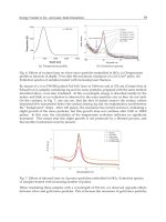
(a) The logical gates learning curves. (b) The XOR logical gate learning curves.
Fig. 6. Learning curves.
gate. The Spiking FeNeuron model is composed by the input, x
i
(n), by the synaptic weights,
ω
i
(n), passing by the RC filters. The result is applied to the ferroelectric capacitor (ξ(.))
performing the output of the model. The phenomenon of the hysteresis loop is used to act as
the the activation function. Using one side of the hysteresis that can be easily simulated as an
error function. The simplicity of the Integrate-and Fire (IF) model is a good advantage. Others
models, as quadratic IF, IF with adaptation, integrate- and-fire-or-burst and resonate-and-fire
are extension and improvement of the integrate-and-fire model. These models are worried
in capture the firing dynamics of real neurons (Janardan and Indranil, 2010). The main focus
of this work is to generate a model that is able to compute and to be applied in engineering
problems with a single neuron model and later with a network of neurons.
Parameters AND NAND OR NOT XOR
Weights (ω
ij
) 0.48/0.48 -0.39/0.69 0.98/0.88 0/-1 0.568/-0.255
Decay constants (τ
ij
) 0.01/0.01 0.01/0.01 0.01/0.01 0.01/0.01 0.01/0.01
Learning rate (γ) 0.01 0.01 0.01 0.01 0.01
Table 1. Parameters of the Spiking FeNeuron.
5.3 Realization of the adaptive logic circuits
In this work the boolean logical gates are simulated by the Spiking FeNeuron showed in
section 5.2. The logical gates are in turn used to construct flip-flop circuits and the flip-flop
circuits are used to construct counters, shift-registers and adders. The logical gates, therefore,
are used as the basic building blocks for all of the digital circuits and their purpose is to control
the movement of binary data and instructions.
5.3.1 Design of the clock
All digital systems use a master timing signal called clock. This two state timing signal is
usually generated from an analog source and may be digitally tuned to meet frequency and
phase requirements. For the Spiking FeNeuron CPU, the clock was generated from an adapted
XOR ring oscillator. A very simplified version of this oscillator is presented as the first stage of
the frequency divider in 5. Here, the input A is tied to logic 1 thereby creating an inverter. The
output of the inverter is then feedback to input B. The frequency of the oscillator will depend
242
Ferroelectrics - Applications
Adaptive Boolean Logic Using Ferroelectrics Capacitors as Basic Units of Artificial Neurons 13
Fig. 7. The Spiking FeNeuron (SFeN) logical gates symbols and the test vectors after training.
on the delay of the feedback signal from the input to the output. Additional adapted XOR
gates can be connected in scries to this one to some higher odd number to obtain the desired
frequency of operation. As an observant reader may have noticed, a Spiking FeNeuron NOT
gate could have been used in place of the Spiking FeNeuron XOR gate to derive the same
results. The choice of the Spiking FeNeuron XOR gate does not provide any additional
benefits over Spiking FeNeuron NOT gate but goes further to demonstrate the exibility of
the Spiking FeNeuron logic. In standard CMOS logic, the NOT gate is almost always the
only choice of a logic component for a ring oscillator due to its few transistor count of two.
Compared to the 16-transistor count for a typical CMOS XOR gate, the area and ultimately cost
savings in silicon makes the CMOS NOT gate the prime choice. In Spiking FeNeuron logic,
however, each of the gates is derived from a single neuron trained to perform its function,
thereby allowing tremendous area savings in hardware.
5.3.2 Design of the frequency divider circuit
A multi-stage frequency divider circuit can be implemented using addition and Spiking
FeNeuron XOR gates. This circuit takes a clock as an input and provides three outputs
with frequencies that are a divide by 2, by 4, and by 8 of the frequency of the input signal.
The design schematic is presented together with the output waveform in Figure 8. On the
schematic, CLK is the input clock signal, Y2 is the divide-by-2 output, Y3 is the divide-by-4
output, and Y4 is the divide-by-8 output.After training all of the gates, a function called
Spiking FeNeuron was created which has two inputs: data vector and the option to select
the desired logical gate required to perform a desired function. The output is the result from
the selected gate.
5.3.3 Design of the D-type flip-flop
The D-type flip-flop is basically a SET-RESET latch with a small circuit modification. On the
rising edge of the clock, the D input is latched to the output Q. The Spiking FeNeuron flip-flop
logic circuit is shown in Figure 9. A test vector was generated to test the flip-flop in the
example 1.
243
Adaptive Boolean Logic Using Ferroelectrics Capacitors as Basic Units of Artificial Neurons
14 Will-be-set-by-IN-TECH
Fig. 8. The block diagram of the frequency divider with waveform.
MATLAB FUNCTION
function output
= dff(data,clk)
data - input vector
clk - vector
output - response vector
EXAMPLE 1:
x
= [001110101]
clk
= [010101010]
output
= dff(x,clk)
output
= [000100000]
Fig. 9. The block diagram of D-flip-flop.
5.3.4 Design of the shift-register
A shift register is constructed using the flip-flop as shown in Figure 10. The shift register is a
storage register that will move or shift the bits of the stored word either to the left or the right.
The simulation of the Serial-In, Serial-Out (SISO) shift register is shown in example 3 with a
test vector. The test vector with a 4-bit word [0110] is being applied to the shift registers input.
The initial state of the shift register flip-flop output is 0. After the first clock pulse, the data
stored is shifted one position to the right and the first bit of the applied serial word is shifted
to the first position of the shifter register. After four clock pulses all the input data will be
stored in the shift register. The summary of the test vector is shown in example 2.
244
Ferroelectrics - Applications
Adaptive Boolean Logic Using Ferroelectrics Capacitors as Basic Units of Artificial Neurons 15
MATLAB FUNCTION
function output
= shiftreg(data)
data - input vector
clk - vector of the clock is generated inside the code
output - response vector
EXAMPLE 2:
output
= shiftreg([1 0 0 1])
output
= [00001000]
Fig. 10. The block diagram of the shift-register.
5.3.5 Design of the ALU
The ALU was construct using half-adder and full-adder circuits. The half-adder circuits were
constructed using Spiking FeNeuron XOR and AND logic gates. The design schematic is
presented on the right side of the Figure 11 where nodes A and B are the half-adder inputs,
and S and carry denote the sum and the carry output signals respectively. The full-adder
circuits were constructed from Spiking FeNeuron half-adders and Spiking FeNeuron logic
gates. The design schematic is shown on the left side of the Figure 11 where A, B and CI
represent the input and carry-in signals respectively. S and carry are the sum and carry
outputs respectively. The full-adder was simulated for proper functionality. The results of
this simulation are presented in example 3.
MATLAB FUNCTION
function [s,carryout]
= fadder(data1,data2,carryin)
data1 - input vector
data2 - input vector
carryin - input of the carry
s - response vector of the sum
carryout - carry output
EXAMPLE 3:
data1
= [1001]
data2
= [1111]
[s, c]= f adder(data1, data2, 0)
s = [1000]
c
= 1
5.3.6 Design of a simple neural CPU
The Central Processing Unit contains an arithmetic-logic unit (ALU), a con- trol unit, and the
registers for storage and manipulation of the data. The design of the CPU contains the ALU,
a 32-bit 8x8 memory designed from Spiking FeNeuron D flip-flops. The system configuration
of the CPU is shown on Figure 12. Information on the system bus which comprise CPU,
memory control and data bhts was simulated with the use of switches. The binary instructions
include memory and register access commands as well as ALU operational commands. The
245
Adaptive Boolean Logic Using Ferroelectrics Capacitors as Basic Units of Artificial Neurons
16 Will-be-set-by-IN-TECH
Fig. 11. The block diagram of the full adder.
microcode structure is shown on Table 2.
An example of some results for the instructions given to the CPU with 8 bits data is shown
(Guerreiro et al., 2008).
Fig. 12. The block diagram of the neural CPU.
Parameters Name
CA R/W operation memory
CB R/W operation register
MandN Memory Selector
CR Register Selector
3/2/1/0 Data
Table 2. The microcode structure.
246
Ferroelectrics - Applications
Adaptive Boolean Logic Using Ferroelectrics Capacitors as Basic Units of Artificial Neurons 17
6. The Model of the FePerceptron in an FPGA
Now, this work is going to show the implementation of the FePerceptron model in a FPGA.
For this implementation we are going to use the DSP builder tool of Altera Corporation.
The DSP Builder technology allows you to go from system definition/simulation using
the industry-standard the MathWorks/Simulink tools to the neuron implementation. The
DSP Builder Signal Compiler block reads Simulink Model Files (.mdl) that are built
using DSP Builder and MegaCore½o blocks and generates VHDL files and tool command
language (Tcl) scripts for synthesis, hardware implementation, and simulation. The DSP
builder automatically generate timing-optimized register transfer level (RTL) code based on
high-level Simulink design descriptions (Altera, 2011).
In this way, first we developed the block diagram of the Simulink model of the FePerceptron
which is shown in the Figure 13. The model is composed by the inputs, in this case two inputs
as required by a Boolean logic gate, and the weights that were generated by the simulations
in Matlab. After that the signal is summed and the output is generated passing the signal
through the activation function that is implemented by the hystheresis of the FeCapacitor.
The Figure 13 shows the implementation of the AND gate, for the other gates we only have
to change the weights values, the same structure is used. The Table 3 shows the result of the
simulations for the gates. Each gate is tested with the input vectors (Data1, Data2) and the
output is seen by the display in Figure 13.
Fig. 13. The block diagram of the FePerceptron in Simulink (DSP Builder) for AND gate.
Data1 Data2 Display(AND) Display(NAND) Display(OR) Display(NOR)
0 0 0 1 0 0.9961
0 1 0 0.9961 0.9973 0
1 0 0 0.9961 0.9973 0
1 1 0.9961 0 1 0
Table 3. The true table simulated by the simulink model of the FePerceptron.
The Simulink model then is converted to the RTL level code. Since the RTL level has a lot of
details is not possible to show all in this work, more details can be found (VHDL, 2011).
247
Adaptive Boolean Logic Using Ferroelectrics Capacitors as Basic Units of Artificial Neurons
18 Will-be-set-by-IN-TECH
7. Conclusion
The FeCapacitors have been embedded into LSIs as Ferroelectric Random Access Memory
(FeRAM) and their reliability data have been accumulated for a long time. The capacitors
are high impedance device, and it is an advantage for low power consumption, besides the
configuration can be changed after packaging.
Thinking on this scenario, the FeCapacitor was choosen to be used in this work. It uses
the phenomenon of the hysteresis loop of the FeCapacitor as the activation function for the
artificial neuron models. We developed two models, the FePercetron and the FeSpiking
Neuron Model, both models were first simulated in Matlab, and used to simulated the boolean
functions. Since the FePerceptron were not able to simulated the XOR gate with a single
neuron, because of the Perceptron characteristics. We were motivated to implement the
FeSpiking that was based in the Extended Spiking Neuron Model and all logic gates were
simulated, including the XOR. So, an adaptive simple CPU were developed, with simple
logical circuits implemented, as registers, ALU, D-flip-flop as shown in section 4.
The FePerceptron and the FeSpiking Neuron Model presented the advantaged of being
soft-programmable. This is accomplished by only adjusting the weight values of the synaptic
connections without the need of changing all the architecture. It was firstly implemented by
software verifying the success of the models.
From both models, first we chose the FePerceptron to be implemented in hardware because
of the simplicity of the model. For this implementation we used the DSP builder tool of
Altera Corporation. The DSP Builder Signal Compiler block read Simulink Model Files
developed(.mdl) that were built using DSP Builder blocks and generated the VHDL files and
the RTL level. This is the first step to develop more complex model as the FeSpiking Neuron
Model, since the basic unit of the activation function (FeCapacitor) is already developed.
As hardware implementations, this model brings the contribution of being very simple, can
save in silicon area, with low power consumption and being reconfigurable in two degrees of
freedom, not only as characteristics intrinsic of the FPGA, but with the reconfigurability of the
boolean gates. It is only necessary to change the values of the weights and the output is going
to change to be the desired gate.
8. References
Altera Corporation. Diponível em: www.altera.com/products/dsp/dsp-builder.html.
Acessado em: 10 de fevereiro de 2011.
Beiu, V.; Quintana, J. M.; Avendillo, M. J. (2003). VLSI Implementations of Threshold Logic - A
Comprehensive Survey, Vol. 14, pp. 1217-1243.
Bermak, D.; Martinez, D. A compact 3-D VLSI classifier using bagging threshold network ensembles
IEEE Transactions on Neural Networks 14(5) (2003) 1097â
˘
A¸S1109.
Brown, B.; Yu, X.; Garverick, S. A Mixed-mode analog VLSI continuous-time recurrent neural
network Proceedings of International Conference on Circuits, Signals and Systems,
2004,pp.104â
˘
A¸S108.
Chen, Z.; Haykin, S; Becker, S. Theory of monte carlo sampling-based alopex algorithms for neural
networks. Proceedings of IEEE International Conference on Acoustics, Speech, and
Signal Processing, pp. 17-21.
Dias, Fernando Morgado; Antunes, Ana; Manuel Mota, Alexandre. Artificial neural networks: a
review of commercial hardware Engineering Applications of Artificial Intelligence, v.17
n.8, p.945-952, December, 2004
248
Ferroelectrics - Applications
Adaptive Boolean Logic Using Ferroelectrics Capacitors as Basic Units of Artificial Neurons 19
Duong, T.A. Cascade error projection: an efficient hardware learning algorithm Proceedings of the
IEEE International Conference on Neural Networks, vol. 1, Perth, Australia, 1995, pp.
175-178.
Duong, T.A.; Stubberud, A.R., Convergence analysis of cascade error projection: an efficient
hardware learning algorithm. International Journal of Neural System. v10 i3. 199-210.
D’Acierno, A. Back-propagation learning algorithm and parallel computers: the CLEPSYDRA
mapping scheme. Neurocomputing. v31. 67-85.
Fakhraie, S.M.; Farshbaf, H; Smith, K.C. Scalable closed-boundary analog neural networks. IEEE
Transactions on Neural Networks. v15. 492-504.
Glesner, M.; Poechmueller, W. Neurocomputers: An Overview of Neural Networks in VLSI. 1994.
Chapman and Hall, London.
Guerreiro, Ana Maria GuimarÃˇces; McMillan, Larry; Araujo, Carlos A Paz de. Adaptive Logic
Synthesis by Ferroelectric Spiking Neuron Circuits. Integrated Ferroelectrics, v. 100, p.
238-253, 2008.
Haykin, S. (1998). Neural Networks: A Comprehensive Foundation. Prentice Hall, 2nd Edition.
Heemskerk, J. Overview of neural hardware Neurocomputers for Brain-Style Processing, Design,
Implementation and Application, 1995.
Kumar,V.;Shekhar,S.;Amin,M.B.A Scalable Parallel Formulation of the Backpropagation
Algorithm for Hypercubes and Related Architectures IEEE Transactions on Parallel and
Distributed Systems, v.5 n.10, p.1073-1090, October 1994.
Ienne, Paolo; Cornu, Thierry; Kuhn, Gary. Special-purpose digital hardware for neural networks: an
architectural survey Journal of VLSI Signal Processing Systems, v.13 n.1, p.5-25, Aug.
1996.
Jabri, Marwan; Flower, Barry. Weight perturbation: An optimal architecture and learning technique
for analog vlsi feedforward and recurrent multilayer networks. Neural Computation, v.3
n.4, p.546-565, Winter 1991.
Janardan, Misra; Indranil, Saha. Artificial neural networks in hardware: A survey of two decades
of progr ess. Journal Neurocomput. vol 74. 2010. ISSN: 0925-2312. Elsevier Science
Publishers B. V.
Kung, S.Y. Digital Neural Networks Prentice-Hall, Upper Saddle River, NJ, USA, 1992.
Lehmann, Torsten; Bruun, Erik; Dietrich, Casper. Mixed an alog/digital matrix-vector multiplier
for neural network synapses Analog Integrated Circuits and Signal Processing, v.9 n.1,
p.55-63, Jan. 1996.
Lamela, H.; and Ruiz-Llata, M. Optoelectronic neural processor for smart vision applications.
Imaging Science Journal. v55 i4. 197-205.
Lenne, P. Digital hardware architectures for neural networks Speedup Journal 9(1)(1995)18â
˘
A¸S25.
McCulloch, W. S.; Pitts, W. (1943). A logical calculus of the ideas immanent in nervous activity,
Bull. Math. Biophysiol., vol. 5, pp. 115-133.
Mead, C. Analog VLSI and Neural Systems Addison-Wesley,Boston,MA, USA, 1989.
Miller, S. L.; Schwank, J. R.; Nasby, R. D.; and Rodgers, M. S. (1991). Modeling Ferroelectric
capacitor switching with asymmetric nonperiodic input signals and arbitrary initial
conditions. J. Appl. Phys., vol. 70, no. 5, pp. 2949-2860.
Moerland, P.D.; Fiesler, E; and Saxena, I. Incorporation of liquid-crystal light valve nonlinearities
in optical multilayer neural networks. Applied Optics. v35. 5301-5307.
Nedjah, Nadia; Mourelle, Luiza de Macedo. Reconfigurable hardware for neural networks: binary
versus stochastic Neural Computing and Applications, v.16 n.3, p.249-255, May 2007.
249
Adaptive Boolean Logic Using Ferroelectrics Capacitors as Basic Units of Artificial Neurons
20 Will-be-set-by-IN-TECH
Patnaik, L.M.; Rao, R.N. Parallel implementation of neocognitron on star topology: theoretical and
experimental evaluation. Neurocomputing. v41. 109-124.
Rà ˛ak, à ˛Adà ˛am; Soøss, Balà ˛azs Gergely; Cserey, GyÃ˝urgy. Stochastic bitstream-based
CNN and its implementation on FPGA International Journal of Circuit Theory and
Applications, v.37 n.4, p.587-612, May 2009.
Rosemblatt, F. (1958). The perceptron: A probabilistic model for information storage and organization
in the brain. Psych. Revue, vol. 65, pp. 386-408.
Sheikholeslami, A.; Gulak, P. Glenn (1997). A Survey of Behavioral Modeling of Ferroelectric
Capacitors. IEEE Trans. on Ultrasonics, Ferroelectrics, and Frequency Control vol. 44,
no. 4, pp. 917-923.
Schmid, A.; Leblebici, Y.; and Mlynek, D. A mixed analog digital artificial neural network with on
chip learning. IEE Proceedings-Circuits, Devices and Systems. 2004. v146. 345
Schrauwen, B.; D’Haene, M. Compact digital hardware implementations of spiking neural networks
J. Van Campenhout (Ed.), Sixth FirW Ph.D. Symposium, 2005, in CD.
Shibata, T.; Ohmi, T. (1991). An intelligent MOS transistor featuring gate-level weighted sum
and threshold operations. Technical Digest of International Electron Devices Meeting,
Washigton DC, pp. 919-922.
Smieja, F. J. Neural network constructive algorithms: trading generalization for learning efficiency
Circuits, Systems, and Signal Processing, v.12 n.2, p.331-374, 1993.
Sundararajan, N.; Saratchandran, P. Parallel Architectures for Artificial Neural Networks:
Paradigms and Implementations IEEE Computer Society Press, Los Alamitos, CA, 1998.
Strey, Alfred; Avellana, Narcis. A New Concept for Parallel Neurocomputer Architectures
Proceedings of the Second International Euro-Par Conference on Parallel
Processing-Volume II, p.470-477, August 26-29, 1996.
Tokes, S.; OrzÚ, L.; Vr, G.; Roska, T. Bacteriorhodopsin as an analog holographic memory for joint
fourier implementation of CNN computers Technical Report DNS-3-2000, Computer and
Automation Research Institute of the Hungarian Academy of Sciences, Budapest,
Hungary, 2000.
Valle, M. Smart Adaptive Systems on Silicon. 2005. Springer, Dordrecht, The Netherlands.
Verleysen, Michel; Thissen, Philippe; Voz, Jean-Luc; Madrenas, Jordi. An Analog Processor
Architecture for a Neural Network Classifier, IEEE Micro, v.14 n.3, p.16-28, June 1994.
VHDL. Diponível em: ftp://alan: Acessado em: 20 de fevereiro de
2011.
Zhu, J.; Sutton, P. FPGA implementations of neural networks-a survey of a decade of progress.
Field-Programmable Logic and Applications, vol. 2778. pp. 1062-1066.
Yang, F.; Paindavoine, M. Implementation of an RBF neural network on embedded systems: real-time
face tracking and identity verification. IEEE Transaction on Neural Networks. v14 i5.
1162-1175.
250
Ferroelectrics - Applications