Ferroelectrics Characterization and Modeling Part 2 docx
Bạn đang xem bản rút gọn của tài liệu. Xem và tải ngay bản đầy đủ của tài liệu tại đây (3.46 MB, 35 trang )
Near-Field Scanning Optical Microscopy Applied to the Study of Ferroelectric Materials
25
2. Experimental details of the AFM
This section consists of a brief introduction to the AFM technique followed by the
description of the commercial electronics used by experimental set-up in this work. As a
peculiarity, we can mention that the SPM techniques were proposed many years ago, but
they could not be developed until the 80s because of such techniques required positioning
systems of great precision. Nowadays, thanks to existence of piezoelectric positioners and
scanners, the tip-sample distance can be controlled with a precision in the order of the
Angstrom. As a result, the AFM resolution is limited by other effects different from relative
tip-sample motion precision.
2.1 The AFM
The basis of the AFM is the control of the local interaction between the microscope probe
and the material surface. The probe, usually a silicon nano-tip, is located at the end of a
micro-cantilever. To obtain images of the sample topography, the distance between the tip
and the sample is kept constant by an electric feedback loop. The AFM working principle
varies depending on the operation mode. In the case of ferroelectric surfaces the most
used method is the “non-contact mode” due to the fact that such mode allows the
simultaneous measurement of electrostatic interactions (Eng et al., 1998, 1999). Working in
non-contact mode, an external oscillation is induced to the cantilever by means of a
mechanical actuator. In our commercial AFM (Nanotec Electronica S.L.) a Schäffer-
Kirchoff
®
laser is mounted in the tip holder for monitoring the cantilever motion. The
laser beam (<3mW at 659 nm wavelength) is aligned in order to be focused in the
cantilever (see Fig. 2a) impinging the reflected light in a four-quadrant photodetector (Fig.
2b). In this way, the cantilever oscillation can be determined by comparison between the
signals measured in the four diodes of the detector. If the frequency of the external
excitation is close to the resonant frequency of the cantilever (i.e. 14-300 kHz), the
oscillation amplitude generates an analogical signal that can be measured using lock-in
techniques (synchronous amplification). Far away of the sample surface, the dynamics of
the cantilever-tip system can be approached to a forced (driven) harmonic oscillator. But if
the probe is located close to the sample (in the range of 10-25 nm), the tip is exposed to the
surface interaction and the harmonic oscillator is damped by van der Waals forces. Since
the damping force is determined by the position of the tip with respect to the sample, the
oscillation amplitude also depends on such distance. For this reason, the feedback control
maintains the oscillation amplitude in order to keep constant the tip-sample distance
during the scan. Therefore, as the feedback correction consists in a displacement of the tip
along the Z-axis, the sample roughness is reproduced by the tip motion which is
monitored to obtain AFM topography images.
Nowadays, the AFM tip fabrication process has received much attention in order to obtain
an enhancement of the microscope resolution, due to the fact that the tip size and shape
determine the interaction forces. In addition, the tip can suffer other modifications like
cobalt coating for MFM probes or doping for local current measurements. In this sense,
several AFM advanced techniques can be performed using the appropriate tip in order to
obtain electrostatic or magnetic information of the surface with an important resolution
enhancement. We describe below the modifications introduced in our commercial AFM
(electronics) for obtaining optical information of the sample surface.
Ferroelectrics - Characterization and Modeling
26
Fig. 2. (a) AFM scheme. (b) four-quadrant photodetector. (c) Standard Silicon probe
(PointProbePlus, Nanosensors
TM
).
2.2 The NSOM
The NSOM is a SPM technique whose resolution is limited by the probe parameters and which
allows the microscope user to obtain the optical and the topography information
simultaneously (Kawata, Ohtsu & Irie, 2000; Paeleser & Moyer, 1996). This fact makes NSOM a
valuable tool in the study of materials at the nanometer scale by refractive index contrast,
surface backscattering or light collection at local level.
Our NSOM is based on a tuning-fork sensor head, whose setup (Fig. 3a) is similar to that of
a commercial AFM working in dynamic mode, but in this case, the standard silicon probe is
replaced by a tip shaped optical fibre (Fig. 3b). The probe is mounted on a tuning pitch-fork
quartz sensor (AttoNSOM-III from Attocube Systems AG), which is driven at one of its
mechanical resonances, parallel to the sample surface Fig. 3c. In a similar way than at AFM,
this vibration is kept constant by the AFM feedback electronics in order to maintain the tip-
sample distance. The tuning fork sensor is controlled with the feedback electronics and data
acquisition system used in our commercial AFM (Dulcinea from Nanotec S.L.). Simply the
AFM tapping motion is substituted by the shear force oscillation of the tuning-fork quartz.
Our NSOM is used in illumination configuration under a constant gap mode (Figure 3a) in
order to obtain transmission images, by measuring the transmitted light using an extended
Near-Field Scanning Optical Microscopy Applied to the Study of Ferroelectric Materials
27
silicon photodetector located on the sample holder. For this purpose, the excitation light
(laser diode) is delivered through a 2x2 fibre beam splitter using one of the coupler inputs
(I1). One of the beam splitter outputs (O1) is connected to the fibre probe while the other
output (O2) can be used to control the excitation power. Finally, the light reflected at the
sample surface is guided to another photodetector thought the remaining beam splitter
input (I2). The electrical signals (reflection and transmission) produced by both
photodetectors are coupled to a low noise trans-impedance pre-amplifier and processed by
the AFM image acquisition system (i.e. a digital sample processor). Even in previous works,
the comparison of transmission and reflection images has been determinant for the
understanding of the experimental results; in ferroelectric materials we are going to focus
our attention on transmission images exciting the sample with 660nm wavelength.
Fig. 3. (a) NSOM illumination scheme, pictured taken from (Canet-Ferrer et al., 2007). (b)
NSOM probe prepared in our lab: aluminium coated tip. (c) The NSOM probe mounted on
one of the arms of a tuning fork.
Ferroelectrics - Characterization and Modeling
28
Fig. 4. Different kinds of near-field optical signals. All of them could be measured in
illumination configuration.
3 Theoretical approach
3.1 2D model for NSOM optical transmission
Optical images acquired by NSOM can be treated by means of theoretical calculations in
order to extract all the information they contain, but unfortunately, there is not a friendly
analytical expression to describe transmitted signal under near-field conditions through a
sample whose surface usually exhibits a random roughness. In this sense, the task of
reproducing a refractive index profile of surface and sub-surface objects from optical
transmission contrasts requires a great calculation effort to obtain accurate results. In
addition, the surface characteristics of ferroelectric materials present other difficulties to
perform quantitative analysis of the optical contrasts since some parameters are not exactly
known, as the density of doping atoms, diffusion mechanism or strain maps. Fortunately,
sometimes it is enough discriminating the domain structure for achieving valuable
information for the optimization of the material applications. In this sense, NSOM
transmission images can be easily interpreted if we take the next considerations in a 2D-
model: (i) the sample is considered a flat surface composed by two different layers whose
thicknesses would depend on the sample characteristics; (ii) an effective refractive index is
considered at the upper-layer depending on the tip position (i.e. at each pixel of the image),
while the second layer present an homogeneous refractive index; and (iii) the
electromagnetic field distribution in the plane of the probe aperture is approached to a
Gaussian spatial distribution with a standard deviation σ ~ 80 nm (i.e., approximately the
tip aperture diameter), as illustrated in Fig. 5(a). Taking into account these considerations
the light transmission contrasts can be simulated as follows.
Near-Field Scanning Optical Microscopy Applied to the Study of Ferroelectric Materials
29
Fig. 5. (a) Near-field probe close to the feedback range. The optical intensity on the aperture
plane is approached to a Gaussian field distribution. (b) Scheme of the main interfaces
considered in our 2D simulation. Working at constant gap mode the tip is maintained at a
distance, d, of a few nanometers. The upper layer is considered as a flat film (2λ thickness)
with an average refractive index, n
eff
(x, y), which depends on the position. Below the
channel upper-layer (at a far-field distance), we find the homogeneous media (the pictures
are not at a correct scale in all dimensions). (c) 2D representation of the near-field probe (80
nm) in feedback range close to a scatter object larger than the wavelength. The relative
position of the propagating light cone and the sphere immersed in the upper layer depends
on their optical convolution. Therefore, a different effective refractive index n
eff
is expected
for each pixel of the NSOM tip scan. Figure taken from (Canet-Ferrer et al., 2008).
Firstly, the electromagnetic field distribution coming from the optical probe is decomposed
into its angular spectrum.
2
()
2
(, 0)
x
kx
Exz
ce
βπ
β
βπ
=
=−
==
(1)
The excitation light is developed into a linear combination of plane-waves simplifying the
calculations since the transmission for each component can be treated separately (Nieto-
Vesperinas, 2006). Such decomposition consists of a 2D-Fourier transform of the
propagating and evanescent plane waves:
2
1
()
2
2
x
x
kx
cdx
ee
β
σ
σπ
−
−
=
(2)
Ferroelectrics - Characterization and Modeling
30
where k
x
is the projection of the wavenumber along the X axis and β= k
z
is the
wavenumber corresponding to the propagation direction, see Fig. 5a. First, the plane-waves
propagate in free space from the tip to the sample surface (i.e. a typical air gap of
10 nm under feedback conditions, represented by the distance “d” in Fig. 5b). At this point,
reflection at the surface (and later at rest of interfaces) is considered according to
condition (i) and beneath it, the plane-wave components propagate through an
inhomogeneous medium (the sample upper-layer). As an approach, the light
transmission can be calculated by an effective medium approximation (condition ii),
due to the variations in the refractive index during the light propagation. The
transmission of each plane-wave at the sample surface is determined through the
boundary conditions of Maxwell equations between two dielectric media (Hecht E. &
Zajac, 1997):
2
()
() ()
2
()
(, )
[]
(, )
eff
eff eff
i
Exzd
Tt
Exzd
β
ββ
β
=
==
=
(3)
Let notice that, if a suitable reference plane is chosen for the angular spectrum
decomposition, the transmission for each incident plane wave, E
i
(β), would correspond to
the Fresnel coefficient at the incidence angle
θ
i
= Arcsin( kx /n
air
k
0
) (4)
which is related with the β-wavenumber by
β
i
2
= n
air
k
0
2
- k
x
2
(5)
while the angle of the transmitted wave can be directly obtained from the Snell’s law (Hecht
E. & Zajac, 1997)
sin sin
air
eff i
eff
n
Arc
n
θθ
=
(6)
Once the light traverses the upper-layer it suffers a second reflection (and refraction) at the
interface with the homogeneous refractive index material. Expressions like (3)-(6) can be
deduced again to determine the transmission coefficients through the second layer, but, in this
case, the incidence angle corresponds to the inclination of waves in the effective media (θ
eff
),
2
()
() ()
2
()
(, 2)
[]
(, 2)
sl
sl sl
eff
Exzd
Tt
Exzd
β
ββ
β
λ
λ
=+
==
=+
(7)
Before reaching the photodetector in transmission configuration, the light arrives at the
substrate-air interface which introduces a last transmission coefficient:
2
()
() ()
2
()
(,)
[]
(,)
air
air air
sl
Exz
Tt
Exz
β
ββ
β
==
(8)
Near-Field Scanning Optical Microscopy Applied to the Study of Ferroelectric Materials
31
Notice that in this interface the plane-waves arriving with an incidence angle larger than the
critical one for total internal reflection (θ
tir
) will not contribute to the optical signal. At the
same time, the finite dimensions of the detector must be also taken into account since the
numerical aperture (NA) of the photodiode could also introduce another limiting angle.
Having both facts into account, it is defined the cut-off wave-number, β
c
= NA k
0
, like the
maximum wave-vector of the propagated light, which is equivalent to a maximum receiving
angle θ
c
by the relation β
c
2
= n
i
k
0
(1-sin2θ
cut
) (Hecht B. et al., 1998), limited by either the
detector or total internal reflections. As a result, the expression for the light arriving to the
detector can be written as:
2
()()()
()
c
c
air
sl eff
TTTTc
β
β
βββ
β
−
=
(9)
It is worth noting that during the wave-front propagation the Gaussian beam coming
from the NSOM suffer a great divergence. Therefore, if the upper-layer is extended
beyond the near-field (e.g., upper-layer up to 2λ thick) the electromagnetic field
distribution at the interface with the second layer is considerably extended. In these
conditions the second layer can be considered as a homogeneous media with a constant
refractive index, satisfying condition (ii). On one hand, the precision estimating the values
for the thickness of layers are not critical for the semi-quantitative discussion aimed in
this work since such parameter mainly affects the phase of the propagating fields.
Nevertheless, it is necessary to point out that the real thickness of each layer must be had
into account in certain cases, like in very thin films (thickness << λ) or stratified media
(with possible optical resonances) for which multiple reflections are expected to
contribute significantly to the transmitted field. In those cases, it is recommended to
calculate the transmission coefficients having into account the phase component (Chilwell
& Hodgkinson, 1984; Yeh, Yariv & Hong, 1977). On the other hand, samples which consist
of a photonic device (like waveguides, beam splitters, optical filters, amplifiers, etc)
would requires the decomposition of the sample profile in multiple layers with the aim to
distinguish between the different interfaces delimiting the device geometry. For instance,
in Ref. (Canet-Ferrer et al., 2008) we simulated the refractive index contrast produced by
solid phases present on the surface of a channel waveguide in lithium niobate. In that
case, the presence of the waveguide was considered by introducing an additional layer.
3.2 Effective media approach
It is necessary to point out that according to condition (ii) the effective refractive index is
going to depend on the upper-layer local composition. Therefore, a different refractive index
must be considered at each measuring point (at each pixel of the transmission image).
Figure 2(c) illustrates how the local refractive index could be estimated in a general case. It is
based on the effective medium theory (EMT), which during last years has been successfully
applied to ferroelectric materials (Sherman et al., 2006). The effective dielectric constant ε
eff
(and therefore the refractive index) for a N-dimensional material (in our case we limit the
model to N=2) comprising inclusions of other material with permittivity ε’ and a filling
factor p with respect to the host medium (in our case the upper-layer) with a permittivity ε
up
is given by (Bruggeman, 1935):
Ferroelectrics - Characterization and Modeling
32
2
1
{( 1) ' ( 1 )
2( 1)
[( 1) ' ( 1 ) ] 4( 1) ' }
eff up
up up
Dp D Dp
D
Dp D Dp D
εεε
εεεε
=−+−−
−
+−+−− +−
(10)
At each pixel we consider the area corresponding to the light cone cross-section limited by
the detector and, consequently, the filling factor is determined with respect to such area, as
indicated in figure 2c (i.e. the isosceles triangle determined by β
c
). As a result, the estimation
of the refractive index when scanning the surface of the upper layer by the NSOM tip is
based on the convolution between the propagating light cone and the objects producing
optical contrast. Assuming that both the hidden object and the host matrix are
homogeneous, the effective refractive index profile becomes proportional to the spatial
convolution along the scan direction of the cone of light and the scatter depicted in Fig. 5c.
Therefore the optical contrast can be directly interpreted by means of geometrical
considerations (Canet-Ferrer et al., 2008). Unfortunately, dielectric profile usually presents a
Gaussian shape at the ferroelectric domain walls and consequently the effective dielectric
constant cannot be determined by means of Eq. 10. In that case the refractive index at the
upper layer pixels must be evaluated by means of
(,)
S
eff
S
x z dxdy
dxdy
ε
ε
=
(11)
Where ε(x,z) represents the dielectric constant as a function of the position and S is the
surface defined by the light cone. Eq. 11 can be easily evaluated for the scanning situation
depicted in Fig. 6. But in this case the index profile is not a bivaluated function; therefore the
effective refractive index and the optical contrast would not be directly related by the
respective spatial convolution. Having this fact into account, in the next section we are
going to propose and alternative way to extract information from transmission images.
Fig. 6. At the top, it is depicted the NSOM tip in two different points: i) the domain wall and
ii) the center of a wide ferroelectic domain. It is also marked the evaluation area as
shadowed triangles. At the bottom, the refractive index profile is represented.
Near-Field Scanning Optical Microscopy Applied to the Study of Ferroelectric Materials
33
4. Characterization of the domain walls in potassium niobate.
In this section we are going to study the refractive index profile induced by ferroelectric
domains in a potassium niobate (KNbO
3
) bulk sample performed by means of NSOM. The
potassium niobate KNbO
3
(KNO) belongs to the group of perovskite-type ferroelectric
materials, like the Barium Titanate. At room temperature, the KNO has an orthorhombic
crystal structure with space group Amm
2
and presents natural periodic ferroelectric
domains with 180º spontaneous polarization (Topolov, 2003). Extensive theoretical and
experimental studies have been performed on this material since the discovery of its
ferroelectricity (Matthias, 1949), due to its outstanding electro-optical, non-linear optical
and photorefractive properties (Duan et al., 2001; King-Smith & Vanderbilt, 1994 ;
Postnikov et al., 1993; Zonik et al., 1993). In the last decade, the KNO has received much
attention due to the relation existing between the piezoelectric properties and the domain
structures. However, many of these properties are not well understood at the nanometer
scale. From the technological point of view some ferroelectric crystals, as KNO, form
natural periodic and quasi-periodic domain structures. The motion of such domain wall
plays a key role in the macroscopic response. For this reason, a variety of experimental
techniques such as polarizing optical microscopy, anomalous dispersion of X-rays, Atomic
Force Microscopy (AFM), Scanning Electron Microscopy (SEM) and Transmission
Electron Microscopy (TEM), have been used to study the electrostatic properties of the
KNO domains (Bluhm, Schwarz & Wiesendanger, 1998; Luthi et al., 1993; Yang et al.,
1999). From the different techniques employed in the domain structure characterization,
the Electrostatic Force Microscopy (EFM) and Piezoelectric Force Microscopy (PFM) have
been turned into useful practices (Labardi, Likodimos & Allegrini, 2000), since such
techniques are based in the electrostatic interaction between the AFM tip and the surface
polarization. But unfortunately both methods present important limitations working with
bulk materials due the huge external electric field required for inducing the mentioned
interaction. As an alternative, the NSOM has been used to demonstrate how the optical
characterization of the ferroelectric domains is able to offer useful information even
working with bulk materials.
The advantage of our NSOM consists of the possibility of acquiring the images with
nanometric resolution, containing the optical information and the topographical features,
simultaneously. In the present sample, our probes reached a resolution better than 100 nm
on the lateral directions and around 1-3 nm in height (in topography). About the optical
images, it can be distinguished two main components contributing to the near-field signal:
i) surface scattering and ii) evanescent waves transformed in propagating waves in the
presence of a refractive index enhancement (Wang & Siqueiros, 1999). In the first case, the
scattering is more important as the light source is closer to the surface; thus scattered
waves mainly contain information about the interaction of the tip with the surface
roughness. On the other hand, information of the local refractive index (effective
refractive index estimated by means of Eq. 11 for the upper layer) is manly contained in
the evanescent waves arriving to the detector. Depending on the ratio between both
contributions the transmission signal could contain topographical features merged with
the optical contrasts (Hecht et al., 1997).
In a previous work the scattering contribution was demonstrated to be considerably
reduced by using a visible light source as excitation (Canet-Ferrer et al., 2007). In addition,
the topography contribution can be even negligible in KNO due to the huge refractive index
Ferroelectrics - Characterization and Modeling
34
contrast in this material. For example, Fig. 7 shows two NSOM images (topography and
transmission) acquired simultaneously. The topography image (Fig. 7a) shows a certain
roughness forming elongated structures with a depth of around 5-7 nm (Fig. 7b) that we
attribute to the sample polishing process. In contrast, the transmission image (Fig. 7c) is
mainly composed by wider optical modulations (Fig. 7d) orientated on a different direction
(with respect to surface features), and thus the optical contrasts cannot be correlated with
topography details. For a better comparison, the profiles extracted from Figs. 7a and 7c
(marked with a grey line) are depicted in Figs. 7b and 7d. It can be changes in the
transmitted light larger than 30-35 mV over an average absolute value for the transmission
intensity around 2 V. Assuming that the observed optical modulations are produced by the
refractive index contrast at the domain walls, the resulting optical contrast would be in the
order of predictions and measurements in pervoskite-type materials (Otto et al., 2004; Chaib,
Otto & Eng, 2002a; Chaib et al., 2002b).
Fig. 7. Topography image (a) and profile along the blue line (b) of a KNO surface. Idem for
transmission image in (c) and (d).
The next step consists of deducing a relation between the measured optical contrast and
the refractive index. On the one hand, close to the domain wall the effective dielectric
constant at the upper-layer is better estimated by means of Eq. 11. On the other hand, the
relation between the optical contrast and the effective refractive index is rather
complicate. For this reason, it would be more helpful to establish simple relations between
the refractive index and the transmission of plane waves composing the Gaussian
excitation beam. For example, the optical contrast (ΔT
(0)
) produced by the normal
incidence component (β=0) as a function of the refractive index change in different points
of the upper layer (Δn) can be expressed as follows:
Near-Field Scanning Optical Microscopy Applied to the Study of Ferroelectric Materials
35
(0)
(0)
(1)
1
Tnn
nn
T
Δ−Δ
=−
+
(12)
being T
(0)
the transmittance of the mentioned plane wave and n the refractive index of the
material at the point of incidence. However, not all the plane waves in the angle range
defined by [-β
c
, β
c
] will contribute to the optical contrast with the same intensity. In fact,
almost 85% of the electromagnetic field intensity is contained at the low inclination
waves, being the normal incidence (β=0) the main amplitude component. In order to
illustrate this fact, in Fig. 8 it is shown the transmittance of a material (with refractive
index 2.2 at the second layer) as a function of the upper-layer effective refractive index.
The calculation is performed by considering that transmitted light is measured through an
extended detector (high NA), which means that β
c
is limited by θ
tir
. Calculated curves
stand for the entire Gaussian excitation field (red line) and for only the contribution of
normal incidence plane wave (blue line). As above suggested, the transmittance of the
electromagnetic field distribution is noticeably influenced by the normal incidence
component. It is also worth mentioning that the transmittance change can be
approximated by a linear behaviour for relatively small index contrast, being the slope of
both curves quite similar in such case. Consequently, even if the approximation of a point-
like light source by a planar wave could seem rough, very close values of (ΔT/Δn) are
expected in both cases.
Fig. 8. Transmittance calculated the entire Gaussian beam (red line) and its normal incidence
component (blue line) through a two layer sample as a function of the upper-layer effective
refractive index. The thickness of each layer is selected according to the real KNO sample
dimensions: 2λ for the upper-layer, 1mm for the second layer.
Thanks to this fact, transmission images can be converted into refractive index images by
means of a simple expression:
(0)
(0)
(1)
1
TT n n
Tnn
T
ΔΔ −Δ
≅=−
+
(13)
Ferroelectrics - Characterization and Modeling
36
where now T is the averaged optical signal of a transmission image and ΔT is the
experimental optical contrast between two different pixels. The details of the calculation
(normalization, numerical aperture effects, tip-sample distances, etc) and its limitations
(related with the domain size) are out of the scope of the present work. However, Eq. 13
represents a very simple and semi-quantitative expression to account for local refractive
index contrasts in a given material, applicable if the component β=0 dominates the
transmittance. As an example, Fig. 9a shows a transmission image acquired under similar
conditions to Fig. 7b, but in another zone of the sample. From Fig. 9a we generate the
corresponding refractive index image (Fig. 9b) by applying Eq. 13. We can associate optical
variations of around 14 mV (with respect to an average background signal of 2V) with
refractive index contrasts of around 3% (with respect to the KNO bulk refractive index n
sl
=
2.2) by comparing a given profile line in both images (Figs. 9c and 9d). Quantitatively, such
a contrast is large as compared to reported values in other ferroelectric materials (Canet-
Ferrer et al., 2006; Lamela et al., 2009; Han et al., 2009). On the other hand, it is in agreement
with respect to the theoretical predictions in Ref. (Chaib et al., 2002b).
Fig. 9. Transmission (a) and the corresponding refractive index contrast image (c) of the
KNO surface. They are accompanied by the corresponding profiles (b) and (d), respectively.
Finally the refractive index images can be used for studying the periodicity and width of the
domains by means of averaging the profiles extracted from many images. After comparing
several zones of the sample surface, it is observed certain dependence of the optical contrast
on the domain width. The results are plotted in Fig. 10a like a scatter cloud where, despite
the dispersion in the experimental data, it is observed a clear tendency to increase the
refractive index contrast with the size of the domains. A priori this result could seem
contradictory, since it is supposed that the larger domains could easily relax the strain at the
Near-Field Scanning Optical Microscopy Applied to the Study of Ferroelectric Materials
37
interfaces. In fact, Chaib et al. calculated the refractive index contrast for different domain
sizes and showing how such contrast become smaller for walls belonging larger domains,
contrary to our observations. Consequently we can conclude there is another effect related
with the domain size influencing the optical contrast measurement. This effect could be
explained attending to the expected refractive index profiles at the domain walls (Fig. 6). For
this purpose, the refractive index images have been fitted to Gaussians profiles, one for each
domain wall. As a result we can conclude that in our sample the domain walls are not
separated enough to observe a fully developed refractive index contrast, as illustrated in Fig.
10b. At the top panel two separated domain walls (red horizontal line) leads to a maximum
optical contrast (blue vertical arrow). At the bottom panel of Fig. 10b, the measured contrast
(and width) is highly reduced when the domain walls get closer. The optical contrasts are
thus underestimated in this case as previously reported (Han et al., 2009).
Fig. 10. (a) Optical contrast as a function of the domain size; (b) effect of proximity between
the domain walls on the optical contrast.
5. Conclusions
The AFM main properties have been described with the aim to approach the reader to the
SPM microscopes. The characteristics of a commercial AFM electronics have been
specified since it is the basis of our NSOM. The NSOM illumination configuration has
been described in order to study ferroelectric materials. Even if EFM and PFM are the
most used techniques to observe electrostatic effects in ferroelectric thin films, NSOM
characterization can offer information on the refractive index changes at the domain
structure. In the near-field images we observe a clear optical contrast at the domain walls
which an average value is around 2% in transmission. These contrasts appear with
negligible effect of the topographic features and presenting certain dependence on the
separation between domain walls. Thanks to the refractive index contrast images, the
average separation between domain walls is found to be around 1.5 μm. Finally, it is
worth noting the fact that NSOM imaging provides the possibility of characterizing bulk
samples, which are inaccessible by EFM or PFM, without a special preparation of the
surface (chemical selective etching, for example), as done to observe periodic domain
structures by standard optical microscopy.
Ferroelectrics - Characterization and Modeling
38
6. Acknowledgements
The main author, J. C F., thanks the Spanish MCI for his FPI grant BES-2006-12300.
7. References
Abbe E (1882) J. Roy. Micr. Soc. 3 300.
Asenjo A, Jaafar M, Navas D & Vazquez M (2006). Quantitative magnetic force microscopy
analysis of the magnetization process in nanowire arrays. J. Appl. Phys. 100 023909.
Bluhm H, Schwarz UD & Wiesendanger R, (1998). Origin of the ferroelectric domain constrast
observed in lateral force microscopy. Phys. Rev. B, 57, 161.
Bruggeman DAG, (1935). "Berechnung verschiedener physikalischer Konstanten von heterogenen
Substanzen", Ann. Phys. 24 636.
Canet-Ferrer J, Martin-Carron L, Martinez-Pastor J, Valdes JL, (2006). Scanning probe
microscopy applied to the study of domains and domain walls in a ferroelectric KNbO
3
crystal. Bol. Soc. Esp. Ceram y Vidrio, 45, 218.
Canet-Ferrer J, Martin-Carron L, Martinez-Pastor J, Valdes JL, Martínez-Pastor, Carvajal JJ &
Diaz F, (2006). Near-field optical and atomic force microscopy studies of a RbTiOPO
4
single crystal with ferroelectric domains. Bol. Soc. Esp. Ceram y Vidrio, 45, 223.
Canet-Ferrer J, Martin-Carron L, Martinez-Pastor J, Valdes JL, Peña A, Carvajal JJ & Diaz F,
(2007). Scanning prope microscopies applied to the study of the domain wall in a
ferroelectric crystal. J. Microsc. 226, 133.
Canet-Ferrer J, Martinez-Pastor J, Cantelar E, Jaque F, Lamela J, Cussó F & Lifante G (2008).
Near-field scanning optical microscopy to study nanometric structural details of LiNbO
3
Zn-diffused channel waveguides, J. Appl. Phys. 104, 094313.
Cefali E, Patane S, Guciardi PG, Labardi M & Alegrini M (2003). A versatile multipurpose
scanning probe microscope. J. Microsc. 210 262.
Chaib H, Otto T & Eng LM, Theoretical study of ferroelectric and optical properties in the 180º
ferroelectric domain wall of tetragonal BaTiO
3
. Phys. Stat. Sol., 233, 250.
Chaib H, Schlaphof F, Otto T & Eng LM (2002). Electrical and Optical Properties in 180º
Ferroelectric Domain Wall of Tetragonal KNbO
3
. Ferroelectrics 291, 143.
Chilwell J &Hodgkinson I, (1984). Thin-films field transfer matrix-theory of planar multilayer
waveguides and reflection from prism-loades waveguides. J. Opt. Soc. Am. A, 1, 742.
Duan C, Mei WN, Liu J & Hardy JR, (2001). First-principles study on the optical properties of
KNbO
3
. J. Phys. : Condens. Matter. 13, 8189.
Eng LM, Guntherodt HJ, Rosenman G Skliar A Oron M, Katz M & Eger D (1998).
Nondestructive imaging and characterization of ferroelectric domains in peridodically poled
crystals. J. Appl. Phys. 83, 5973.
Eng LM (1999). Nanoscale domain engineering and characterization of ferroelectric domains.
Nanotechnology, 10, 405.
Eng LM & Gutherodt HJ, (2000). Scanning force microscopy and near-field scanning optical
microscopy of ferroelectric and ferroelastic domain walls. Ferroelectrics, 236 35.
Han TPJ, Jaque F, Lamela J, Jaque D, Lifante G, Cusso F & Kamiskii AA (2009). Effect of the
ferroelectric domain walls in the scanning near field optical microscopy response of
Near-Field Scanning Optical Microscopy Applied to the Study of Ferroelectric Materials
39
periodically poled Ba
2
NaNb
5
O
15
and LiNbO
3
crystals. J. Phys.: Condens. Matter. 21,
042201.
Hecht B, Bielefeldt H, Novotny L, Heinzelmann H & Pohl DW, (1997). Facts and artefacts in
near-field optical microscopy. J. Appl. Phys. 81, 2492.
Hecht B, Bielefeldt H, Novotny L, Heinzelmann H & Pohl DW, (1998). Influence of detection
optics on near-field optical imaging, J. Appl. Phys. 84 5873.
Hecht E & Zajac A (1997). Optics, ISBN 978-0805385663-5, 3rd ed., Addison Wesley, Reading,
M A, Boston.
Hell S & Stelzer E.H.K. (1992). Properties of a 4Pi confocal fluorescence microscope. J. Opt. Soc.
Am. A, 9 2159.
Harke B, Keller J, Ullal C.K. Westphal V Schoenle & Hell S (2008). Resolution scaling in STED
microscopy. Optics Express, 16 4154.
Kawata S, Ohtsu M & Irie M (2000). Nano-Optics, ISBN 3-540-41829-6, Springer-Verlag.
Berlin/Heidelberg.
King-Smith RD & Vanderbilt D, (1994). First-principles investigation of ferroelectricity in
perovskite compounds. Phys. Rev B, 49, 5828.
Kwak KJ, Hosokawa T, Yamamoto N, Muramatsu H & Fufihira M (2000). Near-field
fluorescence imaging and simultaneous observation of the surface potential. J. Microsc. 202
413.
Labardi M, Likodimos V, Allegrini M, (2000). Force-microscopy contrast mechanisms in
ferroelectric domain imaging. Phys. Rev. B, 61, 14390.
Lamela J, Jaque F, Cantelar E, Jaque D, Kaminskii AA & Lifante G, (2007). BPM simulation of
SNOM measurements of waveguide arrays induced by periodically poles BMM crystals.
Optical and quantum electronics, 39 10.
Lamela J, Sanz-Garcia JA, Cantelar E, Lifante G, Cusso F, Jaque F, Canet-Ferrer J &
Martinez-Pastor J (2009). SNOM study of ferroelectric domains in doped LiNbO
3
crystals. Physics Procedia: 2008 Interantional conference on luminescence and
optical spectroscopy of condensed matter, 2, 479.
Lifante G. Lamela J, Cantelar E, Jaque D, Cusso F Zhu SN & Jaque F, (2008). Periodic
ferroelectric domain structures characterization by Scanning Near Field Optical
Microscopy. Ferroelectrics, 363 187.
Luthi R, Haefke H, Meyer KP, Meyer E, Howald L & Guntherodt HJ, (1993). Surface &
domain structures of ferroelectric crystals studies with scanning force microscopy, J. Appl.
Phys. 74, 7471.
Matthias BT, (1949). New ferroelectric crystals. Phys. Rev., 75, 1771.
Nieto-Vesperinas M, (2006). Scattering and diffraction in physical optics, 978-9812563408-7, (2dn
ed.)World Scientific, Singapore
Otto T, Grafström S, Chaib H & Eng LM (2004). Probing the nanoscale electro-optical properties
in ferroelectrics. Appl. Phys. Lett. 84, 1168.
Paeleser MA & Moyer PJ. (1996). Near-field optics : Theory, instrumentation and applications,
ISBN 978-0471043119, (1st Ed) John Wiley&Sons inc., USA.
Postnikov AV, Neumann T, Borstel G & Methfessel M, (1993). Ferroelectric structure of KNbO
3
and KTaO
3
from first-principles calculations. Phys. Rev. B, 48, 5910.
Ferroelectrics - Characterization and Modeling
40
Sherman VO, Tagantsev AK, Setter N, Iddles D & Price T, (2006). Ferroelectric-dielectric
tunable composites, J. Appl. Phys. 99 074104.
Topolov VY, (2003). Domain wall displacements and piezoelectric activity of KNbO
3
single crystals.
J. Phys. : Condens. Matter., 15, 561.
Wang S, Siqueiros JM, (1999). Influence of the sample-probe coupling on the resolution of
transmitted rear-field optical image. Opt. Lasers Eng. 31, 517.
Yang TJ, Gopalan V, Swart PJ & Mohideen U, (1998). Direct observation of pinning and bowing
of a single ferroelectric domains wall. Phys. Rev. Lett., 82, 4106.
Yeh P, Yariv A & Hong CS, (1977). Electromagnetic propagation in periodic stratified media. I.
General Theory. J. Opt. Soc. Am., 67, 423.
Zgonik M, Schlesser R, Biaggio I, Voit E, Tscherry J & Gunter P, (1993). Materials constants of
KNbO
3
relevant for electro-and-acousto-optics. J. Appl. Phys., 74, 1287.
3
Internal Dynamics of the
Ferroelectric (C
3
N
2
H
5
)
5
Bi
2
Cl
11
Studied by
1
H NMR and IINS Methods
Krystyna Hołderna-Natkaniec
1
,
Ryszard Jakubas
2
and Ireneusz Natkaniec
3,1
1
Department of Physics Adam Mickiewicz University, Poznań,
2
Faculty of Chemistry, University of Wroclaw, Wroclaw,
3
Joint Institute for Nuclear Research, Dubna,
1,2
Poland
3
Russian Federation
1. Intoduction
Ferroelectric properties of materials of the general formula R
a
M
b
X
(3b+a)
(R-organic cation,
M=Sb, Bi, X=Cl, Br, I) have been studied during the last twenty years (Gagor, 2011; Sobczyk,
1997; Piecha, 2005; Jakubas, 2005). The family of halogenobismuthates (III) and
halogenoantimonates (III) is characterized by a rich diversity of the anionic forms. It has
been shown that ferroelectricity is restricted to compounds characterized by two types of the
anionic substructure: two-dimensional anionic layers (M
2
X
9
3-
)
∝
and discrete bioctahedral
units Bi
2
X
11
5-
. Especially, the latter type compounds evoke much interest because all
connections crystallizing with the R
5
M
2
X
11
composition, reported to date, were found to
exhibit ferroelectric properties. Within this subclass there are known three imidazolium
ferroelectrics which appeared to be isomorphous in their paraelectric phase.
One of these compounds, namely imidazolium undecachlorodibismuthate III of chemical
formula (C
3
N
2
H
5
)
5
Bi
2
Cl
11
(abbreviated as ICB) undergoes the following sequence of phase
transitions (Sobczyk, 1997; Piecha, 2005; Jakubas, 2005) :
360
1
42 2/
K
Pn P n
−
⎯⎯⎯→ (I→II),
166
11
2/ 2
K
Pn P⎯⎯⎯→ (II→III).
Phase III exhibits the ferroelectric properties. The Bi
2
Cl
11
–5
anion consists of two octahedrons
joined by their top ligands with the bridging chlorine atom Cl(5) placed at the inversion
centre. In the paraelectric phase two of five cations are ordered. The remaining three cations
(nonequivalent) are disordered being distributed over two positions (two –site model). In
the ferroelectric phase these cations become more and more ordered with decreasing of
temperature and below 100 K they are fully ordered.
The aim of our study was to check if the distortion of the crystal structure taking place
through the ferroelectric-paraelectric phase transition in [(C
3
N
2
H
5
)
5
Bi
2
Cl
11
] is accompanied
by a change in a molecular dynamics of the imidazolium cation. The methods suitable for
this purpose were the inelastic incoherent neutron scattering and
1
H NMR.
Ferroelectrics - Characterization and Modeling
42
In the inelastic incoherent neutron scattering (IINS) spectra the intensity of selected bands
depends on the number of scattering centres, amplitude of vibrations of atoms and cross-
section for neutron scattering. The cross-section for neutron scattering on protons σ
inc
is 82
barn and brings a dominant effect, while σ
inc
for C, N, Bi and Cl nuclei is 5.5, 11.5, 9.1, 21.8
barns, respectively. Therefore the vibration modes induced by motion of hydrogen atoms
give intense bands in the IINS spectrum. Consequently, the IINS spectroscopy is a nice tool
to observe dynamics of protons (Lovesey,1984; Dianoux, 2003). To discuss the internal
dynamics of protons of imidazolium the
1
H NMR study was undertaken. The analysis of
1
H
NMR absorption signal by the continuous wave method gives insight into the slow internal
motions of frequencies of several kHz [Abragam,1961].
2. Experiment
Inelastic incoherent neutron scattering measurements (IINS) for (C
3
H
5
N
2
)
5
Bi
2
Cl
11
were
performed using the inverted geometry spectrometer NERA at the high flux pulsed reactor
IBR-2, JINR in Dubna, Russia (flnp.jinr.ru/134; Natkaniec,1994). The upper limit of energy
transfer in the spectra analysed was set at 1700 cm
-1
(~211 meV), because according to the
scattering low, the band intensity and the spectrometer resolving power decrease with
increasing energy transfer (Lovesey, 1984). The IINS spectra were recorded at several
temperatures on heating the sample in the range from 20 K to 300 K (ΔT = ±1 deg). They
were detected by 15 crystalline detectors arranged to collect scattering at different angles
from the range 20 - 160°, at every 10°, and recorded for the incident neutrons wavelengths
ranging from 0.1 to 7Å. Final spectra were obtained by summation of those taken at
different angles, normalization to the monitor count and subtraction of the background from
sample holder and the cryostat. Then, the averaging over the whole Brillouin zone was
performed. The density of states function G
cal
(ν) was calculated according to the following
formula for double differential scattering cross-section σ of neutrons on protons in the
sample (Lovesey,1984):
()
()
2
2
,
exp 2 ,
σ
()
Ω E
1-exp
2
p
F
inc p
p
I
B
WQ
k
d
bG
dd
k
h
kT
ν
υ
ν
−
=×
−
(1)
where
F
k
and
I
k
are the wave vectors of incident and scattered neutrons, respectively,
b
inc
- the incoherent scattering length, exp(-2W
p
(
,)Q
υ
) is the Debye-Waller factor.
The neutron momentum transfer vector
FI
Qk k=−
scans many Brillouin zones in the
sample studied. The effect of neutron scattering on protons was dominant (Lovesey,1984;
Dianoux, 2003).
The density functional theory calculations were performed for the following reference
systems: isolated resonance hybrid of imidazole (Im), isolated imidazolium cation (Im)
+
with the Becke-style hybrid B3LYP functional (Becke’s three-parameter exchange
correlation functional in combination with the Lee-Yang-Parr functional) (Becke, 1988,
1992, 1993; Lee, 1988), while the calculations for a cluster (Im)
+
Cl
-
and
BiCl
3
(IMD)
3
+
were
performed with B3LYP functional with the LanL2Dz basis set [Zhanpelsov, 1998; Niclasc,
1995) both using the Gaussian’03 program (Frish, 2003). The output (without scaling) was
used to calculate the IINS spectra with the programme a-Climax (Ramirez-Cuesta, 2004)
Internal Dynamics of the Ferroelectric (C
3
N
2
H
5
)
5
Bi
2
Cl
11
Studied by
1
H NMR and IINS Methods
43
which was used for modelling of the neutron scattering function S(Q, ν) at a TOSCA
spectrometer. The intensities in the spectrum of single phonon neutron scattering
calculated by the a-CLIMAX are expressed as the δ function. Then, taking into regard the
different geometry of TOSCA (www.isis.stfc.ac.uk) and NERA [flnp.jinr.ru/134;
Natkaniec, 1993) spectrometers, the phonon densities of the state function G
cal
(ν) were
calculated at the Γ point approximation. To enable a comparison of the quantum chemical
calculations with the experimental data, the δ function of the phonon density of states
(frequency and intensity of the subsequent bands) was convoluted with the spectrometer
resolving power using the program RESOL (Kazimirov, 2003). In the IINS vibrational
spectra the optical selection rules are not valid and all transitions were observed. This
property of the IINS spectra permits testing internal structure by the calculations of the
normal modes in the low frequency vibrational spectra.
The QC calculations were performed also by the semi-empirical PM3 method [Steward,
1989; 1991, 2004; Khavryutchenko, 1990) for the same systems. This method is reliable for
organic chemistry and nitro-compounds. It is attractive for the computation of vibrational
mode wavenumbers because of its low computational cost.
The
1
H NMR measurements were carried out on a powdered sample of ICB on a lab-made
spectrometer operating in the double modulation system at a frequency of 22.6 MHz
varying in the range up to 200 kHz, at permanent magnetic field (F
19
NMR stabilization) in
the temperature range from 140 to 380 K.
3. Results
Fig.1 presents the scattering intensity I(λ) versus incoming neutron wavelength in ICB at 20,
90, 140, 180 and 294 K. The spectrum recorded at 20 K, in the range of the incident neutron
wavelengths from 0.5 to 1.3 Å, shows the bands assigned to internal vibrations well
separated from the branch of lattice vibrations appearing in the range from 1.3 to 3.8 Å. The
presence of the lattice vibration bands at 2.2, 2.6, 2.75, 3.34 Å suggests ordering of the crystal
structure at low temperatures. On heating, above the phase transition at 166 K, the bands of
G
exp
(ν) spectra get broadened. The branch of the lattice vibrations is separated from the
internal vibration modes up to room temperature. The intensity of the peak corresponding
to the elastic neutron scattering occurring at the incident neutron wavelength of 4.5 Å
decreases on heating the sample.
No contribution of the quasi-elastic neutron scattering QENS to the IINS spectrum of ICB was
observed within the FWMH of the elastic line of 5.6 cm
-1
, in the range from 20 to 294 K, so the
frequencies of stochastic motions of protons were different than 10
-12
Hz. The IINS spectra
were converted into the amplitude-weighted spectrum of the phonon density of states,
G
exp
(ν), presented in Fig. 2. The phonon density of state spectra G
exp
(ν) calculated in the single-
phonon scattering approximation show bands of different widths at different temperatures.
From the form of the low temperature lattice branch of the G
exp
(ν) analysed at low energy
transfer, one may conclude on the ordering or disordering of the structure.
The G
exp
(ν) spectrum of the crystal under study recorded at 20 K shows strong bands of
normal internal vibrations at the energy transfer of 628, 765, 817, 877, 974 , 1115, 1204 cm
-1
.
On heating this band gets broadened and its intensity decreases. The G
exp
(ν) spectra taken at
140 K and 180 K show intensive bands at 635, 758, 810, 852, 928, 1027 cm
-1
and 675, 795, 870,
912, 954, 1001, 1051, 1147 cm
-1
, respectively. The broadening of the bands significantly
Ferroelectrics - Characterization and Modeling
44
increases above 90 K. At room temperature the spectrum gets smeared, but the energy gap
between the branch of the lattice modes and that of internal vibrations is well seen.
Fig. 1. The scattering intensity of the IINS spectra of imidazolium undecachlorodibismuthate
(III)
versus incoming neutron wave lengths measured at different temperatures ( Holderna-
Natkaniec, 2008).
The low frequency region of the experimental G(ν) (up to 30 cm
-1
) can be described by the
square function of the energy transfer, as shown in Fig. 2a. This indicates the Debye-like
behaviour of the G(ν) function and ordering of the system. At room temperature a linear
character of the low frequency dependence G(ν) was observed (Fig.2b), the crystal structure
of the compound under investigations is partially disordered (cationic sublayer).
Internal Dynamics of the Ferroelectric (C
3
N
2
H
5
)
5
Bi
2
Cl
11
Studied by
1
H NMR and IINS Methods
45
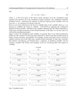
(a) (b)
Fig. 2. Spectra of imidazolium undecachlorodibismuthate (III) converted on single phonon
scattering approximation to the generalized density of vibrational states G(υ) (Holderna-
Natkaniec, 2006).
Low frequency region of generalized density of state at 20 K(fig.2a) and 294 K (fig.2b).
Ferroelectrics - Characterization and Modeling
46
4. Discussion
Calculations of the vibrational spectra require the molecular structure and the force field
constants to be known
. In order to analyse the low-temperature spectrum of ICB the
structures of isolated molecule of diamagnetic Im, (Im)
+
, Im
+
Cl
-
system and the
connection of imidazolium cations with the halogenobismuthate(III) anion were
optimised. The force field was determined as a derivative of the total energy of the
molecule over the atoms’ displacements. Fig. 3 presents the structure of an isolated
imidazolium cation and the notation assumed. Table 1 collects the bond lengths and
angles between the bonds determined on the basis of X-ray diffraction at 150 K by S.
Martinez-Carrera, (1966) and from the neutron diffraction data by B.M. Craven, R.K.
McMullan, J.D. Bell, H.C. Freeman, (Craven et al., 1977) given at 150 K for imidazole
(
abbreviation Im) and for the sample of ICB studied at room temperature (Jakubas, 2005)
together with the structure optimisation data (Holderna-Natkaniec,2006). On the basis of
the X-ray and neutron diffraction data (Piecha et al., 2007; Zhang et al., 2005; Adams et
al.,2008; Levasseur et.al., 1991; Zhang et al., 2005; Valle&Ettorare ,1997) it can be
concluded that imidazolium cation actually does not have the mm2 symmetry. However,
the five-membered ring of imidazole skeleton is planar, but the hydrogen atoms lay more
than 0.16 Å out-of-plane of the heterocyclic ring system, while both nitrogen atoms are
linked to hydrogen atoms. Similarly as the other heterocyclic ring systems, imidazole can
be represented as a resonance hybrid.
Fig. 3. Skeleton of imidazole with the atom numbering system.
The quality of the agreement of the experimental data X
exper
( Jakubas, 2005; Craven,1977)
with the values predicted by quantum mechanical calculations X
predicted
can be expressed by
the root mean square deviation determined as:
()
2
expcal
xx
RMS
n
−
=
. (2)
Internal Dynamics of the Ferroelectric (C
3
N
2
H
5
)
5
Bi
2
Cl
11
Studied by
1
H NMR and IINS Methods
47
Only the structure of the ordered (Im) skeleton (Jakubas, 2005) was used for comparison
with the other data collected in Table 1, as the hydrogen positions determined by X-Ray
diffraction are charged with too much error because of low electron density clouds of
hydrogen atom. The lowest RMS value for bond length and angles is 0.0011 Ǻ and 2.80
o
,
respectively. Consequently, the B3LYP/LanL2Dz method leads to the geometric parameters
of imidazole structure close to the experimental data.
Property
/bond
length
[A]
(Im)
5
Bi
2
Cl
11
X-ray [RT]
(Jakubas, 2005)
(Im)
o
B3LYP/
6-311G*
(Im)
+
B3LYP/
6-311G*
(Im)
+
LanL2Dz
(Im
+
)
3
BiCl
6
LanL2Dz
N1-C2
1.269
1.241 1.256 1.258 1.2156 1.349
3
1.2156 1.2156 1.2502 1.2158
C2-N3
1.216 1.265 1.276 1.333
1.2690 1.326
3
1.2590 1.2690 1.2759 1.2650
N3-C4
1.352
1.365 1.329 1.368 1.3433 1.377
7
1.3432 1.3432 1.3290 1.3432
C4-C5
1.241
1.328 1.298 1.238 1.2413 1.358
0
1.2413 1.2412 1.2977 1.2412
C5-N1
1.343
1.374 1.338 1.354 1.3525 1.369
0
1.3524 1.3524 1.3380 1.3526
N1-H
N2-H
0.819
1.153
1.044
1.052
1.017
1.172
0.840
1.0715
1.047
0
0.999
9
1.0000
1.0000
1.000
1.000
1.000
1.000
1.000
1.000
C2-H 1.108 1.118 1.078 0.866 1.1091 1.0822 1.0900 1.091 1.090 1.0899
C4-H 1.033 1.020 1.119 0.851 1.0933 0.9583 1.0900 1.090 1.0899 1.0900
C5-H 1.003 0.946 0.957 1.046 1.0334 1.0307 1.009 1.0899 1.090 1.0900
Angles
[deg]
C5 N1
C2
107.5
9
110.03 108.04 111.95 108.59 107.26 108.59 108.59 108.04 109.59
N1 C2
N3
109.41
106.31 110.00 103.05 109.50 111.26 109.40 109.40 110.99 109.40
C2 N3
C4
107.80
97.69 106.76 111.17 107.79 105.38 107.79 107.79 106.75 107.79
N3 C4
C5
106.64
100.36 107.37 104.74 106.55 109.77 106.53 106.53 107.87 106.54
C4 C5
N1
107.37
108.35 106.93 109.03 107.37 109.77 107.37 107.37 106.33 107.37
C5 N1 H
119.60
125.3 121.22 116.10 122.44 133.31 125.70 125.97 125.70
N1 C2 H
121.02
122.15 116.29 115.29 125.72 110.44 125.29 124.50 125.29
C5 C4 H
128.94
120.36 141.30 147.02 131.97 133.21 126.73 107.87 126.73
N1 C5 H 122.90 121.39 120.05 110.30 128.25 117.38 126.31 126.83 126.31
RMS (l) 0.0011 0.0067 0.0009 0.0011 0.0015 0.0015
RMS(∠)
2.75 6.44 2.84 2.85 2.84
Table 1. Comparison of observed and calculated geometry of imidazole. (in bold - the
parameters of ordered structure).
Fig.4 presents the low-temperature spectra of the phonon density of states G
exp
(ν) for ICB
compared with the spectra calculated by DFT and semi-empirical methods for the systems
discussed, in the energy transfer range up to 1700 cm
-1
. Harmonic vibrational wavenumbers
of normal modes computed for the reference systems and those corresponding to the
experimental of ICB are listed in Table 2. It can be seen that the agreement is remarkable,
showing that the DFT/LanL2Dz performed for a simple system built of imidazolium cation
and BiCl
6
anion has accurately modelled the system, while the region of internal modes is
well described by DFT/B3LYP/6-311G** performed for isolated imidazolium cation. The
frequencies are unscaled.
As shown Fig.4, the internal vibration of anion mainly influence the phonon density of state
spectrum in the lattice branch region (below 400 cm
-1
).
Ferroelectrics - Characterization and Modeling
48
Fig. 4. Comparison of the low temperature phonon density of state spectra of imidazolium
undecachlorodibismuthate (III) (C) with the ones calculated in the isolated molecule
approximation by the Density Functional Theory method B3LYP with 6-311G** and
LanL2Dz basis sets for the following systems: (Im) (A) , (Im)
+
(B), (Im)
3
BiCl
6
(D),
respectively (below energy transfer 800 cm
-1
in Holderna-Natkaniec, 2008).