Ferroelectrics Characterization and Modeling Part 4 ppt
Bạn đang xem bản rút gọn của tài liệu. Xem và tải ngay bản đầy đủ của tài liệu tại đây (6.43 MB, 35 trang )
Impact of Defect Structure on ’Bulk’ and Nano-Scale Ferroelectrics 17
Banys (University of Vilnius). Financially, this research has been supported by the DFG center
of excellence 595.
7. References
[1] Scott, J. F. (2000). Ferroelectric Memories, Springer, Berlin.
[2] Was er, R. (2005). Nanoelectronics and Information Technology, Wiley.
[3] Setter, N. (2002). Piezoelectric Materials in Devices, Swiss Federal Institute of Technology,
Lausanne.
[4] Smyth, D. M. ( 2000). The Defect Chemistry of Metal Oxides, Oxford University Press, New
York.
[5] Eichel, R A. (2008). J. Am. Ceram. Soc., Vol. 91, 691.
[6] Morozov, M.I.; Damjanovic, D. (2010). J. Appl. Phys., Vol. 107, 034106.
[7] Rüdiger, A.; Schneller, T.; Roelofs, A.; Tiedke, S.; Schmitz, T.; Waser, R. (2005). A ppl.
Phys. A, Vol. 80, 1247.
[8] Böttcher, R.; Klimm, C.; Michel, D.; Semmelhack, H. C.; Völkel, G.; Gläsel, H. J.;
Hartmann, E. (2000). Phys.Rev.B, Vol. 62, 2085.
[9] Eichel, R A.; Erünal, E,; Drahus, M.D.; Smyth, D.M.; van Tol, J.; Acker, J.; Kungl, H.;
Hoffmann, M.J. (2009). Phys. C hem. Chem. Phys., Vol. 11, 8698.
[10] Erünal, E.; Eichel, R A.; Körbel, S.; Elsässer, C.; Acker, J.; Kungl, H.; Hoffmann, M.J.
(2010). Funct. Mat. Lett. Vol. 3, 19.
[11] Hu, Y. M .; Gu, H. S.; Chen, W. P.; Wang Y. (2010). Mater. Chem. Phys., Vol. 121, 10.
[12] Fukui, T. (1998). J. Sol-Gel Sci. Tech., Vol. 11, 31.
[13] Zorel, H. E.; Ribeiro, C. A.; Crespi, M. S. (2001). J. Mater. Sci. Lett., Vol. 20, 621.
[14] Selbach, S. M.; Wang, G.; Einarsrud,M A.; Grande, T. (2007). J. Amer. Cer. Soc., Vol. 90,
2649.
[15] Erdem, E; Böttcher, R.; Semmelhack, H C.; Gläsel, H J.; Hartmann, E.; Hirsch, D.
(2003). J. Mater. Sci., Vol. 38, 3211.
[16] Erdem, E; Kiraz, K.; Somer, M.; Eichel, R A. (2010). J. Eur. Ceram. Soc., Vol. 30, 289.
[17] Parashar, S. K. S.; Choudhary, R. N. P.; Murty, B. S. (2003). J. Appl. Phys., Vol. 94, 6091.
[18] Parashar, S. K. S.; Choudhary, R. N. P.; Murty, B. S. (2004). Mat. Sci. Eng. B, Vol. 110, 58.
[19] Gläsel, H. J.; Hartmann, E.; Hirsch, D.; Böttcher, R.; Klimm, C.; Michel, D.; Semmelhack,
H. C.; Hormes, J.; Rumpf, H. (1999). J. Mater. Sci., Vol. 34, 2319.
[20] Lines, M. E.; Glas, A. M. (2001). Principles and Applications of Ferroelectrics and Related
Materials, Oxford, Great Britain.
[21] Xu, Y. (1991). Ferroelectric Materials and Their Applications, North Holland, Amsterdam.
[22] Strukov, B. A.; Levanyuk, A. P. (1998). Ferroelectric Phenomena in Crystals: Physical
Foundations, Springer, Berlin.
[23] Kretschmer, R.; B inder, K. (1979). Phys. Rev. B, Vol. 20, 1065.
[24] Tilley, D. R.; Zeks, B. (1984). Sol. Stat. Commun., Vol. 49, 823.
[25] Glinchuk, M. D.; Eliseev, E. A.; Stephanovich, V. A. (2002). Physica B-Condens. Matter,
Vol. 322, 356.
[26] Zhong, W. L.; Wang, Y. G.; Zhang, P. L.; Qu, B. D. (1994). Phys. Rev. B, Vol. 50, 698.
[27] Wang, C. L.; Smith, S. R. P. (1995). J. Phys. Condens. Matter, Vol. 7, 7163.
[28] Rychetsky, I; Hudak, O (1997). J. Phys. Condens. Matter, Vol. 9, 4955.
[29] Sheshadri, K.; Lahiri, R.; Ayyub, P.; Bhattacharya, S. (1999).
J. Phys. Condens. Matter,Vol.
11, 2459.
[30] Glinchuk, M. D.; M orozovskaya, A. N . (2003). phys. statu. solidi B, Vol. 238, 81.
[31] Glinchuk, M. D.; Bykov, P. I. (2004). J. Phys. Condens. Matter, Vol. 16, 6779.
95
Impact of Defect Structure on ’Bulk’ and Nano-Scale Ferroelectrics
18 Ferroelectrics
[32] Devonshire, A . F. (1949). Philosophical M agazine, Vol. 40, 1040.
[33] Ishikawa, K .; Yoshikawa, K.; Okada, N. (1988). Phys. Rev. B, Vol. 37, 5852.
[34] Shih, W. Y.; Shih, W. H.; Aksay, I. A. (1994). Phys. Rev. B, Vol. 50, 15575.
[35] Morozovska, A. N.; Glinchuk, M. D; Eliseev, E. A . (2007). Phys. Rev. B, Vol. 76, 014102.
[36] Burns, G.; Scott, B. A. (1973). Phys. Rev. B, Vol. 7, 3088.
[37] Mesquita, A.; Michalowicz, A.; Mastelaro, V. R. (2009). Journal of Physics: Conference
Series, Vol. 190, 012081.
[38] Vedrinskii, R. V.; Kraizman, V. L.; N ovakovich, A. A.; Demekhin, P. V.; Urazhdin, S. V.
(1998). J. Phys. Condens. Mat. Vol. 10, 9561.
[39] Schneider, J. J.; Hoffmann, R. C.; Engstler, J.; Dilfer, S.; Klyszcz, A.; Erdem, E; Jakes, P.;
Eichel, R A. (2009). J. Mater. Chem., Vol. 19, 1449.
[40] Schneider, J. J.; Hoffmann, R. C.; Engstler, J.; Erdem, E; Jakes, P.; Eichel, R A.;
Bauermann, L P.; Bill, J. (2010). Chem. Mater., Vol. 22, 2203.
[41] Kröger, F.A.; Vink, H. J.(1956). In: Solid State Physics, Seitz, F.; Turnbull, D. (Ed.), Vol. 3,
273.
[42] Holman, R. L.; Fulrath, R. M. (1973). J. Appl. Phys., Vol. 44, 5227.
[43] Merkle, R.; Maier, J. (2003). Phys. Chem. Chem. Phys., Vol. 5, 2297.
[44] Kirkpatrick, E. S.; Müller, K. A.; Rubins, R. S. (1964). Phys. Rev., Vol. 135, A86.
[45] Waldkirch, T. von; Müller, K. A.; B erlinger, W. (1972). Phys. Rev. B, Vol. 5, 4324.
[46] Meštri´c, H.; Eichel, R A., Kloss, T.; Dinse, K P.; Laubach, So.; Laubach, St.; Schmidt,
P.C. (2005). Phys. Rev. B, Vol. 71, 134109.
[47] Siegel, E.; Müller, K. A. (1979). Phys. R ev. B, Vol. 20, 3587.
[48] Possenriede, E.; Schirmer, O. F.; Donnerberg, H. J.; Godefroy, G.; Maillard, A. (1989).
Ferroelectrics, Vol. 92, 245.
[49] Kornienko, S.M.; Bykov, I. P.; Glinchuk, M. D.; Laguta, V. V.; Belous, A. G.; Yastrabik, L.
(1999). Phys. Solid State, Vol. 41, 1688.
[50] Böttcher, R.; Langhammer, H. T.; M üller, T.; Abicht, H. P. (2008). J. Phys. Condens. Matter,
Vol. 20, 505209.
[51] Eichel, R A.; Meštri´c,H.;Kungl,H.;Hoffmann,M.J.Appl. Phys. Lett., Vol. 92, 122506.
[52] Eichel, R A. (2007). J. Electroceramics, Vol. 19, 9.
[53] Erdem,E.;Eichel,R A.;Kungl,H.;Hoffmann,M.J.;Ozarowski,A.;vanTol,H.;Brunel,
L. C . (2007). Phys. Script., Vol. T129, 12.
[54] Meštri´c, H.; Eichel, R A.; Dinse, K P.; Ozarowski, A.; van Tol, J.; Brunel, L. C. (2004). J.
Appl. Phys., Vol. 96, 7440.
[55] Aoyagi, S.; Kuroiwa, Y.; Sawada, A. ; Kawaji, H. ; Atake, T. (1973). J. Thermal Analy. Calor.,
Vol. 81, 627.
[56] Erdem, E; Semmelhack, H C.; Böttcher, R.; Rumpf, H.; B anys, J.; Matthes, A.; Gläsel,
H J.; Hirsch, D.; Hartmann, E. (2006). J. Phys. C ondens. Matter, Vol. 18, 3861.
[57] Erdem, E.; Drahus, M. D.; Eichel, R A.; Kungl, H.; Hoffmann, M . J.; Ozarowski, A. ; van
Tol, H.; Brunel, L. C. (2008). Funct. Mat. Lett.,Vol.1,7.
[58] Guo, X.; Pithan, C.; Ohly, C.; Jia, C. L.; Dornseiffer, J.; Haegel, F. H.; Waser R. (2005).
Appl. Phys. Lett. Vol. 86, 082110.
96
Ferroelectrics - Characterization and Modeling
6
Microstructural Defects in
Ferroelectrics and Their Scientific Implications
Duo Liu
State Key Laboratory of Crystal Materials,
Shandong University, Jinan, Shandong,
P. R. China
1. Introduction
Properties of materials are closely linked to their defect structure. Numerous studies have
proved that the existence of a small amount of microstructural defects can dramatically
change the way of materials behaving in response to external fields. Based on these, various
kinds of functional devices have been developed, which have changed the daily life of
human beings. Currently, the most important application of defects in industry is probably
semiconductor devices intentionally doped with foreign atoms to realize desirable band
structures to tune the behaviors of electrons. Defects are also intentionally introduced into
metals and insulators to achieve better performances.
Similarly, defects in ferroelectric materials are also extremely important. As a subject that
has been investigated for decades, it has been proved that defects and the associated stress
and electrical fields could change ferroelectric behaviors such as polarization reversal,
domain kinetics, phase transition temperatures, and ferroelectric fatigue. Up to date,
numerous studies have been devoted to understanding oxygen vacancies, dislocations,
domain walls, voids, and microcracks in ferroelectrics. Actually, almost all aspects of
ferroelectric properties are defect-sensitive. For example, doped PZTs could either be “soft”
or “hard” with variable coercive fields. Oxygen vacancies play a determinant role on the
fatigue process of ferroelectric oxides. Dislocations may hinder the motion of ferroelectric
domain walls.
Recent interests on the design and fabrication of nanodevices stem from the distinct and
fascinating properties of nanostructured materials. Among those, ferroelectric
nanostructures are of particular interests due to their high sensitivity, coupled and ultrafast
responses to external inputs [1]. With the decrease of the size of ferroelectric component
down to nanoscale, a major topic in modern ferroelectrics is to understand the effects of
defects and their evolution [2]. Defects will change optical, mechanical, electrical and
electromechanical behaviors of ferroelectrics [3, 4]. However current understanding is
limited to bulk and thin film ferroelectrics and is still not sufficiently enough to describe
their behaviors at nanoscale. In view of the urgent requirement to integrate ferroelectric
components into microdevices and enhanced size-dependent piezoelectricity for nanosized
ferroelectric heterostructure, [5] it becomes essential to explore the role of defects in
nanoscale ferroelectrics.
Ferroelectrics - Characterization and Modeling
98
In this Chapter, the author will first discuss the effects associated with different types of
defects in BaTiO
3
, a model ferroelectric, from the point of views of the classical ferroelectric
Landau-Ginsberg-Devonshire (LGD) theory. The author will then present some recent
progresses made on this area. Among those include 1) critical size for dislocation in BaTiO
3
nanocube, 2) (111) twined BaTiO
3
microcrystallites and the photochromic effects.
2. Thermodynamic description of ferroelectrics
Most important phenomena associated with hysteretic, polarization, domain wall, and
phase transition behaviors in ferroelectrics can be described by using the thermodynamic
Landau-Ginzburg-Devonshire (LGD) theory. The LGD theory has been demonstrated to be
the most powerful tool to understand ferroelectric behaviors especially when the materials
are under the influence of external fields (electrical, temperature, and stress) [6, 7].
Most ferroelectric materials undergo a structural phase transition from a high temperature
non-ferroelectric paraelectric phase into a low temperature ferroelectric phase of a lower
crystal symmetry. The phase transition temperature is usually called the Curie temperature.
In most cases, the dielectric constant above the Curie temperature obeys the Curie-Weiss
law.
The change of internal energy, dU, of a ferroelectric material subjected to a small strain dx,
electric displacement dD
i
, and entropy dS can be expressed by
i
j
i
j
ii
dU TdS X dx E dD=+ + (1)
where T is the temperature of the thermodynamic system. Since most piezoelectric systems
are subjected to stress, electric field and temperature variations, it is convenient to express
the free energy into the form of the Gibbs energy
i
j
i
j
ii
dG SdT x dX D dE=− − −
(2)
According to the Taylor expansion around a certain equilibrium state,
G
0
(T), the Gibbs free
energy can be expanded in terms of the independent variables T, X and D
2
2
0
2
222
22
1
()
2
111
222
11
22
ij i
ij i
i
j
kl i
j
i
j
ij kl i j ij
jijk
jiik
GGG G
GGT T X D T
TX D
T
GGG
XX DD TX
XX DD TX
GG
TD X D
TD X D
∂∂∂ ∂
=+Δ+ + + Δ
∂∂ ∂
∂
∂∂∂
+++Δ
∂∂ ∂∂ ∂∂
∂∂
+Δ+ +⋅
∂∂ ∂ ∂
⋅⋅⋅⋅⋅
(3)
This phenomenological theory treats the material in question as a continuum without regard
to local microstructure variations [8]. Although the treatment itself does not provide
physical insight on the origin of ferroelectricity, it has been demonstrated as the most
powerful tool for the explanation of some ferroelectric phenomena such as Curie-Weiss
relation, the order of phase transition and abnormal electromechanical behaviors [9].
Equation (3) can be rewritten as [10]:
Microstructural Defects in Ferroelectrics and Their Scientific Implications
99
222 444 222322
1123 11123 12122313
666 422 422 422
111 1 2 3 112 1 2 3 2 1 3 3 2 1
222 2 2 2
123 1 2 3 11 1 2 3 12 1 2 2 3 1 3
222
44 4 5 6 11
()()( )
()[()()()]
1
()( )
2
1
()
2
GaPPP aPPP aPPPPPP
aPPP aPPP PPP PPP
aPPP sXXX sXXXXXX
sXXX Q
Δ= + + + + + + + +
++++ +++++
+−++−++
−++−
222
11 22 33
22 22 22
12 1 2 3 2 1 3 3 2 1
44 423 423 621
()
[( ) ( ) ( )]
()
XP XP XP
QXPP XPP XPP
QXPPXPPXPP
++
−+++++
−++
(4)
where the coefficients, α
1
, α
2
, and α
3
can be identified from equation (4) and s and Q are
known as the elastic compliance and the electrostrictive coefficient, respectively.
For a ferroelectric perovskite, equation (4) can be further simplified if the crystal structure
and the corresponding polarization are taken into consideration. The polarization for cubic,
tetragonal, orthorhombic and rhombohedral ferroelectrics is listed in Table 1, where 1, 2,
and 3 denotes the a-, b-, and c- axis in a unit cell.
Cubic
222
123
0PPP===
Tetragonal
22
12
0PP==,
2
3
0P ≠
Orthorhombic
22
12
0PP=≠,
2
3
0P =
Rhombohedral
222
123
0PPP==≠
Table 1. The polarization for cubic, tetragonal, orthorhombic, and rhombohedral structures.
Thus, considering the tetragonal ferroelectric system in the absence of external electrical field
and without temperature change, the electric displacement, D, equals to the polarization in the
direction parallel to the c- axis. The free energy can then be further simplified as
()
24622
0123
1111
2462
GGT aP aP aP sX QXP= + + + + + +⋅⋅⋅⋅⋅⋅
(5)
where a
1
=β (T - T
c
) with β a positive constant, T
c
is the Curie temperature for second-order
phase transitions or the Curie-Weiss temperature (≠ the Curie temperature) for first-order
phase transition.
3. Point defects
Point defects occur in crystal lattice where an atom is missing or replaced by an foreign
atom. Point defects include vacancies, self-interstitial atoms, impurity atoms, substitutional
atoms. It has been long realized even the concentration of point defects in solid is considered
to be very low, they can still have dramatic influence on materials properties [11,12]:
•
Vacancies and interstitial atoms will alternate the transportation of electrons and atoms
within the lattice.
•
Point defects create defect levels within the band gap, resulting in different optical
properties. Typical examples include F centers in ionic crystals such as NaCl and CaF
2
.
Crystals with F centers may exhibit different colors due to enhanced absorption at
visible range (400 – 700 nm).
Ferroelectrics - Characterization and Modeling
100
The most important point defect in ferroelectric perovskites is oxygen vacancies. Perovskite-
related structures exhibit a large diversity in properties ranging from insulating to metallic
to superconductivity, magneto-resistivity, ferroelectricity, and ionic conductivity. Owing to
this wide range of properties, these oxides are used in a great variety of applications. For
example, (Ba,Sr)TiO
3
and Pb(Zr,Ti)O
3
are high-dielectric constant materials being
considered for dynamic and nonvolatile random access memories, Pb(Zr,Ti)O
3
is high
piezoelectric constant material being used for actuators and transducers, and LaMnO
3
and
(La,Sr)CoO
3
are being used as electrode materials in solid oxide fuel cells. Oxygen vacancies
in perovskites are particularly of interests due partly to the loosely packed oxygen octahedra
that lead to high mobility of oxygen vacancies. In perovskite ferroelectrics, a lot of works
have been conducted to understand the behaviors of oxygen vacancies under the influence
of external fields, such as electrical, stress and thermal fields, sometimes as a function of
temperatures [13]. Oxygen vacancies play an essential role on ferroelectric fatigue during
the operation of a ferroelectric component subjected to continuous load of electrical or stress
fields, though many other factors such as microcracks [14], spatial charges [21],
electrodes[15], surfaces and interfaces[16], voids, grain boundaries [21] may also lead to
ferroelectric fatigue. The accumulation of oxygen vacancies in the electrode/ferroelectric
interface has been confirmed by experimental studies. This oxygen deficient interface region
could either screen external electrical field [24,17] or pin domain walls [18], both of which
will reduce the polarizability of the ferroelectric thin films. Although ferroelectric fatigue
induced by the accumulation of oxygen vacancies is considered to be permanent, thermal or
UV treatment in oxygen rich environment can sometimes partially recover the switchability.
Another option is to use conductive oxide electrode materials such as LSCO or YBCO which
can serve as sinks for oxygen vacancies and prevent their accumulation at the electrode/film
interface [19,20].
Recently, efforts have been made on hydrothermal synthesis of BaTiO
3
nanoparticles of
various sizes to understand the ferroelectric size effect by using BaCl
2
and TiO
2
as the
starting materials.
[21,22]. The growth of BaTiO
3
nanoparticles is commonly believed to
follow a two step reaction mechanism: 1) the formation of Ti-O matrix, 2) the diffusive
incorporation of Ba
2+
cations. The second step is believed to the rate determinant process.
Due to the presence of H
2
O, OH
-
groups are always present in hydrothermal BaTiO
3
. As a
result, some studies have been performed to understand OH- effects on ferroelectricity. D.
Hennings et al reported that a reduction of hydroxyl groups in BaTiO
3
nanoparticles
promotes cubic-to-tetragonal phase transition [23]. Similar results had also been obtained
by other studies on BaTiO
3
particles with sizes varying from 20 nm to 100 nm [24,25].
These experimental observations imply that point defects and possibly the associated
electrical fields can lead to structural phase transition, as suggested by the soft-mode
theory.
Currently, point defects in ferroelectrics are mostly studied by optical methods such as FT-
IR spectroscopy or Raman spectroscopy. For BaTiO
3
, the stretching vibration of lattice OH-
groups occurs at 3462.5-3509.5cm
-1
, characterized by a sharp absorption peak [26]. In
contrast, surface OH- groups are characterized by a broad absorption peak located at 3000-
3600 cm
-1
[44,27] due to the uncertain chemical environment on surface region. Raman
spectroscopy is also a powerful tool to understand the size effect of ferroelectrics, which is
quite sensitive to local variation of lattice structure. S. Wada et al. reported that OH- groups
in BaTiO
3
correspond to an 810 cm
-1
Raman shift [28]. As point defects can create extra
Microstructural Defects in Ferroelectrics and Their Scientific Implications
101
electron levels in the band gap, photoluminescent spectroscopy had also been utilized to
study the band structure of BaTiO
3
, which is frequently conducted at low temperatures.
Some other techniques such as HRTEM [29] and AFM [30] have also been used to study
point defects.
4. Dislocations in ferroelectrics
The LGD theory predicts that dislocations in a ferroelectric will change the local ferroelectric
behaviors around them. Considering a perovskite ferroelectric single domain with a
tetragonal structure, the coordinate system is defined as x//[100], y//[010], and z//[001]
with the spontaneous polarization, P
3
, parallel to the z axis and P
1
=P
2
=0. The variation of
piezoelectric coefficients induced by a {100} edge dislocation can be found with a method
derived from combination of the Landau-Devonshire free energy equation [10] and
dislocation theory [31]. As previous works suggest [32], the elastic Gibbs free energy around
an edge dislocation can be modified as
24 6 22
0 1 11 111 11 11 22
22
33 12 11 22 11 33 22 33 44 12
1
[,, (,)] (
2
1
)( )
2
ij
core
GPT xy G aP a P a P s
ssE
σσσ
σσσσσσσ σ
∗
=+ + + + +
+++++
(6)
with
*
1 1 11 33 12 11 22
[ , ( , )] [ ( )]
ij
aT xy a Q Q
σσσσ
=− + + (7)
where G
0
is the free energy in the paraelectric state, a
1
, a
11
and a
111
are the dielectric stiffness
constants at constant stress,
i
j
σ
is the internal stress field generated by an edge dislocation, P
is the spontaneous polarization parallel to the polar axis, s
ij
is the elastic compliance at
constant polarization, E
core
is the dislocation core energy and Q
ij
represents the
electrostriction coefficients. The stress field generated by an edge dislocation is well
documented in the literature and is known as
22
11
222
(3 )
2(1 )
()
y
x
y
b
xy
μ
σ
πν
+
=−
−
+
,
22
22
222
()
2(1 )
()
y
x
y
b
xy
μ
σ
πν
−
=
−
+
33 11 22
()
σνσσ
=+
,
22
12
222
()
2(1 )
()
xx
y
b
xy
μ
σ
πν
−
=
−
+
(8)
13 23
0
σσ
==
where
μ
is the shear modulus, b is the Burgers vector and
ν
is Poisson’s ratio. A schematic
plot of the stress field surrounding an edge dislocation is given in Fig. 1a.
The variation of the spontaneous polarization associated with the stress field due to an edge
dislocation is then found by minimizing the modified Landau-Devonshire equation with
respect to polarization
()
0
G
P
∂
=
∂
. Upon rearrangement, this gives [7]
Ferroelectrics - Characterization and Modeling
102
2*
11 11 1 111
2
111
(3[,(,)])
[, (,)]
3
ij
ij
aaaTxya
PT xy
a
σ
σ
−+ −
=
(9)
Once the polarization is known for a given position, the piezoelectric coefficient, d
33
, can be
calculated by using [2]
33 33 11
2dQP
ε
=
(10)
where d
33
is the piezoelectric coefficient along the polar axis.
Elastic Constants Piezoelectric Coefficients
11
C (GPa)
275 T (K) 298
12
C (GPa)
179
()
1
1
aVmC
−
5
3.34 10 ( 381)T×−
13
C (GPa)
152
()
53
11
aVmC
−
()
68
4.69 10 393 2.02 10T×−−×
33
C (GPa)
165
()
95
111
aVmC
−
()
79
5.52 10 393 2.76 10T−× − + ×
44
C (GPa)
54
()
42
11
QmC
−
0.11
66
C (GPa)
113
()
42
12
QmC
−
0.045−
Table 2. Elastic and piezoelectric properties required for theoretical calculations for barium
titanate single crystals.
The elastic compliance, dielectric stiffness constants and electrostriction coefficients used in
the calculation were found for BaTiO
3
from other works [33,34]. The resulting d
33
contour
around the dislocation core is plotted and shown in Fig. 1b, where some singular points
resulted from the infinite stress at the dislocation core are discarded. It is clearly seen that
the piezoelectric coefficient d
33
deviate from the standard value (86.2 pm/V at 293 K), due to
the presence of the stress field. The area dominated by transverse compressive stresses
exhibits an enhanced piezoelectric response while the area dominated by tensile stresses
shows reduced effects. Note that the influence of stress field shows asymmetric effects on
the piezoelectric coefficients due to the combination of equations (7) and (9). This simple
calculation also suggests that the area significantly influenced by an edge dislocation could
easily reach tens of nanometers as a result of the dislocation long-range stress field. In
addition, dislocation stress field will also change the local properties of its surrounding area,
like chemical reactivity, electron band structure, absorption of molecules and so on.
However, stress field solely sometimes is not sufficient to describe all effects; a fully
understanding of dislocation effects on ferroelectricity requires in-depth knowledge on
electrical fields induced by the charged core area, which is currently not fully addressed in
literature.
Microstructural Defects in Ferroelectrics and Their Scientific Implications
103
┴┴
86.202
86.097
86.022
85.947
82
89
d
33
(pm/V)
85.872
86.547
86.472
86.397
86.322
-250 -125
0
125 250 (nm)
┴
86.202
86.097
86.022
85.947
82
89
d
33
(pm/V)
85.872
86.547
86.472
86.397
86.322
-250 -125
0
125 250 (nm)
86.202
86.097
86.022
85.947
82
89
d
33
(pm/V)
85.872
86.547
86.472
86.397
86.322
-250 -125
0
125 250 (nm)
┴
(a) (b)
Fig. 1. The schematic representation of the stress field around an edge dislocation (a) and the
resulting piezoelectric coefficient contour (b) calculated from the Landau-Devenshire theory.
Recently, many studies have been performed to understand dislocation effects on
ferroelectricity. M. W. Chu et al. [35] found that misfit dislocations between PZT islands and
SrTiO
3
substrate (height: 4nm, width: 8 nm) can lead to polarization instability, as confirmed
by HRTEM and PFM tests. C. L. Jia et al [36] found that the elastic stress field of a
dislocation in SrTiO
3
/PZT/SrTiO
3
multilayered structures, even if it is located in regions far
from the ferroelectric material, can have a determinant effect on ferroelectricity. A decrease
of local spontaneous polarization of 48% was obtained by calculation. C. M. Landis et al.
[37] found by non-linear finite element method (FEM) simulation that the stress field of
dislocations can pin domain wall motions. L. Q. Chen et al [38] found by phase field
simulations that misfit dislocations will alternate ferroelectric hysteresis. D. Liu et al
performed nano indentation tests on individual 90
o
and 180
o
domains on BaTiO
3
single
crystal and found that in an area free of dislocations the nucleation of dislocations induced
by an indenter with tip radius of several tens of nanometers will be accompanied by the
formation of ferroelectric domains of complex domain patterns, as confirmed by PFM tests.
Recently, dislocation effects had been extended to other areas. For example, a theoretical
work even predicted that dislocations may induce multiferroic behaviors in ordinary
ferroelectrics [39]. In a recent study, the Author’s group found that there exists a critical size
below which dislocations in barium titanate (BaTiO
3
), a model ferroelectric, nanocubes can
not exist. While studying the etching behaviors of BaTiO
3
nanocubes with a narrow size
distribution by hydrothermal method, it was confirmed that the etching behaviors of BaTiO
3
nanocubes are size dependent; that is, larger nanocubes are more likely to be etched with
nanosized cavities formed on their habit facets. In contrast, smaller nanocubes undergo the
conventional Ostwald dissolution process. A dislocation assisted etching mechanism is
proposed to account for this interesting observation. This finding is in agreement with the
classical description of dislocations in nanoscale, as described theoretically [40].
5. Dislocation size effect
The author’s group reported an interesting observation on BaTiO3 nanocubes synthesized
through a modified hydrothermal method. Detailed analysis is provided as follows. The
Ferroelectrics - Characterization and Modeling
104
experimental procedure is relatively simple. First a small amount of NaOH:KOH mixture
was placed into a Teflon-lined autoclave. After the addition of BaCl
2
and TiO
2
(anatase), the
autoclave was sealed and heated at 200
o
C for 48 hours. After reaction, the product was
collected by filtering and washing thoroughly with deionized water and diluted HCl acid.
The reaction is as follows:
2NaOH + TiO
2
+ BaCl
2
→ BaTiO
3
+ 2NaCl + H
2
O (11)
The free Gibbs energy of the formation of BaTiO
3
at 200°C was calculated. The enthalpy of
formation is
ΔH = 2ΔH
NaCl
+ ΔH
H2O
+ ΔH
BaTiO3
- (2ΔH
NaOH
+ ΔH
BaCl2
+ ΔH
TiO2
)
= -2
×411.2 – 285.830 – 1659.8 – ( - 2×425.6–855.0 – 944.0) = -117.83 KJ·mol
-1
The entropy of formation is
ΔS = 2S
NaCl
+ S
H2O
+ S
BaTiO3
- (2S
NaOH
+ ΔS
BaCl2
+ S
TiO2
)
= 2
×72.1 + 69.95 + 108.0 – (2 × 64.4 + 123.67 + 50.62) = 19.06 J
o
C·mol
-1
Then the free Gibbs energy of formation at reaction temperature 200
o
C is
ΔG = ΔH-T ΔS
= - 117.83 – 19.06
×473/1000 = -126.845 KJ·mol
-1
It can be seen that the formation of BaTiO
3
proceed easily at 200
o
C. Our experiments had
shown that BaTiO
3
nanocubes can be formed at temperatures as low as 180°C, as shown in
Fig. 2, much lower than the temperature required by conventional solid-state reactions. All
the diffraction peaks can be indexed to tetragonal BaTiO
3
(P4mm, JCPD 81-2203).
Fig. 2. XRD patterns of BaTiO
3
nanocubes synthesized at a) 180
o
C , b) 200
o
C and c) 220
o
C.
Microstructural Defects in Ferroelectrics and Their Scientific Implications
105
After the synthesis of BaTiO
3
nanocubes, we also studied their etching behaviors in
hydrothermal environment. The etching process of BaTiO
3
nanocubes was carried out in
diluted HCl solution (1M). The BaTiO
3
nanocubes were first mixed with HCl solution and
then the mixture was treated in hydrothermal environment at 120
o
C for 2.5 hours. The
reaction time and temperature had been optimized in consideration that over reaction may
lead to the formation of TiO
2
, as shown in Fig. 3 and Fig. 4.
Fig. 3. XRD patterns of the final products after hydrothermal treatment at 120
o
C for various
time: a) 30 min, b) 40 min, c) 50 min, d) 60 min. The ▼ and ● marks correspond to rutile and
anatase TiO
2
, respecitively.
Fig. 4. SEM images of the final products after hydrothermal treatment at 120
o
C for a) 30 min,
b) 40 min, c) 50 min, and d) 60 min.
Ferroelectrics - Characterization and Modeling
106
Fig. 5a shows a typical SEM image obtained on the as-synthesized product. It can be seen
that all nanoparticles exhibit a cubic morphology with sizes of ~ 30-100 nm. FTIR analysis
reveals that the BaTiO
3
nanocubes contain a very small amount of lattice OH- groups,
considerably less than BaTiO
3
nanoparticles synthesized by regular hydrothermal method.
Fig. 5b shows a typical SEM image of the etched product, which reveals particle sizes
smaller than that of the as-synthesized product (Fig. 5a). Besides, it is also interesting to note
the fact that small cavities are formed on some nanocubes.
200 nm
200 nm
(a) (b)
Fig. 5. SEM image of BaTiO3 nanocubes before (a) and after (b) hydrothermal etching.
(Copyright 2008 @ American Chemical Society.)
A statistical analysis reveals that these cavities only present on nanocubes greater than ~60
nm. Fig. 5 shows SEM images of nanocubes of different sizes obtained under the same
experimental conditions. It can be clearly seen that nanocubes smaller than ~60 nm remain
intact, while cavities are selectively formed on those greater than ~60 nm. The etching
process was initiated on the surface and can penetrate all the way through a nanocube. In
most case, there is only one etch pit in one nanocube while occasionally there are two or
three etch pits observed.
Fig. 6. SEM images of BaTiO
3
nanocubes after hydrothermal etching.
Microstructural Defects in Ferroelectrics and Their Scientific Implications
107
All the observation seems to be in controversy to the Ostwald dissolution mechanism, which
predicts that small particles will dissolve first during a chemical reaction. However, our
experiments reveal that smaller BaTiO
3
nanocubes show a better chance to remain intact
though their corners and edges seem to have dissolved. The dissolution of corners and
edges could be understood based on the Gibbs-Thompson relation. The Gibbs-Thompson
relation suggests that, for a small particle, its corners and edges have enhanced chemical
reactivity and their dissolutions are energetically favored. The Gibbs-Thompson relation
also implies that smaller nanocubes have higher dissolubility and should dissolve first in
compensation of the growth of larger ones.
Fig. 7a shows a typical HRTEM image taken on a BaTiO
3
nanocube with length of ~ 15 nm.
It is evident that the nanocube is enclosed by (100) and (110) habit facets due to their high
chemical stabilities [41]. Fig. 7b shows the fast Fourier transformation (FFT) image of Fig.
7a, which shows that the nanocube contains cubic lattices with lattice parameters of ~ 0.4
nm, suggesting that the nanocube is in cubic non-ferroelectric phase, in agreement with
many previous studies. A careful examination of the lattice on the enlarged FFT filter image
(Figure 7c) shows that the nanocube exhibit perfect lattice without dislocation or stacking
faults. However, on the surface region, defective layers with distinct structures were formed
due possibly to the presence of non-stoichiometric Ti-O layer as a result of Ba
2+
dissolution
in acid [42,43]. As suggested by previous studies, the formation of BaTiO
3
in base contains
two steps, namely the precipitation of Ti-O networks and the incorporation of Ba
2+
.
Similarly, the dissolution of BaTiO
3
in acid contains outward diffusion of Ba
2+
followed by
phase transition of Ti-O network into TiO
2
. As the Ti-O surface layers prevent Ba
2+
from
dissolution out of the Ti-O matrix, it can be expected that the dissolution rate of BaTiO
3
will
be slowed down as the reaction proceeds. It is also possible that at certain stage of the
reaction the particles may contain a BaTiO
3
core surrounded by a TiO
2
shell.
2 nm
(a)
(b)
(c)
Fig. 7. HRTEM image taken on a BaTiO3 nanocube (a), the corresponding FFT pattern (b),
and filtered image (c).
Ferroelectrics - Characterization and Modeling
108
In contrast, the existence of dislocation inside a nanoparticle will dramatically change the
way of the dissolution of nanoparticles. As dislocated regions are highly strained, regions
with dislocations usually exhibit enhanced chemical reactivity. Preferential removal of
atoms in the dislocation core area has been extensively observed on various materials such
as metals, semiconductors and insulators. Although point defects such as the
aforementioned oxygen vacancies and hydroxyl groups may also increase local etching rate,
unlike extended defects, their effect is limited in a very small region and, even if there is
any, should be observable on all nanocubes of various sizes no matter they are greater or
smaller than 60 nm.
This observation also implies that there exists a critical size for dislocation to present inside
BaTiO
3
nanocubes, and possibly all other nanoparticles. To understand this, we need to look
into more details about the elastic theory of dislocation in nanoparticles. A literature review
reveals that the classical elastic theory indeed predicts a characteristic length below which
dislocation can not exist within an isolated nanoparticle [44, 45]. It was suggested that
dislocations would be driven out of the crystal spontaneously when the size of the crystal is
less than a characteristic length given by [46,47]
2
c
p
Gb
A
σ
≅ (12)
where G is the shear modulus, b is the Burgers vector of the dislocation, and σ
p
is the Peierls
stress given by [48]
2
max
33(1 )
2
p
a
Gb
υ
στ
−
= (13)
where G is the shear modulus of the material, a the lattice parameter, υ the Poisson’s ratio,
and τ
max
the ideal shear strength.
For BaTiO
3
, the average shear modulus is estimated to be 55 GPa with a method introduced
by Watt and Peselnick [49], Burgers vector b = a[110]/2=0.28 nm, and the ideal shear
strength of 5.5 GPa, as determined by nanoindentation test [50]. Bu substituting the data
into equation (13), A
c
for spherical BaTiO
3
nanoparticles is estimated to be ~22 nm. The
calculated value is smaller than that determined experimentally due to a combination of the
following factors: (1) the assumption of spherical shape used in the original model may not
be fully transferrable to cubic shaped nanoparticles; (2) the elastic anisotropy of BaTiO
3
means that an average shear modulus may not be sufficiently accurate; (3) the presence of
the Ti-O surface layers may also lead to alternate the case from the model; (4) possibly the
most important, ferroelectric size effects could also play a role. In fact, all these possibilities
lie on the fact that the elastic properties of BaTiO
3
nanocubes could deviate from the bulk
values. As a result, we performed first principle ab-initio calculation on BaTiO
3
with the
CASTEP module of Materials Studio in the assumption of the nanocubes having a cubic
lattice structure. The calculated elastic modulus are C
11
= 284.9 GPa, C
12
= 110.8 GPa, C
44
(shear modulus, G)= 116.2 GPa. The computed C
12
and C
44
agree well with experimental
values, while C
11
is ~10% greater than the experimental value [51]. Inserting C
44
to Equation
(13) yields a characteristic length of 46.5 nm, which is much closer to the observed critical
length. This calculation suggests that ferroelectric size effect has to be considered while
describing the etching behaviors of BaTiO
3
nanocubes. As discussed above, this critical size
Microstructural Defects in Ferroelectrics and Their Scientific Implications
109
effect is expected to be observed in other nanostructured materials. This had recently been
demonstrated in gallium nitride (GaN) [52].
6. (111) twins in BaTiO
3
The origin of ferroelectricity can be attributed to extrinsic contribution associated with
ferroelectric domain wall and intrinsic contribution from lattice distortion [10]. The extrinsic
contributions to ferroelectric properties are dominated by: (a) the population of domains,
and (b) the mobility of domain walls. In real ferroelectric materials, additional
considerations arise owing to the presence of the crystal surfaces and imperfections. In a
perfect crystal without imperfections or space charges, ρ is equal to zero. However, the free
charge density is different from the perfect crystal at the surface region or in the
neighborhood of defects, which alternatively results in the formation of a charge layer. This
charge layer may introduce a depolarization field in the nearby regions. When a ferroelectric
crystal is cooled from a paraelectric phase to a ferroelectric phase in the absence of applied
fields, different crystal regions may take one of these polarization directions such that the
total depolarization energy can be minimized. Each volume of uniform polarization is
referred to as a ferroelectric domain, and is bounded by domain walls are referred to as
domain walls.
There are two types of domain boundaries for a tetragonal perovskite, the polar axes of
which are perpendicular or antiparallel with respect to each other. The walls which separate
domains with oppositely orientated polarization are defined as 180
o
domain walls and those
which separate domains with perpendicular polarization are called 90
o
domain walls.
Unlike its ferromagnetic counterpart, a perovskite ferroelectric possesses a domain wall
width in the order of a few unit cells. Since the length of c- axis of a perovskite tetragonal
structure, c
T
, is slightly different from that of the a- axis, a
T
, the polarization vectors on each
side of a 90
o
domain wall form an angle slightly smaller than 90
o
. The angle can be
calculated by
1
2tan( / )
TT
ca
α
−
=× (14)
For BaTiO
3
, taking c
T
= 4.04 Å and a
T
= 3.99Å, one obtains 90.7
o
, as illustrated in Fig. 8.
Fig. 8. Schematic illustration of the 180° and 90° domain walls in BaTiO
3
.
Besides regular 90
o
and 180
o
twin walls, BaTiO
3
crystallites containing (111) twins have
also been reported. (111) twinned BaTiO
3
was first observed in single crystals grown via
0.7
o
0.7
o
[100]
(
1
1
0
)
Ferroelectrics - Characterization and Modeling
110
the Remeika method [53]
and in bulk ceramics [54] in 1950s. Existing evidences suggest
that the formation of (111) twins in ceramics are closely related to the exaggerated growth
of the hexagonal BaTiO
3
phases on the twin plane which involved oxygen octahedra
sharing the face [55]. It has also been suggested that (111) twins can lead to the
exaggerated growth of BaTiO
3
grains in ceramics following a twin-plane re-entrant edges
(TPREs) mechanism [56,57] since the decreasing of activation energy of nucleation on the
TPREs.
We recently reported the controlled synthesis of BaTiO
3
microcrystallites through a two-
step synthesis approach [58,59]. The synthesis method is quite similar to the synthesis of
BaTiO3 nanocubes, except that the starting anatase TiO
2
powders were first treated in
autoclave for 5 hours. Then, BaCl
2
and water were added into the autoclave, followed by
heat treatment at 180
o
C for different period of time up to 20 days. It is found that the
pretreated TiO
2
is essential for the synthesis of penetrated BaTiO
3
. The crystallites exhibit
penetrated morphologies and contain multiple (111) twins, originated from amorphous
TiO
2
clusters.
(a) (b)
(c)(d)
Fig. 9. SEM images of penetrated BaTiO
3
microcrystallite obtained at different synthesis
stages. (Copyright 2010 @ Royal Society of Chemistry).
Figure 10a shows the photograph of (111) twined BaTiO
3
nanoparticles before and after UV
irradiation. The UV-vis absorption spectra reveal the presence of defect energy levels after
UV irradiation. The color of the powders changes from pale yellow to dark brown after UV
irradiation. Oxygen vacancies create additional energy levels within the forbidden energy
gap of titanates,
usually 0.2-0.3 eV below the conduction band edge [60,61].Figure 10c shows
the XPS spectra of Ti-2p electrons before and after UV irradiation. A careful curve fitting
shows that a shoulder peak appears at position ~ 1.3 eV lower than that of Ti
4+
cations,
suggesting the presence of Ti
3+
cations [62]. The mechanism for the formation of Ti
3+
cations
is discussed as follows. As the valence band of BaTiO
3
is dominated by O-2p orbits, whereas
the conduction band is the Ti-3d orbits [17], electrons of O-2p orbits can be excited by UV
Microstructural Defects in Ferroelectrics and Their Scientific Implications
111
photons to the Ti-3d orbits, resulting in the formation of gaseous oxygen and leaving behind
oxygen vacancies inside the microcrystallites. The excited electrons are either trapped by
Ti
4+
to form Ti
3+
centers or are trapped by oxygen vacancies to form F-centers, both of which
could have strong absorption at visible region, resulting in the observed photochromic
effect. However, it is still unclear why the photochromic effect can hardly be observed on
regular BaTiO
3
nanocubes without (111) twins. It seems that the (111) twin walls may also
have a role during the process described above. Previous HRTEM investigations had
revealed that the (111) twin walls are composed of Ba-O
3-x
-[V
O
]
x
instead of Ba-O
3
plane to
balance the charge of adjacent Ti
4+
ions [63].
Fig. 11 shows the magnetization (M) versus applied magnetic field (H) curves measured
at room temperature before and after the UV irradiation. The green sample presents very
weak ferromagnetism with saturation magnetization of ~ 7×10
-5
emu/g. The saturation
magnetization for the UV irradiated BaTiO
3
crystallites is substantially enhanced and
becomes ~ 6.7×10
-4
emu/g, due to the increase of oxygen vacancies caused by UV
photons. However, the coercive field does not change and remains to be ~ 305 Oe. The
inset of Fig. 11 is the M-H curve of the sintered bulk sample. The sintered bulk sample is
diamagnetic. This behavior is similar to other nanosized oxides particles due to the
magnetic origin of defects.
466 464 462 460 458 456 454
0.0
5.0k
10.0k
15.0k
20.0k
25.0k
Counts / s
Binding Energy (eV)
Ti2p
3/2
Ti2p
1/2
BaTiO
3
Ti
3+
Green sample
0.0
5.0k
10.0k
15.0k
20.0k
25.0k
Ti2p
3/2
Ti2p
1/2
BaTiO
3
Ti
3+
UV irradiated sample
300 400 500 600 700 800
0.0
0.2
0.4
0.6
0.8
1.0
4 3.6 3.2 2.8 2.4 2 1.6
Abs. (a.u.)
Wavelength (nm)
Photon energy (eV)
UV irradiated sample
Green sample
300 400 500 600 700 800
0.0
0.2
0.4
0.6
0.8
1.0
4 3.6 3.2 2.8 2.4 2 1.6
Abs. (a.u.)
Wavelength (nm)
Photon energy (eV)
UV irradiated sample
Green sample
Green Sample
UV irradiated
(a)
(b)
(c)
Fig. 10. Photographs of (111) twinned BaTiO3 nanoparticles (a), the corresponding UV-vis
absorption spectra (b) and XPS spectra (c) before and after UV irradiation reveal
photochromic effect. (Copyright 2010 @ American Chemical Society).
Ferroelectrics - Characterization and Modeling
112
Fig. 11. Room-temperature M-H curves of the UV-irradiated BaTiO
3
sample and the as-
synthesized sample. The inset is the M-H curve of the sintered bulk sample. (Copyright 2010
@ American Chemical Society).
7. Conclusions
Insightful understanding and careful control of defect structures in ferroelectric does not
only provide an efficient tool for tuning ferroelectric properties, but also open a window for
exploring novel properties of ferroelectric materials, previously believed impossible or
negligible. We expect that there will be more investigations conducted on this area not only
from the viewpoint of ferroelectrics but also with cautious consideration of their technical
implications.
Acknowledgement. The authors would thank National Science Foundation of China
(NSFC) through grant # 50702031, # 51021062 and # 60974117, the Excellent Young
Investigators Award Foundation of Shandong Province (Grant No. BS2009CL021), SRF for
ROCS, State Education Ministry, National Basic Research Program of China (973 Program)
through grant # 2009CB930503) for financial support.
8. References
[1] Scott, J. F. Science. 2007, 315, 954-959.
[2] Damjanovic, D. Rep. Prog. Phys. 1998, 61, 1267-1324.
[3] Gopalan, V.; Dierolf, V. ; Scrymgeour, D. A.;Annu. Rev. Mater. Res., 2007
, 37, 449.
[4] Scrymgeour, D. A. ; Gopalan, V. ; Phys. Rev. B, 2005, 72, 24103.
[5] Majdoub, M. S; Sharma, P.; Cagin, T. Phys. Rev. B. 2008, 77, 125424-1-125424-9.
[6] Devonshire, A.F.; Philosophical Magazine, 1949, 40, 1040.
[7] Devonshire, A.F.; Philosophical Magazine, 1951
, 42, 1065.
[8] Lines M.E.; Glass, A.M.; Principles and applications of ferroelectrics and related materials
[Oxford University Press, New York, 1977].
[9] Abplanalp, M.; Fousek, J.; Gunter, P.; Phys. Rev. Lett., 2001
, 86, 5799.
[10] Haun, M.J.; Furman, E.; Jang, S.J.; Mckinstry, H.A.; Cross, L.E.; J. Appl. Phys., 1987
, 62, 3331.
Microstructural Defects in Ferroelectrics and Their Scientific Implications
113
[11] Agullo-Lopez, F.; Catlow, C. R. A.; Townsend, P.; Point Defects in Materials, 1988,
Academic Press, London.
[12] Stoneham, A. M. ; Theory of Defects in Solids, 1976, Clarendon Press, Oxford.
[13] Waser, R. ; Smyth, D. M.; Ferroelectric Thin Films: Synthesis and Basic Properties, ed. C. A.
P. Araujo, J. F. Scott, 1996, pp. 47–92, GW Taylor, Singapore: Gordon & Breach.
[14] Jiang, Q. Y. ; Subbarao, E. C ; Cross, L. E.; J. Appl. Phys., 1994, 75, 7433.
[15] Jiang, Q. Y. ; Subbarao, E. C. ; Cross, L. E. ; Ferroelectrics, 1994, 154, 119.
[16] Jiang, Q. Y. ; Cao, W. ; Cross, L. E. ; J. Am. Ceram. Soc., 1994, 77, 211.
[17] Duiker, H. M. ; Beale, P. D. ; Scott, J. F. ; Paz de Araujo, C. A. ; Melnick, B. M. ;
Cuchiaro, J. D. ; McMillan, L. D. ; J. Appl. Phys., 1990, 68, 5783.
[18] Scott, J. F. ; Dawber, M. ; Appl. Phys. Lett., 2000, 76, 3801.
[19] Ramesh, R. ; Gilchrist, H. ; Sands, T. ; Keramidas, V. G. ; Hakenaasen, R.; Appl. Phys.
Lett., 1993, 63, 3592.
[20] Ramesh, R. ; Lee, J. ; Sands, T. ; Keramidas, V. G. ; Auciello, O. ;Appl. Phys. Lett., 1994, 64,
2511.
[21] Chen, H. J. ; Chen, Y. W. ; Ind. Eng. Chem. Res., 2003, 42, 473.
[22] Dutta, P. K. ; Asiaie, R.; Akbar, S. A. ; Zhu, W. ; Chem. Mater., 1994, 6, 1542.
[23] Hennings, D.; Schreinemacher, S. ; J. Euro. Ceram. Soc., 1992, 9, 41.
[24] Wada, S. ; Suzuki, T. ; Noma, T. ;Jpn. J. Appl. Phys., 1995, 34, 5368.
[25] Wada, S. ; Suzuki, T. ; Noma, T. ; J. Ceram. Soc. Jpn., 1996, 104, 383.
[26] Kapphan, S.; Weber, G.; Ferroelectrics, 1981, 37, 673.
[27] Wada, S.; Suzuki, T. ; Noma, T. ; J. Ceram. Soc. Jpn., 1995, 103, 1220.
[28] Noma, T. ; Wada, S. ; Yano, M. ; Suzuki, T.; J. Appl. Phys., 1996, 80, 5223.
[29] Jia, C. L. ; Lentzen, M. ; Urban, K. ;Science, 2003, 299, 870.
[30] Namai, Y.; Matsuoka, O.; J. Phys. Chem. B, 2005, 109, 23948.
[31] Hirth J.P.; Lothe, J.; Theory of dislocations [Wiley, New York, ed. 2nd, 1982].
[32] Alpay, S.P.; Misirlioglu, I.B.; Nagarajan, V.; Ramesh, R.; Appl. Phys. Lett., 2004, 85, 2044.
[33] Berlincourt D.; Jaffe, H.; Phys. Rev., 1958
, 111, 143.
[34] Bell, A.J.; J. Appl. Phys., 2001, 89, 3907.
[35] Chu, M. W.; Szafraniak, I.; Scholz, R.; Harnagea, C.; Hesse, D.; Alexe, M. ; Gosele, U.;
Nat. Mater., 2004, 3, 87.
[36] Jia, C. L.; Mi, S. B.; Urban, K.; Vrejoiu, I.; Alexe, M.; Hesse, D.; Phys. Rev. Lett., 2009, 102,
117601.
[37] Kontsos, A. ; Landis, C. M. ; Int.J.Solids Struct., 2009
, 46, 1491.
[38] Li, Y. L. ; Hu, S. Y. ; Choudhury, S.; Baskes, M. I.; Saxena, A.; Lookman, T. ; Jia, Q. X. ;
Schlom, D. G.; Chen, L. Q. ; J. Appl. Phys., 2008
, 104, 104110.
[39] Betouras, J. J. ; Giovannetti, G. ; J. V. D. Brink, Phys. Rev. Lett., 2007, 98, 257602.
[40] Qin, S.; Liu, D. ; Liu, H. ; Zuo, Z.; J. Phys. Chem. C, 2008, 112, 17171.
[41] Eglitis, R.; Borstel, I. G.; Heifets, E.; Piskunov, S.; Kotomin, E. J. Electroceram., 2006, 16,
289-292.
[42] Clark, I. J. ; Takeuchi, T. ; Ohtori, N. ; Sinclair, D. C. J. Mater. Chem., 1999, 9, 83-91.
[43] Blanco-Lopez, M. C. ; Rand, B. ; Riley, F. L. J. Eur. Ceram. Soc. 1997, 17, 281-287.
[44] Siegel, R. W. Annu. Rev. Mater. Sci. 1991, 21, 559-578.
[45] Madhukar, A.; Lu, S. Y.; Konker, A.; Ho, M.; Hughes, S. M.; Alivisatos, A. P. Nano Lett.
2005
, 5, 479-482.
[46] Narayan, J. J. Appl. Phys. 2006, 100, 034309[1]-034309[5].
[47] Gryaznov, V. G.; Polonsky, I. A.; Romanov, A. E.; Trusov L. I. Phys. Rev. B. 1991, 44, 42-46.
[48] Joos, B.; Duesbery, M. S. Phys. Rev. Lett. 1997, 78, 266-269.
[49] Watt, J. P.; Peselnick, L. J. Appl. Phys. 1980, 51, 1525-1531.
Ferroelectrics - Characterization and Modeling
114
[50] Liu, D.; Chelf, M.; White, K. W. Acta Mater. 2006, 54, 4525-4531.
[51] K H. Hellwege, Ed., Landolt-Bornstein: Numerical Data and Functional Relationships
in Science and Technology, New Series, Group III, vols. 11 and 18, Berlin: Springer-
Verlag, 1979 and 1984.
[52] Colby, B.; Liang, Z.; Wildeson, I.H.; Ewoldt, D.H., Sands, T.D.; Garca, R. E.; Stach, E. A.;
Nano Lett., 2010, 10, 1568–1573
[53] Remeika, J. P.; Jackson, W. M. J. Am. Chem. Soc. 1954, 76, 940–941
[54] Tennery, V. J.; Anderson, F. R. J. Appl. Phys. 1959, 29, 755–758.
[55] Recnik, A.;. Kolar, D. J. Am. Ceram. Soc. 1996,
79, 1015–1018.
[56] Hu, K. A.; Hiremath, B. V.; Newnham, R. E. Phase. Transit. 1986, 6, 153–164.
[57] Lee, H. Y.; Kim, J. S. J. Am. Ceram. Soc. 2002, 85, 977–980.
[58] Qin, S; Liu, D.; Zheng, F; Zuo, Z.; Liu H; Xu, X; CrystEngComm, 2010, 12, 3003
[59] Qin, S; Liu, D.; Sang, Y.; Zuo, Z.; Zhang, X.; Zheng, F; Liu H; Xu, X; J. Phys. Chem. Lett.
2010, 1, 238.
[60] Cronemeyer, D. C. Phys. Rev. 1959, 113, 1222.
[61] Berglund, C. N.; Braun, H. J. Phys. Rev. 1967, 164, 790.
[62] Paik, U.; Yeo, J. G.; Lee, M. H.; Hackley, V. A.; Jung, Y. G. Mater. Res. Bull. 2002, 37, 1623.
[63] Renik, A.; Bruley, J.; Mader, W.; Kolar, D.; Rühle, M.; Philosophical Magazine Part B ,
1994, 70, 1021-1034.
Part 2
Characterization: Electrical Response
7
All-Ceramic Percolative
Composites with a Colossal
Dielectric Response
Vid Bobnar, Marko Hrovat, Janez Holc and Marija Kosec
Jožef Stefan Institute, Jamova 39, SI-1000, Ljubljana
Slovenia
1. Introduction
Dielectric materials, which are used to control and store charges and electric energy, play a
key role in modern electronics and electric power systems. As commercial and consumer
requirements for compact and low cost electronic and electrical power systems as well as for
very high energy capacitive storage systems grow substantially, the development of high
dielectric constant materials has become one of the major scientific and technology issues
(Reynolds & Buchanan, 2004; Scott, 2007). High dielectric constant materials are highly
desirable for use, not only as capacitor dielectrics, but also in a broad range of advanced
electromechanical applications, such as actuators, sonars, and, particularly, as high-
frequency transducers (Zhang et al., 2002). The input electric energy that can be converted
into the strain energy is namely directly proportional to the square of the electric field and to
the dielectric constant of the electroactive material. Thus, by increasing the dielectric
constant the required electromechanical response, i.e., strain can be induced under a much
reduced electric field.
Extremely large dielectric constants are expected only for ferroelectrics in a very narrow
temperature range close to the paraelectric-to-ferroelectric phase transition or for systems
with hopping charge carriers yielding dielectric constant that diverges towards low
frequencies. High-capacitance ceramic capacitors are therefore mostly made of very thin
layers of ceramic material (usually a ferroelectric) placed between conductive plates. The
most important part of the market in passive devices is, at present, made up of multilayer
ceramic capacitors (MLCCs), comprising alternating thin layers of conductor (inner
electrodes) and ceramic (Takeshima et al., 1997), which turns out to be the most efficient
geometry for attaining high-density charge storage. A similar geometrical approach can also
intuitively explain the dielectric response of a percolative composite − a composite
comprising a conductive filler embedded in a dielectric matrix. The fact that the effective
dielectric constant of the mixture is much larger than the dielectric constants of the
individual constituents is due to the fact that close to the percolation point (the volume
fraction when the conductive admixture forms a continuous network and, consequently, the
system begins to conduct electricity) there are many conducting particles which are isolated
by very thin dielectric/ferroelectric layers. A comparison between configurations of a
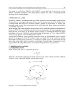
MLCC and a percolative composite is presented in Fig. 1. Unfortunately, the percolative
Ferroelectrics - Characterization and Modeling
118
approach in developing high dielectric constant materials has up to now very often been
handicapped by the impossibility of preparing homogeneous metal−insulator composites
with metal concentrations very close to the percolation threshold.
Fig. 1. Schematic configuration of a multilayer ceramic capacitor (MLCC) (left; 1-metallic
electrodes, 2-thin layers of dielectric/ferroelectric ceramics, 3-metallic contacts) and a
percolative composite (right; yellow and blue regions represent conductive and
dielectric/ferroelectric material, respectively).
Exceptionally high dielectric constants which were obtained by making use of the
conductive percolative phenomenon in ceramic composites made of perovskite ruthenium-
based conductive ceramics and perovskite ferroelectric ceramics, are reported in this
chapter. The potential of these all-ceramic percolative composites for use as high dielectric
constant materials in various applications is demonstrated: Due to a homogeneous
distribution of conductive ceramic grains within the ferroelectric ceramic matrix, the
dielectric response of the lead-based Pb(Zr,Ti)O
3
–Pb
2
Ru
2
O
6.5
and 0.65Pb(Mg
1/3
Nb
2/3
)O
3
-
0.35PbTiO
3
–Pb
2
Ru
2
O
6.5
as well as of the lead-free (K,Na)NbO
3
–RuO
2
systems namely
follows the predictions of the percolation theory. Thus, values of the dielectric constant are
near the percolation threshold for two orders of magnitude higher than in the pure matrix
ferroelectric ceramics.
2. Percolative composites
The theory of percolation was initially developed to describe several abrupt transitions
commonly found in transport phenomena. Based on this model, a general theory was built
that explains a physical process in which a macroscopic magnitude is strongly modified as a
result of small microscopic changes in connectivity (Feng et al., 1987). One such process is
the anomalous behavior of a metal-insulator composite near its percolation threshold, which
is characterized by an abrupt discontinuity in the real part of the electrical conductivity
(Bergman & Imry, 1977; Kirkpatrick, 1973). An excellent review for the system consisting of
randomly distributed metallic and dielectric regions is given in the paper of Efros and
Shklovskii (Efros & Shklovskii, 1976): It is shown that the static dielectric constant diverges
at the percolation threshold – at the volume fraction of metallic regions (p) where the
insulator-to-metal transition occurs, i.e., the static effective electrical conductivity σ of such a
heterogeneous system undergoes a transition from
σ
=
σ
matrix
[(p
c
-p)/p
c
]
-q
, (1)
which is valid below the percolation threshold p
c
, into