Advances in Satellite Communications Part 11 pot
Bạn đang xem bản rút gọn của tài liệu. Xem và tải ngay bản đầy đủ của tài liệu tại đây (1.1 MB, 15 trang )
Passive Microwave Feed Chains for High Capacity Satellite Communications Systems
139
parallel-plate waveguide. It is worth mentioning that since the EM field inside a generic
component can deviate significantly from the TEM field in a plane parallel-plate waveguide,
the rigorous analysis of the multipaction breakdown would require extensive numerical
computations of the electronic trajectories inside the devices in order to establish if an
avalanche of secondary-emission electrons can occur (Anza, et al., 2008)-(Tienda, et al, 2006).
Fig. 3.2. Envelope over all the resonance order of the minimum multipactor threshold
voltage
0
V as a function of the gap-frequency product fd for a silver-plated parallel-plate
waveguide.
Fig. 3.3. Transmission coefficient
21
()Tfof the E-plane WR75-waveguide symmetric stub-
filter shown in the insert (the inside waveguide structure of the filter is reported).
However, according to the ESA recommendations, the qualification process of a generic RF
component in terms of the power-handling under both single- and multi-carrier operating
10 11 12 13 14 15
-50
0
50
100
frequency (GHz)
T
21
(dB)
y
z
x
Advances in Satellite Communications
140
conditions can be carried out by evaluating an upper-bound on the multipaction risk and
setting appropriate confidence margins. In particular, the actual upper-bound is computed
by using the plane parallel-plate model along several directions inside the component. For
sake of clarity and without loss of generality, this procedure is described next by referring to
the E-plane WR75-waveguide symmetric stub-filter depicted in the insert of Fig. 3.3, where
the transmission coefficient
21
()Tf of this filter is reported. The transmission coefficient is
the relevant characteristic function of the filter, since it is equal to the ratio
11 21
()/ ()Sf Sf
where
11
()Sf is the scattering reflection coefficient at the input port, and
21
()Sf is the
scattering transmission coefficient from one port to the other. Hence, the transmission
coefficient
21
()Tf is proportional to the reflection coefficient in the pass-band and to the
inverse of the transmission between the two ports in the stop-band (isolation). The E-plane
stub architecture is commonly adopted in the Tx-channels of multiplexers (Tx-band = [10.7,
12.75] GHz) to block the Rx signals (Rx-band = [13.5, 14.5] GHz), since each stub exhibits a
transmission zero that can be adjusted in the stop-band by varying its length. In this way,
high levels of isolation can be achieved in the Rx-band along with very low standing-wave
ratio inside the component in the Tx-band. The latter condition can be exploited in order to
maximize the power-handling capability of these components.
Since this filter is an E-plane structure, the maximum electric field arises in the central plane
x=0, for which the in-phase field lines at 13 GHz are depicted in Fig. 3.4. Although the field
in the device is not everywhere oriented along straight lines connecting two parallel surfaces
(as in the parallel-plate model), it is possible to define a parallel-plate model for each of the
lines highlighted in cyan in Fig. 3.4. For this propose, the equivalent voltage
1
0
ˆ
() (;)
d
i
Vf Esf sds=⋅
(6)
is evaluated on the i-th integration line (oriented along
ˆ
s ). Moreover, the corresponding
multipaction threshold voltage
()thres
i
V for this section of the device, can be evaluated in
terms of the frequency-gap product fd
i by means of the susceptibility diagrams. For design
purposes, it is useful to introduce the voltage magnification factor
VMF
i
(Parikh, et al., 2003)
that provides a measure of the magnification of the electrical field occurring in the
i-th
position referred to the incident voltage V
(inc)
()
()
()
i
i
inc
V
f
VMF f
V
=
(7)
Accordingly, a breakdown-free condition is guaranteed at the
i-th section of the device if the
input power is smaller than the threshold level
()
2
()
2
||
()
2| |
thres
i
i
inc
i
V
Pf
ZVMF
= (8)
where
()inc
Z
is the power-voltage impedance at the input waveguide port. Finally, the
overall breakdown threshold power of the device at frequency
f is
()
() {()}
SC
i
i
P
f
min P
f
= (9)
Passive Microwave Feed Chains for High Capacity Satellite Communications Systems
141
Fig. 3.4. In-phase field lines in the plane x=0 of the E-plane WR75-waveguide symmetric
stub-filter shown in the insert of Fig. 3.3. The frequency is equal to 13 GHz. The lines
highlighted in cyan correspond to the integration lines used to define the equivalent
parallel-plate models.
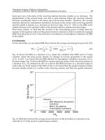
that clearly defines the power-handling capability of the component in a single-carrier
regime. Fig. 3.5 reports the frequency behavior of
()
()
SC
P
f
for the E-plane stub-filter in the
Tx-band. The minimum value of 2.6 kW at 12.75 GHz is due to the high levels of standing-
waves that are established inside the stubs at frequencies close to the -3 dB cut-off
frequency, in order to achieve high levels of isolation in the stop-band [13.5, 14.5] GHz. In
this regard, the power-handling capability of any device can be increased by adopting the
following strategies:
• Enlargement of the design bandwidth with respect to the actual operating bandwidth of
the device. In this way, as stated previously, the power-handling capability is not
adversely affected by very high standing-waves inside the component towards the
band limits.
• Application of surface-coating processes (i.e. silver-plating), since they guarantee higher
breakdown threshold voltages with respect to bare aluminum. It is worth mentioning
that the choice of the specific surface treatment has to be made by considering both the
insertion loss and the power-handling requirements.
• Setting proper constraints on the geometric parameters during the design of the
architecture. Indeed, a significant improvement in the power-handling capability can
be achieved by varying the height of the most critical sections of the component under
analysis. This leads to a larger frequency-gap product and, consequently, to higher
value of breakdown voltages. Hence, the geometrical parameters of the architecture are
determined through a trade-off process between the electrical requirements (e.g. return-
loss at the input ports or channel isolation) and the power-handling capability of the
y
z
Integration
lines
Advances in Satellite Communications
142
device. In this view, the design of novel instrumentation architectures exhibiting very
good electrical figure-of-merits along with very high power-handling capabilities is a
cutting-edge research topic for satellite communication systems.
Fig. 3.5. Single-carrier breakdown threshold power
()
()
SC
P
f
for the E-plane WR75-
waveguide symmetric stub-filter shown in the insert of Fig. 3.3.
On the basis of the single-carrier analysis previously described, it is possible to derive the
relevant design upper-bounds on the maximum power deliverable to the device operating
in a multi-carrier condition. Under the assumption of N carriers with equal power P, the
worst case corresponds to the in-phase sum of the carrier fields, thus leading to a total peak-
power equal to
2
NP. As a consequence, the breakdown-free condition in the device is
certainly guaranteed if the input power per carrier P is smaller than the threshold level
() ()
2
1
{()}
MC MC
f
PminP
f
N
= (10)
By considering a further margin of 3 or 6 dB, the standardized
2
" 6 dB"NP⋅+ or
2
" 3 dB"NP⋅+ rules are derived. Actually, these upper-bounds provide to be too strict
when a high number of carriers are considered. Indeed, the in-phase condition of the
N
carriers can be satisfied only for a short span of time. Moreover, the multipaction
breakdown is an electron secondary-emission resonance that has to be sustained by the
applied EM field. For these reasons, the in-phase matching condition becomes critical for the
multipactor breakdown only if it is satisfied for long time scales. In this respect, the high-
power qualification process of the devices operating in a multi-carrier regime is usually
carried out by adopting the more realistic “20-gap crossing” rule. The latter states that “as
10.5 11 11.5 12 12.5
0
5
10
15
20
25
frequency (GHz)
P
(S.C.)
(kW)]
Passive Microwave Feed Chains for High Capacity Satellite Communications Systems
143
long as the duration of the multi-carrier peak and the mode order gap are such that no more
than 20 gap-crossings can occur during the multi-carrier peak, the design may be considered
safe with regards to the multipaction breakdown even though the multipaction threshold
may be exceed from time to time”. Implementation of this rule in the case of
N linearly-
spaced carriers (frequency spacing
f
Δ ) yields the definition of the boundary function
(Parikh, et al., 2003).
()
20
1ln
V V
H
T
FN N
f
or N F N
T
=− − + < <
(11)
where
H
T is the period of multi-carrier envelope ( 1/
H
Tf=Δ) and
20
T is the time taken by
the electrons to cross the most critical gap 20 times. The latter parameter is equal to
20 0
(20 )/(2 )Tn
f
=× ×
, where n is the resonance order fulfilling the synchronism condition
and
f
0
is the lower frequency in the band of interest. On the basis of this boundary function,
the maximum power per carrier satisfying to the “20-gap crossing ” is
() ()
2
1
{()}
MC MC
f
V
PminP
f
F
= (12)
to which a further 6 dB confidence margin is commonly added, thus defining the “20-gap
crossing + 6 dB” rule. As an example, when considering 10 carriers linearly spaced in the
Tx-band of the E-plane stub filter, the maximum power per carrier according to this rule is
approximately 67 W.
3.2 Passive intermodulation products
Nonlinear characteristics in microwave components can lead to the generation of spurious
passive intermodulation products (PIMPs). When the intermodulation products of two or
more signals mixed in the device fall into the operative bandwidth of the receiver, this
intermodulation signal becomes an interference problem (Lui, 1990). As an example, if two
carriers with frequencies
f
1
and f
2
propagate through a nonlinear passive component, the
spurious intermodulation products are harmonics with frequencies
,12mn
f
m
f
n
f
=+ with m,
n integers. The sum
mn+ defines the order of the intermodulation product and the
amplitude of the PIMPs rapidly decay as a function of the order
mn+
. However, for the
case of considerable input power, some of the higher-order products can be great enough to
cause serious interference problems. This usually happens in satellite communication
systems where high-power transmitters and low-noise receivers are employed in the same
antenna-feed system. As a consequence, appropriate counter-measures have to be taken in
order to avoid the decrease of the signal-to-noise ratio in the Rx channels, which in turn
reduces the receivers sensibility. As an example, PIMPs level as low as -140 dB are
commonly required in Ku, K, Ka-band payloads operating broadcast and fixed satellite
services.
Generation of PIMPs take place mainly in the Tx power-amplifier circuits, in the receiver
mixers, and in the nonlinear metallic contacts inside the antenna-feed systems. The effects of
PIMPs generated in the back-end circuits (amplifiers and mixers) can be minimized by
inserting ad-hoc filters. On the contrary, PIMPs generated by possible metallic-oxide-
Advances in Satellite Communications
144
metallic contacts arising in the metallic mating surfaces of the front-end system components
are more troublesome. Indeed, depending on the specific position of the intermodulation
surface inside the antenna-feed chain, PIMPs can even not be filtered out. In this regard, the
level of PIMPs generated in an oxidized surface that mates two metallic blocks depends
significantly on the current through the junction. For this reason, the electrical and
mechanical designs of all the front-end components are strictly connected. Indeed, special
attention has to be paid when splitting a component in several blocks and in the connection
of the components.
With regards to the E- plane stub-filter described in Sec. 3.1, the clam-shell assembly shown
in Fig. 3.6 is a mechanical implementation of this device that is optimized In terms of PIMPs
generation. The device is halved in two blocks along the central plane x=0, thus allowing a
milling manufacturing of the inside waveguide structure. Since the currents in the central
plane x=0 are oriented along the longitudinal z-direction, no currents cross the two mating
surfaces, thus avoiding the generation of PIMPs. Finally, the PIMPs generated at the input
port sections, where the filter is connected to the other components, are minimized by
adopting a choke/plain joint consisting of a choke flange (applied to the filter) and a plain
flange (applied to the connecting device).
Fig. 3.7 shows the contour plot of the magnetic field amplitude inside the choke/plain joint
at 12.75 GHz. It is worth noting, that the magnetic field, hence the electric current, in the
contact point between the two flanges (named also cold point) is minimized with an
appropriate design of the resulting L-shaped radial stub. Moreover, the joint is designed to
exhibit a return-loss as high as possible in the operating bands (as high as 40 dB).
Fig. 3.6. Clam-shell mechanical assembly of the E-plane stub-filter shown in the insert of
Fig. 3.3.
Passive Microwave Feed Chains for High Capacity Satellite Communications Systems
145
Fig. 3.7. Contour plot of the magnetic field inside the L-shaped radial stub resulting from the
connection of the choke and plain flanges used to mount the filter of Fig. 3.6 with a
connecting device (a rainbow contour scale is used).
4. Broadband waveguide filters and diplexers
Metal waveguide filters are typically employed in satellite antenna-feed systems for their
low losses and high power-handling at the microwave frequencies. As discussed in the
introduction, these structures are mainly used to separate different sub-bands e.g. receive
and transmit bands as well as to protect the source from spurious signals. The latter
operation is usually performed using a single pass-band filter. The sub-band separation is
instead performed using two (or more) filters in the diplexer (multiplexer) configuration.
The same operation could be performed using a circulator, however, the diplexer solution
exhibits high-performance and a low-cost.
A general diplexer configuration is sketched in Fig. 4.1, where two different filters (TX and
RX) are connected to a three-port (T or Y) junction in order to obtain a common port (Port 1).
The other filter ports are instead connected to proper waveguide transitions to provide the
required orientation and size of Ports 2 and 3. More complex junctions could be adopted at
port 1 in order to increase the number of sub-bands.
Fig. 4.1. Scheme of a waveguide diplexer.
With reference to the diplexer architecture in Fig. 4.1, the basic electrical requirements are a
high transmission coefficient from Port 2 to Port 1, high attenuation from Port 2 to Port 3
and a low reflection coefficient at Port 2 in the TX frequency band. A high-transmission
connecting
device
filter
choke flange
contact
point
plain
flange
Advances in Satellite Communications
146
coefficient from Port 1 to Port 3, a high attenuation from Port 1 to Port 2, and a low-
reflection coefficient at port 3 have to be instead provided in the RX band. A low reflection
coefficient at Port 1 for both frequency bands is also required.
It should be pointed out that filtering structures with relatively broad pass-bands (more
than 5-10 %) are required owing to the present specifications of the satellite antenna feed
systems. For this reason, specific synthesis techniques based on distributed parameter
models and full-wave analysis tools should be adopted to design these kind of filters. These
filters and their corresponding design procedures are hence very different with respect to
narrow band (0.2-0.3 %) channel filters (not treated in this section) where the frequency
dispersion of the discontinuities around the pass-band is practically negligible.
The filters for the antenna feed system diplexers can be designed according to either the
pass-band or the stop-band architecture. Both of them can in principle be represented with
the fundamental-mode equivalent circuit of Fig. 4.2.
Fig. 4.2. Fundamental-mode transmission line equivalent circuit of a waveguide filter.
Such a circuit consists of N+1 scattering matrices
k
S , with
0, ,kN=
, connected by N
transmission lines representing the same number of generic waveguide discontinuities and
waveguide sections, respectively. The parameter l
k
defines the length of these sections.
In pass-band architectures, the filtering behavior is mainly related to the phase rotation
versus frequency in the N waveguide sections. In this framework, the latter are in fact
usually referred as cavities or resonators. The main role of the discontinuities is instead to
provide the required coupling between the adjacent resonators. However, as it will be
discussed in the following, the spurious dispersive effect of the various discontinuities
significantly affects the overall frequency behavior of the filter. Therefore, it should be kept
into account in the design stage.
As far the stop-band architecture is concerned, the required transmission zeros are
introduced by the discontinuities themselves, which exhibit a strong resonant behavior in
this case. The spacing between the various discontinuities is instead adjusted to obtain a
good matching in the pass-band.
The correct choice between the two architectures mainly depends on the overall required
frequency behavior i.e. the width of the pass-, stop- and transition bands, the power
handling capability, losses and the manufacturing complexity. Both the architectures will be
discussed in the remainder of this section.
4.1 Pass-band structures
Generally speaking, two class of discontinuities can be adopted in the design of pass-band
filters. The first one is represented by the transverse discontinuities i.e. inductive (Rozzi,
1972) or capacitive irises (Virone, et al. 2007). A band-pass configuration with inductive (or
Passive Microwave Feed Chains for High Capacity Satellite Communications Systems
147
H-plane) irises is shown in Fig. 4.3. As it can be seen, five resonators in rectangular
waveguide are obtained owing to the presence of the six inductive irises. The peculiarity of
this structure is the increased reflection coefficient of the irises at lower frequencies which
lead to very high attenuation levels in the frequency region below the pass-band. The
opposite phenomenon occurs with the capacitive configuration shown in Fig. 4.4. Indeed,
the reflection coefficient of capacitive irises increases at higher frequency providing a very
high attenuation above the pass-band of the whole filter. It has to be pointed out that
waveguide resonators with an increased height (see Fig. 4.4) are used to reduce the overall
losses.
For both the capacitive and inductive configurations, iris apertures and resonator lengths
are the main design parameters. The iris thickness is generally selected according to the
manufacturing materials and techniques. In particular, proper rounding of some of the filter
corners is also required when milling machines are adopted. Nevertheless, this feature can
be kept into account in modern design tools (Arndt, et al. 1997) in order to avoid the
insertion of tuning screws.
Fig. 4.3. Pass-band filter configuration with inductive (H-plane) irises.
Fig. 4.4. Pass-band filter configuration with capacitive (E-plane) irises.
Advances in Satellite Communications
148
The second class of discontinuities for pass-band filters is represented by the longitudinal
ones. Among these, the E-plane septum configuration shown in Fig. 4.5 is very popular
(Vahldieck, et al, 1983). Such a discontinuity provides a very high reflection coefficient
because the septum is placed in the middle of the waveguide where the electric field is
maximum. Moreover, the electromagnetic field is evanescent in the septum region owing to
the splitting of the main rectangular waveguide in two halves for which the TE10 is below-
cut off. The design parameters of the septum filter are both the resonator lengths and
septum lengths. The septum width is usually selected according to manufacturing
considerations. It should be pointed out that the septum reflection coefficient can even be
too high for certain broadband applications. Therefore, open septa can be adopted as first
and last discontinuities (Peverini, 2004). More advanced configurations feature ridge
waveguide resonators, instead of the common rectangular ones, in order to decrease the
overall length of the filter (Goussetis and Budimir, 2001).
Fig. 4.5. Pass-band filter configuration with E-plane septum discontinuities.
The evanescent mode filter is another common structure featuring longitudinal
discontinuities (Bornemann and Arndt, et al. 1990). As shown in Fig. 4.6, this configuration
is based on a dual ridge waveguide (single ridge versions are also used). Therefore, it leads
to more compact implementations in terms of both length and transverse section with
respect to the rectangular counterparts. The smaller transverse section also produce a wider
attenuation bandwidth. The small gap between the two ridges however generally reduce the
power handling of the structure owing to the multipactor phenomenon. The longitudinal
discontinuity is represented by the interruption of the ridge. In particular, the envelope of
the adopted ridge waveguide is selected so that the TE10 mode in the discontinuity region is
far below cut-off in the operative frequency band. In this way, a strong evanescent-mode
discontinuity is created. Besides the dimensions of the ridge waveguide, the relevant
parameters for the filter design are the lengths of both the resonators and the evanescent
mode sections.
Passive Microwave Feed Chains for High Capacity Satellite Communications Systems
149
Fig. 4.6. Evanescent mode filter.
As discussed above, all the filter geometries exhibit a large number of design parameters
that should be defined according to the required specifications on the frequency response. In
the past, this task has been generally accomplished on the basis of synthesis techniques for
lumped-parameters circuits and proper transformations (Levy, 1984). However, these
techniques do not take into account the frequency dispersion of both the discontinuities and
the cavities, the multimodal interactions and the losses which can significantly affect the
frequency response of a broadband filter. As a consequence, a considerable optimization
work is required to refine the initial solution. In particular, such an approach could lead to
sub-optimum designs owing to the presence of local minima in the pertaining cost function.
In order to overcome the above-mentioned problems, a design method based on both a
distributed-parameter model of the structure and a proper identification technique for the
various higher-order spurious effects has been developed (Tascone, et al. 2000). The method
exploits the single-mode circuit shown in Fig. 4.2, where each discontinuity is described
using its scattering parameters
() ()
11 21
,
kk
SS
and
()
22
k
S
. In the lossless case, these complex
quantities can be conveniently represented using the real parameter
k
γ
(
() ()
11 22
cos | || |
kk
k
SS
γ
==
and
()
21
sin | |
k
k
S
γ
= ) and the phases
()
11
k
ϕ
and
()
22
k
ϕ
. The resonators are instead described using
their lengths
k
l and the corresponding waveguide propagation constants
k
β
. It has been
demonstrated that the transmission matrix of the complete circuit can be written as
1
00
1
1, ,
0
csc cot
csc cot
cot csc
cot csc
k
k
j
kk
j
kn
k
kk
ze
T
ze
ψ
ψ
γγ
γγ
γγ
γγ
−
−
−
−
=
=
∏
where
(1) ()
1
11 22
exp{ [2 ( )]}
k
j
kk
kk
ze j l
ψ
βϕ ϕ
−
−
−
=− − + and
k
ψ
are unknown phase terms which have
been introduced in order to allow the synthesis of arbitrary frequency responses and to keep
the different phase behavior of the resonators into account. It should be noted that the
quantity
(1) ()
11 22
2( )
kk
kk
l
βϕ ϕ
−
−+ is the Round Trip Phase Shift of the resonators. It can be also
recognized that the elements of the transmission matrix
ࢀ are N-degree polynomials in the
complex variable
1
z
−
Advances in Satellite Communications
150
11
1
()
N
k
k
k
Tz az
−
=
=
and
21
1
()
N
k
k
k
Tz bz
−
=
=
As well-known, these parameters are related to the scattering matrix of the overall filter
11 11
1/TS= and
21 11 21
/TSS=
In particular, the
21
T parameter provides a very convenient description of the frequency
response in both the passband (where
21 11
TS≈
) and the attenuated bands (where
21 21
1/TS≈ ). Thanks to the polynomial representation, this single parameter can be used to
analytically define all the specifications of the filter in the same fashion as antenna arrays
and digital filter design techniques (FIR).
Once the polynomial
21
T has been defined according to the required specifications, an
extraction procedure is applied to determine the scattering matrix of the various
discontinuities (Tascone, et al. 2000) and the phase terms
k
ψ
. Starting from the electrical
parameters, the geometry of the discontinuities e.g. iris apertures, septum lengths are
obtained exploiting a pre-computed curve. The length of the various resonators
k
l is also
computed exploiting both the
k
ψ
and the
(1) ()
11 22
kk
ϕϕ
−
+ .
The synthesized geometry is then simulated using a full-wave method (e.g. Peverini, 2004).
As expected, the computed full-wave response is different from the synthesized polynomial
21
T
owing to the neglected phenomena in the synthesis model. Nevertheless, these
discrepancies can be properly compensated using the developed identification procedure
(Tascone, et al. 2000). Such a technique starts with the interpolation of the full-wave
response with a N-degree polynomial
21
1
()
N
k
k
k
Az cz
−
=
=
In this way, the overall procedure from the synthesis scheme to the analysis tool can be
represented as a single abstract system having the
21
()Tz
and
21
()
A
z
polynomials as input
and output, respectively. These quantities can be interpreted as periodic signals with
N
harmonics. Hence, their coefficients
k
b and
k
c can be considered as the discrete spectra of
these input and output signals, respectively. This approach leads to identification of the
above mentioned abstract system with a linear system, for which the transfer function
()Hz
can be defined as the ratio between the output and input spectra
/
kkk
hcb=
The introduced transfer function
()Hzproperly models the frequency dispersion of the
discontinuities, the multimodal interaction and the losses. Therefore, it can be used to
compute the coefficients a new “pre-distorted” frequency response
21
'( )Tz as
kkk
hbb /' =
Finally, the synthesis scheme discussed above is applied to this “pre-distorted” polynomial
/
kkk
hcb= to obtain the final filter geometry. Indeed, a single iteration is usually enough for
Passive Microwave Feed Chains for High Capacity Satellite Communications Systems
151
several considered filter designs. Anyway, some more iterations can be performed in
presence of highly-dispersive discontinuities or strong coupling to the evanescent modes.
The presented synthesis technique has been generalized to the design of waveguide
polarizers (Virone, et al. 2005) and waveguide diplexers (Virone, et al. 2009). For the latter,
the frequency response of a relevant design example for Digital Video Broadcasting
applications is reported in Fig. 4.7. It has been conceived with the capacitive iris
configuration (see Fig. 4.4). With reference to the port numbering reported in Fig. 4.1, the
reflection coefficient at common port (
11
S ) is below -30 dB for both the TX (10.95-12.75 GHz)
and RX (13.75-14.5 GHz) frequency bands. Similar reflection levels have been obtained at
both port 2 and 3 for the TX and RX bands, respectively. Due to the metallic losses, the
transmission coefficient is about -0.4 dB in the pass-band of both channels (an aluminum
prototype has been simulated). The isolation levels
21
1/S (from TX to port 1) and
31
1/S
(from 1 to RX) are higher than 55 dB in the RX and TX band, respectively. A level of 55 dB
has been obtained in both bands from TX to RX (
32
1/S ) as well.
Fig. 4.7. Waveguide diplexer with capacitive irises. The port numbering is reported in Fig.
4.1. The vertical dash-dotted lines represent the TX (10.95-12.75 GHz) and RX (13.75-14.5
GHz) frequency bands.
4.2 Stop-band structures
Strongly resonant waveguide discontinuities are required to design a stop-band filter. In
particular, they have to exhibit both a relatively wide transmission zero around the specified
stop-band and a moderate reflection level in the pass-band. A very common configuration is
the
E-plane stub in rectangular waveguide shown in Figs. 3.3-3.4. Several discontinuities
have to be cascaded to meet the specifications. The number of stubs is mainly related to the
10.5 11 11.5 12 12.5 13 13.5 14 14.5
-70
-60
-50
-40
-30
-20
-10
0
Frequency (GHz)
Magnitude (dB)
S
11
S
12
S
31
S
32
Advances in Satellite Communications
152
desired isolation level in the given bandwidth. Proper arranging of the various
discontinuities is mandatory to avoid degradation of the stop-band performance owing to
tunnel phenomena and strong multimode interactions. A significant design example of stub-
filter for satellite applications has already been described in section 3. Other designs can be
found in (Kirilenko, et al. 1994) and (Levy, 2009).
5. Ortho-Mode Transducers
A canonical Ortho-Mode Transducer (OMT) configuration has three physical waveguide
ports (see Fig. 5.1). The common port is a metallic waveguide having a two-fold symmetric
cross section (e.g. square or circular) which supports two degenerate modes i.e. two
orthogonal polarizations. Hence, two electrical ports should in fact be adopted to describe
the electromagnetic field at the common port. With reference to Fig. 5.1, the symbols V (H) is
hereinafter used to indicate the vertical (horizontal) polarization and Port 1 (2) is referred as
the electrical port of the component V (H). The two coupled ports are usually rectangular
waveguides operating in the single-mode regime. In other words, the OMT should in fact be
described using the four-port scattering matrix shown in Fig. 5.1 (Peverini, et al. 2006).
Fig. 5.8. The three waveguide ports of the OMT and the four-port scattering matrix
equivalent circuit.
An OMT waveguide architecture is conceived so that each of the two degenerate modes at
the common port is nominally coupled to one of the two single-mode ports only. According
to Fig. 5.1, Port 3 (4) is the coupled port of the component V (H). It means that the
magnitude of the direct scattering parameter S
31
(S
42
)
should be ideally equal to one. The
magnitude of the cross-coupling terms S
41
(S
32
) and the isolation terms S
21
and S
43
should
instead be zero.
According to a receive-mode operative condition, an OMT is therefore used to route the two
orthogonally polarized field components at the common port to two different waveguide
ports. By reciprocity, in transmit mode, an electrical signal excited at one of the two single-
mode ports is only routed to one of the two available polarizations at the common port.
The routing of the various signals is obtained introducing suitable apertures and
discontinuities between the common waveguide and the coupled waveguides. The isolation
Passive Microwave Feed Chains for High Capacity Satellite Communications Systems
153
between the two signals pertaining to the orthogonal polarizations is generally obtained
exploiting both the symmetry of the structure and particular cut-off phenomena.
Besides the isolation, other figures of merit of the OMT consist in power handling, insertion
loss, matching level, and low spurious higher-order-mode excitation at the four electrical
ports. Group delay equalization between the V and H channels is also required in some
specific applications. All the relevant electrical parameters of the OMT should be robust
with respect to the manufacturing tolerances. Manufacturing complexity, compactness and
proper orientation of the physical ports are also very important design parameters.
Several OMT configurations can be found in the literature. Their performances can change
significantly from both the electromagnetic and mechanical perspectives . The correct choice
highly depends on the application, however, it is worth mentioning that this choice strongly
affects the overall feed system topology. Therefore, it is important to correctly choose the
OMT since it drives the complexity as well as the cost and the dimension of the overall
antenna feed system.
The most interesting waveguide configurations for satellite communication systems will be
discussed in the following, starting from the basic ones up to the more recent and advanced
architectures. For the sake of simplicity, the square-waveguide common-port
implementations are only shown i.e. the V (H) polarization shown in Fig. 5.1 corresponds to
the TE10 (TE01) mode. Nevertheless, all the presented architectures can in principle be
extended to the circular cases.
5.1 Standard T-junction or side-coupling OMT
One of the simplest OMT architectures is represented by the T-junction shown in Fig. 5.2
(Schlegel and Fowler, 1984). The TE10 mode incident at the common port (carrying the
vertical polarization) propagates along the main arm (also called common waveguide) and
it is coupled to the fundamental mode of the rectangular port 3. The TE10 in the common
waveguide is not coupled to the fundamental TE10 at port 4 owing to both the symmetry of
the structure and the orthogonality of their field distributions.
Fig. 5.9. Standard T-junction OMT.