Biosensors Emerging Materials and Applications Part 8 pdf
Bạn đang xem bản rút gọn của tài liệu. Xem và tải ngay bản đầy đủ của tài liệu tại đây (4.81 MB, 40 trang )
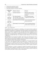
New Concepts of Integrated Photonic Biosensors Based on Porous Silicon
271
cleaning of the PSi devices to remove the remains from the patterning process, the PSi
structure is slightly thermally oxidized (≤ 1 nm SiO
2
) in order to enable subsequent silane-
based functionalization. The details of PSi functionalization are discussed in section 4.3. In
the following, we will consider the case of DNA sensing via hybridization of single-strand
DNA targets with their complementary strands immobilized on the PSi surface. After
immobilization of the DNA probes, the last required step is a capping to prevent non-
specific absorption. The main steps in the biosensor realization are summarized again
below:
anodization → patterning → oxidation → silanization → immobilization → capping →
hybridization.
The influence of each step on the optical properties of the PSi is characterized by reflectivity
measurements on 5 μm-thick PSi monolayers. After each step, the amounts of molecules
infiltrated inside the pores can be quantitatively evaluated by fitting the reflectivity spectra
with the refractive index models presented in section 5.1. The success of DNA
immobilization and hybridization has also been verified by fluorescence measurements
using probe and target molecules labelled with Cy3 and Cy5, respectively.
4.1 Porous silicon anodization
Anodization of silicon substrates to produce PSi is a well-described process in the literature.
It takes place in hydrofluoric acid (HF) solution, where the silicon is dissolved by the
fluorine ions thanks to the positive charges reaching the electrolyte/silicon interface
(Kochergin & Föll, 2009; Lehmann & Gösele, 1991). Depending on substrate doping, current
density and electrolyte concentration, the porosity and morphology of the fabricated PSi can
be varied (Lehmann et al., 2000). In particular, PSi structures constituted of successive layers
with different porosities, such as planar waveguides or multilayers, can be fabricated by
controlled variation of the current density during anodization.
Fig. 3a shows a schematic view of the cell used to prepare our PSi samples. In order to
fabricate meso-PSi, highly P-doped silicon substrates are used. The substrate is placed at the
bottom of the anodization cell on a copper electrode, and in contact with the
HF/H
2
O/ethanol (35%/35%/30%) electrolyte. The second electrode made of platinum is
immersed in the electrolyte at the top of the cell.
When preparing PSi layers for optical application, good care has to be taken that the
roughness at the interfaces between the layers is low enough to prevent light scattering.
Hence, anodization takes place at low temperature (-40°C) in order to enhance the viscosity
of the electrolyte, which has been shown to strongly reduce interface roughness (Setzu et al.,
1998). Working at low temperature also allows for a better control of the anodization
velocities, thus for a better control of the layer thicknesses. Fig. 3b presents a scanning
electron microscope (SEM) picture of a fabricated SW device consisting of PSi layers with
alternative porosities of 80% and 35% and a small surface layer with 35% porosity. In spite
of the roughness due to sample cleaving, very smooth interfaces between the layers can be
seen. The surface layer has a well-controlled thickness as thin as 60 nm.
After fabrication, the PSi structures are systematically characterized by reflectivity
measurements in the 900-1700 nm infra-red range, in order to check the porosity, layer
thickness and homogeneity. Fits of the reflectivity spectra are performed using the refractive
index models and the optical simulation methods presented in section 5.
Biosensors – Emerging Materials and Applications
272
Fig. 3. (a) Schematic view of the anodization cell used to prepare the PSi samples, and (b)
SEM picture showing an example of PSi multilayer.
4.2 Porous silicon patterning
After fabrication of the PSi layers, the next step in biosensor realization is PSi patterning to
build the PC devices. The challenge here consists in deeply patterning a material that is itself
nanostructured, anisotropic, and highly insulating, at a submicron scale. The desired air slits
should have perfectly vertical walls, a typical width of 200 to 400 nm, a period below 1 μm,
and an aspect ratio – i.e. depth/width ratio – of 2 to 4.
Different ways have been explored to obtain patterns in PSi at a submicron scale. Among
them, photo-dissolution appears to be a promising technique, which uses holographic
setups to create light patterns into the material and locally dissolve the material (Lerondel et
al., 1997). Similarly, photo-oxidation has also been proposed as an alternative to locally
oxidize and selectively etch patterns into PSi layers (Park et al., 2008).
Different nanoimprint techniques have also been proposed, such as soft lithography where
PSi is put in contact with a polymer stamp and selectively detached from the substrate
(Sirbuly et al., 2003). Very recently, patterning of PSi layers via nanoimprint using silicon
stamps has been proposed (Ryckman et al., 2010). This technique allows for the realization
of very well defined gratings; however, the PSi inside the patterns might get damaged. The
pattern aspect ratio that can be reached using imprinting techniques is also quite limited.
In order to reach the desired depth required for our PC devices, a patterning process based
on electron-beam lithography and reactive ion etching (RIE) has been selected. Very few
reports on PSi patterning using dry etching techniques can be found in literature. The
processes proposed are based on fluorine (Arens-Fischer et al., 2000; Tserepi et al., 2003) or
chlorine plasmas (Meade & Sailor, 2007) and have been used to realize patterns with widths
in the 10-100 μm range. In spite of these encouraging achievements, PSi patterning at sub-
micrometer scale with high aspect ratios remains a real challenge for many reasons: the
porous nanostructure of the material and its anisotropic morphology leading to poor
efficiency in the case of such directional etching processes, the large internal surface of PSi
favouring high sensitivity to contaminations such as polymer deposition during plasma
etching, as well as the strongly insulating nature of the material.
The different steps in the realization of the PSi PCs are presented in fig. 4. After fabrication
of the PSi by anodization, a silica layer is deposited by sputtering. This layer serves a triple
purpose, since it helps homogenising the surface of the sample for subsequent resist spin-
coating and lithography, it prevents the resist from penetrating into the material pores, and
New Concepts of Integrated Photonic Biosensors Based on Porous Silicon
273
it is used as a hard mask for RIE. After deposition of the silica layer, electron-beam
lithography is carried out using PMMA A4 resist, and the resist patterns are transferred into
the underlying silica layer by a CHF
3
-based RIE process. The patterned silica layer is then
used as a hard mask for PSi etching which occurs in SF
6
/Ar plasma.
Fig. 4. The different steps of the patterning process used to realize PCs in PSi.
After careful optimization of each step of the PC realization process, in particular PSi
patterning in SF
6
-based RIE, deep trenches with vertical walls and aspect ratio of about 2
were successfully etched into the PSi. Fig. 5a shows an example of trenches realized in a PSi
structure constituted of two layers with different porosity, 35% and 80% for the top and
bottom layer, respectively. It can be observed that the RIE process enables to etch both
porosities with perfectly vertical walls and no visible transition between the two layers in
spite of their very different morphological and electrical properties.
The etching efficiency of the RIE process strongly decreases with increasing porosity. Hence,
the pattern depth that can be reached is limited in the presence of 80% porosity layers, and
the process presented above has to be adapted to allow for the devices fabrication.
In the case of planar PC fabrication where only the top layer with 35% porosity is patterned,
the limitation in etching efficiency is induced by the presence of the underlying highly-
insulating 80%porosity substrate. In order to reach deeper patterns, anodization of the high-
porosity substrate can be performed after patterning of the top layer. Fig. 5b shows a SEM
view of a fabricated planar PC device which consists of a 700 nm-thick PSi layer with 35%
porosity on top of a substrate with 80% porosity. The width and period of the trenches are
400 nm and 900 nm, respectively. The high-porosity substrate was anodized after patterning
of the top layer. A very smooth interface between the two porous layers can be observed.
In the case of the SW device, much deeper trenches are required, since at least 3 multilayer
periods should be patterned. A well-known way to achieve deep etching is to use cyclic
processes including passivation steps to provide both sidewall verticality and protection of
the etching mask. However, such a process should be avoided in the case of PSi, as it would
lead to strong polymerization inside the PSi pores that would harden considerably the
material etching over time, as well as prohibit any subsequent biochemical
functionalization. In order to reach the desired number of patterned multilayer periods, a
new process using a more selective hard mask has to be developed. One way would be to
consider metallic masks; however, the issue of metal contamination of the internal PSi
surface exposed to the RIE environment has to be carefully investigated, as it may also
influence subsequent biochemical functionalization.
Biosensors – Emerging Materials and Applications
274
Fig. 5. (a) SEM image showing a preliminary result of patterning of PSi layers with different
porosities P1 (80%) and P2 (35%). (b) SEM images of fabricated planar PC in PSi. The period
of the patterns is 900 nm, and the device has a total size of 100 μm x 100 μm.
Another issue to tackle is the contamination of the PSi by fluorine during the RIE process.
Indeed, the fluorine contained in the plasma can react with inevitable carbon contamination
to form a fluorocarbon layer that deposits onto the PSi walls in the depth of the material.
Special treatments are currently under development to clean the PSi walls from this
contamination. Anodizing the substrate after RIE like in the case of the planar PC device is
also a good way to avoid this contamination.
4.3 Porous silicon functionalization for DNA sensing
The bioselective element of biosensors is usually based on the immobilization of
biomolecules on the surface of the transducer. The immobilization reaction can be achieved
by physisorption through weak interactions (van der Waals, coulombic forces), by
crosslinking with glutaraldehyde via an aminated surface (Rong et al., 2008) or SMCC via a
thiolated surface, by entrapment or by chemisorption via covalent bonding.
Covalent immobilization reactions of biomolecules require chemical functionalization of the
surface. These chemical groups can be introduced by plasma, polymer coatings… Hetero-
cross linkers are also widely used. These molecules have two functional groups: one
reacting with the material and one reacting with the biomolecules to be immobilized.
PSi has already been used as a large surface area matrix for immobilization of different
kinds of biomolecules including enzymes (Drott et al., 1997), DNA fragments (De Stefano et
al., 2007) and antibodies (Betty, 2009). Chemical functionalization of PSi can either involve
the native Si-H terminated surfaces or the Si-O bond resulting from PSi oxidation.
Native Si-H surfaces can lead to Si-C or Si-Si bonds via organometallic reactions or via
dehydrogenative silane coupling, respectively (Stewart & Buriak, 2000). The hydrosilylation
reaction of alkyne and alkene with Si-H leads to the formation of Si-C bond with reduction
of the C-C multiple bond. It proceeds with appreciable rate in the presence of white light,
Lewis acid or by thermal activation. Similarly, formation of Si-C can be obtained by reaction
of Grignard (Stewart & Buriak, 2000) or by electrografting reactions with organo halide
(Gurtner et al., 1999) or alkyne (Robins et al., 1999). Si-C bonds can also be formed by
cleavage of Si-Si linkage by reacting organolithium (Kim & Laibinis, 1998) or by
electrochemical reduction of alkynes (Robins et al., 1999).
Oxidation of silicon results in the incorporation of oxygen, leading to a surface bearing
terminal silanol groups. These groups can readily react with silazane, alkoxy silane or
New Concepts of Integrated Photonic Biosensors Based on Porous Silicon
275
organo silyl halide to form a siloxane bridge Si-O-Si. Organo silane can be mono or
multifunctional (tri or di-chloro or -alkoxysilane). Multifunctional silane is usually preferred
due to its higher reactivity and because it can lead to lower non-specific binding.
Silanization with aminopropyl triethoxy silane or 3-glycidopropyl trimethoxy silane is well
documented in the literature (Dugas et al., 2010a).
With multifunctional silane, additional intermolecular dehydration reactions between
adjacent organo silanols lead to a 2D network. This polycondensation reaction needs to be
perfectly monitored, otherwise it will lead to an anarchic 3D network and consequently to
non-reproducible surface chemistry and obstruction of the PSi pores. An alternative solution
is the use of monofunctional silane. Indeed, in this case each silane molecule can only react
with the surface to form a siloxane bridge or with another silane molecule to form a dimer
(Dugas et al., 2010b). The dimer is eliminated by subsequent washing. Therefore, no
polymeric network is formed. The lower reactivity of monofunctional silane can be
compensated by the use of silazane groups allowing for the complete reaction of all surface
accessible silanols as demonstrated by Dugas (Dugas & Chevalier, 2003). The obtained layer
was demonstrated to be reproducible and stable under harsh conditions.
Our process uses a monofunctional silane, tert-butyl-11-(dimethylamino)silylundecanoate
which is an organo silazane bearing an ester function. Chemical functionalization of silica
(Bras et al., 2004), PSi (Bessueille et al., 2005) and glass have been reported using this
molecule from solution in pentane or from gas phase (Phaner-Goutorbe et al., 2011). As
illustrated in fig. 6, after silanization, the tert-butyl ester is converted into the corresponding
carboxylic acid by acidolysis in formic acid and activated with N-hydroxy succinimide. The
obtained NHS ester surfaces can be employed for amine coupling. The resulting surface has
a molecule density of 2x10
14
molecules/cm². Immobilization of amino-modified oligo-
nucleotide from diluted solution (25 µM) yielded to 3 – 4x10
11
strands/cm². Hybridization
yield with single stranded synthetic oligonucleotide is 10-20% (Dugas et al., 2004).
Fig. 6. Amino modified oligonucleotide are covalently immobilized by formation of an
amide bond. After surface silanization with the monovalent silane uses tert-butyl-11-
(dimethylamino)silylundecanoate (a), the tert-butyl ester group is removed leading to the
corresponding carboxylic function (b). Activation (c) with diisoprpyl carbodiimide/ N-
hydroxysuccinimide allows for the reaction with amino modified oliganucleotide (d)
leading to the formation of an amide bond.
The resulting covalent immobilization of oligonucleotides can withstand 25 successive
cycles of hybridization/denaturation (in 0.1 N NaOH) onto the same surface without
observing any degradation, as well as deprotection/oxidation steps performed during
Biosensors – Emerging Materials and Applications
276
phosphoramidite oligonucleotide synthesis (Bessueille et al., 2005; Cloarec et al., 2008).
Immobilization of peptides (Soultani-Vigneron et al., 2005), histones (El Khoury et al., 2010)
or carbohydrates (Chevolot et al., 2007; Moni et al., 2009; Zhang et al., 2009) has also been
achieved.
5. Modeling of optical properties
Modelling of PSi based PCs includes two different aspects: the calculation of the refractive
index, and the simulation of the optical properties. They are presented in the following.
5.1 Calculation of porous silicon refractive index
PSi is a composite medium with a pore size much smaller than the wavelength of light.
Hence, the dielectric response can be described through an effective dielectric function. A
complete review of the different isotropic and anisotropic models used for the calculation of
PSi refractive index has recently been published (Kochergin & Föll, 2009). In the isotropic
approximation, the main models used for the calculation of the effective dielectric function
are the Bruggeman and Landau Lifshitz Looyenga (LLL) effective medium approximations
(EMA) that can be defined by the following expressions (Bruggeman, 1935; Looyenga, 1965):
3
11 1
33 3
:0: ,1
2
ieff
ieffii
iSi Si
ieff
iii
Bruggeman f LLL f f
εε
εεεε
εε
−
==−+=
+
(1)
where f
i
and
ε
i
are the volume fraction and the complex dielectric function of material i,
respectively. The refractive index of materials is related to the permittivity
ε
with
ε
= n
2
. The
refractive indices of Si and SiO
2
can be obtained from the Palik handbook (Palik, 1998). As
the materials are used in their transparency domain, the variations of their refractive indices
with the wavelength are deduced from a Cauchy law, using the parameters given in table 1:
24
BC
nA
λλ
=+ +
A B C
Si 3.4227 0.1104 0.041
SiO
2
1.4213 0.0856 -0.0735
Table 1. Cauchy law and values of the Cauchy coefficients used for the modelling.
In order to consider absorption of light in the doped silicon substrate, variations of the
refractive index induced by free carriers absorption have to be taken into account. The
relation proposed by Soref is used (Soref & Bennett, 1987), which requires calculation of the
electron and holes mobilities depending on substrate doping (Sedra & Smith, 1997).
The models presented above have been implemented to fit experimental data, in particular
the reflectivity measurements performed on PSi layers. As an example, the reflectivity
spectra of a PSi monolayer before and after an oxidation step are plotted on fig. 7. The
parameters of the Bruggeman and LLL models and the thickness of the PSi monolayer are
obtained using a Levenberg Marquardt nonlinear fitting method (Press et al., 1992). The
results obtained using the Bruggeman and LLL models reproduce well the experimental
indices deduced from reflectivity measurements. For this particular sample, the PSi layer
was found to have an initial porosity of 70% and 73%, respectively, and a thickness of 4.735
and 4.741 μm, respectively, for the Bruggeman and LLL models. Both models gave a silica
New Concepts of Integrated Photonic Biosensors Based on Porous Silicon
277
fraction of 11% after oxidation. Hence, the fitted parameters are very close for both models,
with a relative variation below 5%.
Fig. 7. Evolution of the reflectivity of a PSi monolayer before (dash) and after (straight)
oxidation step. The experimental data has been fitted with the Bruggeman and LLL models.
In the following sections, the refractive indices will be determined using the LLL model.
Fitting all experimental data using the LLL model, we could evaluate that the volume
fractions of silica after oxidation correspond to the formation of a layer having a thickness of
1 nm on the internal PSi walls, for both porosities considered (35% and 80%). This is
consistent with the experimental calibrations of the oxidation process. Similarly, the volume
fractions of silane molecules deduced from the experimental spectra after silanization are
equivalent to the formation of dense layers with refractive index 1.4 and thickness around
1.7 nm covering the internal PSi walls. This layer thickness is similar for both porosities and
consistent with the developed length of the silane molecules used (~ 1.7 nm).
5.1 Simulation of optical properties
Numerical modelling is a major concern for the study of PC structures. Along the years, two
main approaches have emerged: the plane wave expansion (PWE) and the finite difference
in the time domain (FDTD) method.
The PWE method relies on the translation symmetry of the PC structure. The method
assumes a time harmonic evolution of the electromagnetic fields. In this case, the Maxwell
equations lead to the following general Helmoltz equation:
2
1
() ()
()
r
Hr Hr
rc
ω
ε
∇× ∇× =
(2)
where
H stands for the magnetic field,
ω
the pulsation and
ε
r
is the relative dielectric
permittivity.
This is an eigenvalue problem, which can be solved using a Fourier expansion along the
vectors of the reciprocal lattice. It leads to the dispersion relation
ω
=
ω
(k) where k(k
x
,k
y
,k
z
) is
the light wave vector. This approach enables a very efficient calculation of the band
diagram, giving information on photonic band gaps, group and phase velocity… of the
infinite periodic structure. However, this useful approach suffers from some limitations. In
its common formulation, it could not easily handle losses (lossy material, leaky modes…). In
Biosensors – Emerging Materials and Applications
278
the following sections, a free software package is used, MIT Photonic Bands (MPB) (Johnson
& Joannopoulos, 2001).
When it comes to real finite devices, the FDTD method is more suited. This method relies on
the discretization in time and space of the Maxwell equations (Taflove & Hagness, 2005):
11EH
Hand E
tt
εμ
∂∂
=∇× =−∇×
∂∂
(3)
where
E and H stand for the electric and magnetic field, respectively, and
ε
and
μ
for the
dielectric and magnetic permittivity, respectively.
The numerical experiments generally consist in sending an electromagnetic pulse onto the
structure and to monitor its response with time. A single simulation run is necessary to get
the frequency response thanks to the Fourier transform of the time response. It gives access
to the spectral response of the system (transmission, reflection). The ability of FDTD to solve
open problems is very useful for the study of microcavities and leaky modes. It gives access
to the quality factor (Q factor = λ/Δλ) of resonances. Moreover, an electromagnetic field map
at a given frequency could be easily obtained thanks to the discrete Fourier transform. As
this method has achieved its full maturity, it can handle dispersive and lossy materials, non-
uniform mesh, non-linear effects… Another interesting development is the implementation
of periodic boundary conditions which enable the study of infinite PCs. Compared to the
PWE, the FDTD method is less efficient; however, it allows for the study of leaky modes
(modes above the light line, i.e. in the free-state continuum). The FDTD method also
requires a lot of computing resources which are now available, thanks to ever evolving
microprocessor power, and it can be by nature easily parallelized.
6. Performance study of photonic-crystal-based biosensors
In this section, a performance study of the two PC-based biosensors is discussed, using the
tools and methods presented above. Both devices are considered for use in the infra-red
range at around 1300-1500 nm wavelength where absorption losses in the material can be
neglected. In this case, the main source of losses in PSi devices is expected to be scattering at
the interface of the silicon nanocrystallites (Ferrand & Romestain, 2000). Experimental
measurements show that the losses are only a few cm
-1
in this wavelength range and should
not alter significantly the sensor response. Therefore, we expect our theoretical predictions
to be in good agreement with experimental results.
6.1 Surface-wave biosensor
The very high sensitivity of the SW sensor in the 1D – i.e., unpatterned – configuration has
been demonstrated both theoretically and experimentally. In particular, we have observed
angular variations as large as 20° after grafting of amine molecules inside the PSi device
(Guillermain et al., 2007). In further studies, much smaller amounts of biomolecules were
considered, in order to evaluate the limit of detection of the biosensor. It was demonstrated
that convenient lateral patterning could enhance the sensitivity of the biosensor by an order
of magnitude (Jamois et al., 2010a). In these previous studies, we focussed on SW sensors
having a high-index surface layer with porosity 35%. Such porosity enables to reach very
high sensitivities due to very large PSi internal surface. However, due to the small pore size
(< 10 nm) sensing is limited to small biomolecules. In the following, we consider the case of
New Concepts of Integrated Photonic Biosensors Based on Porous Silicon
279
SW sensors having a surface layer with larger porosity 55%, which might yield a slightly
lower sensitivity due to smaller PSi internal surface, but enables sensing of larger molecules.
The devices consist of a multilayer with period a and standard porosities P1 = 80% and
P2 = 35%, respectively, with corresponding refractive indices n1 = 1.4 and n2 = 2.5 deduced
from the LLL model. The multilayer is terminated by a surface layer with porosity
P
surf
= 55% and refractive index 2.0. Fig. 8 shows the band diagram of the 1D PC for the
propagation direction parallel to the surface. As the 1D PC is homogeneous in the direction
of propagation, the bands of the 1D structure shown in fig. 8 are continuous. However, the
continuity of the bands can be broken by introducing a periodic perturbation. If a periodic
pattern is introduced in the direction of propagation, bands are back-folded at the edge of
the lateral Brillouin zone – for wave vectors k = π/a – resulting in local band flattening, i.e., a
strong decrease of light velocity. After careful optimization of both the multilayer and the
array of air slits, a 2D structure was obtained with a PBG large enough to assure a good
confinement of the SW. The optimized parameters of the resulting 2D PC are thicknesses
d1 = d2 = 0.5a for the multilayer, and w = 0.8a and a’ = 1.2a for the width and period of the
air slits, respectively. For a good comparison of the sensor performances, the layer
thicknesses are the same for the 1D sensor as for the 2D device. Because the surface mode
position within the PBG is highly sensitive to the thickness of the surface layer (Guillermain
et al., 2006), optimization of the surface layer thickness has also been necessary to position
the SW in the middle of the PBG and thus provide a good light confinement within the
surface layer. The optimized thickness of the surface layer is h = 0.4a for both 1D and 2D
devices. Fig. 8 shows the band structures for the optimized 1D and 2D SW devices.
Fig. 8. Simulated band structures (MPB) of the SW sensor in air environment for the
unpatterned (1D) and patterned (2D) configurations.
As plane-wave simulations consider a semi-infinite structure that is not experimentally
achievable, periodic FDTD simulations were also performed to evaluate the performances of
more realistic devices. Considering a multilayer consisting of 6 periods and varying the
depth of the air slits, it could be verified that the optical properties of the device do not vary
significantly with an increase of the slits depth, provided that the air slits are at least 3
multilayer periods deep. Hence, our band structure calculations can well describe the
expected device performances, if the depth of the patterns in the experimental 2D sensor
reaches 3 multilayer periods.
Biosensors – Emerging Materials and Applications
280
In order to demonstrate the high device sensitivity, a comparative study of the optical
response in the 1D and the 2D cases has been performed in air environment, considering as
an initial state a slightly oxidized porous structure (~ 1 nm SiO
2
) and varying the amount of
molecules grafted onto the pore walls. Note that similar results would be obtained in the
case of specific biomolecular recognition, provided that the initial refractive index of PSi is
adjusted to take into account biochemical functionalization. Moreover, we consider the
limiting case where molecule grafting is restricted to the surface layer in order to take into
account the inhomogeneous infiltration of liquids and biomolecules inside meso-PSi, which
is the largest close to the surface and decreases in the depth of the multilayer, as was
demonstrated using labelled proteins (De Stefano & D’Auria, 2007). We should point out
that this restriction is underestimating the response of the biosensors.
The shift in the band structure induced by the grafting of 2.5%biomolecules inside the PSi is
presented in fig. 9 for both 1D and 2D devices. It can be seen that the much flatter surface
band of the 2D sensor leads to much larger variations in wave vector and in resulting
coupling angle. In the presence of the biomolecules, the shift in coupling angle is 0.7° for the
unpatterned device and as large as 4.0° for the patterned sensor. This corresponds to an
increase in sensitivity of the 2D device by a factor 6 compared to the 1D case.
Fig. 9. Optical response of the surface wave sensor to the grafting of 2.5% biomolecules in air
environment for the unpatterned (1D) and patterned (2D) configurations.
The variation in coupling angle and in refractive index depending on the amount of
biomolecules is presented in fig. 10 for the 2D biosensor. For a better understanding of the
amount of biomolecules infiltrated inside the pores, it is also expressed as the equivalent
thickness d
bio
of a dense monolayer having the same volume and homogeneously coating
the internal surface of the pores. This formalism has already been used in other studies of
photonic sensors based on PSi, and has proven to yield good agreement between theoretical
predictions and experimental results (Ouyang et al., 2006). As can be seen in fig. 10a, a
variation in coupling angle as large as 13.5° is expected for the grafting of a dense
monolayer of biomolecules with thickness 1.7, which corresponds to the case of our
silanization process. A much smaller amount of molecules of 0.1% – equivalent to a dense
layer with thickness 0.01 nm – would still induce a variation in coupling angle of 1°, with a
corresponding variation in refractive index of 6x10
-4
. Considering that high-performance
SPR setups can detect angular variations as small as 0.001°, we can conclude that the limit of
detection of the SW sensor is very low.
New Concepts of Integrated Photonic Biosensors Based on Porous Silicon
281
Fig. 10. Simulated optical response (MPB) of the SW sensor in air environment as a function
of the amount of detected biomolecules: (a) for large amounts, and (b) for smaller amounts.
The optical response is expressed both as a shift in coupling angle (Δθ) and as the
corresponding refractive index variation in the top layer (Δn). The amount of biomolecules
is given as a volume fraction inside the PSi (f
bio
) and as an equivalent thickness (d
bio
). The
blue dashed line indicates the expected device response to silane grafting.
6.2 Planar photonic-crystal biosensor
The optical response of the planar PC observed at normal incidence shows the superposition
between interferences occurring inside the PSi layers and the excited Fano resonances. In
order to maximize the variation of reflection induced by biosensing events, the structure has
to be optimized to position the resonance in a zero of reflectivity corresponding to
destructive interferences within the PSi layers. This way, the reflected signal at resonance
can be switched between 0% and 100%. The device optimization was performed combining
plane-wave and FDTD simulations for the TE polarization where the electric field is parallel
to the slits (Jamois et al., 2010b). After optimization, the band structure presented in fig. 11a
was obtained, yielding a Fano resonance with very sharp features at a relative frequency
a/λ = 0.66 very close to the Γ point, where it can be excited at normal incidence. The Q factor
of the resonance can be as high as 1200 for the optimized 1D PC with top layer thickness
h = 0.75a and trench width w = 0.4a. Note that the Q factor is very sensitive to the thickness
of the top PSi layer: increasing or decreasing the thickness by only 50 nm results in a
reduction of the Q factor by several hundred. As our fabrication process enables a very good
control of the layer thicknesses, the sensitivity of the Q factor should not have a significant
impact on the device performances. The Q factor also strongly varies with the filling factor,
i.e., the relative width of the air slits, which means that the experimental fabrication process
should be carefully calibrated to obtain the desired slit widths.
In order to evaluate the performance of the device for biosensing, a similar study was
performed as in the case of the SW sensor, considering as an initial state a slightly oxidized
porous structure (~ 1 nm SiO
2
) and varying the amount of molecules grafted onto the pore
walls. Fig. 11b shows the shift of the resonance depending on the amount of biomolecules.
Due to the finesse of the resonance, the presence of only 0.35% biomolecules leads to a shift
of the resonance large enough to induce a dramatic decrease in reflectivity from 100% (green
curve) down to 32% (red curve). The wavelength variation of the resonance depending on
the amount of biomolecules is presented in fig. 12a-b, where the amount of biomolecules is
Biosensors – Emerging Materials and Applications
282
Fig. 11. (a) Band structure of the planar photonic crystal device (MPB simulation). The
resonance of interest for biosensing is marked by a purple circle. (b) Reflectivity behaviour
showing the resonance shift depending on the amount of biomolecules (FDTD simulation).
again expressed both as a volume fraction f
bio
and as an equivalent thickness d
bio
. The
corresponding refractive index variation of the top PSi layer is also shown. As this study is
performed in air environment, the wavelength variation is determined for an initial
resonance centred at 1500 nm. Fig. 12a highlights the very large sensitivity of the device;
indeed, in the case of grafting of a dense monolayer of silane molecules with a length of
1.7 nm, the expected shift of the resonance is larger than 50 nm. Fig. 12b demonstrates that
smaller amounts of biomolecules can be well detected as well, since the grafting of 0.35% of
molecules – equivalent to a dense monolayer with only 0.02 nm thickness – would induce a
wavelength shift larger than 1 nm, which is in good agreement with fig. 11b. The induced
refractive index variation for this small amount of biomolecules would be below 2x10
-3
.
In order to evaluate the performances of the sensor for in-situ measurements, the same
study has been performed in aqueous environment. In this case, all the pores of the PSi
layers as well as the trenches are completely filled with water. The presence of water inside
the pores induces an increase of the oxidized PSi refractive index to 2.52 and 1.63,
respectively, for the top layer and the substrate. Hence, the index contrasts remain quite
large between the layers of different porosities, as well as between the PSi and the water-
filled slits. After a new optimization of the photonic crystal to take into account the new
index configuration, a similar Fano resonance was found to yield a Q factor above 1000 if the
thickness of the top layer is adjusted to 0.8a. This means that the presence of water does not
dramatically alter the device performances. Fig. 12c-d shows the optical response of the
sensor in aqueous environment with varying amount of biomolecules. For a better
comparison with the results obtained in air environment, the wavelength shifts have been
calculated for a resonance centred at 1500 nm. When using the device at shorter wavelength
(e.g., at 1300 nm where water absorption is strongly reduced) the wavelength shift of the
resonance is correspondingly slightly smaller. Due to the lower refractive index difference
between biomolecules and water (Δn < 0.1) than between biomolecules and air (Δn ~ 1.4), it
is expected that the same volume of molecules induces a lower optical response in aqueous
environment. In this case, silane grafting shown in fig. 12c would induce a shift of the
New Concepts of Integrated Photonic Biosensors Based on Porous Silicon
283
Fig. 12. Simulated optical response (MPB) of the planar photonic crystal biosensor in air and
aqueous environment, respectively: (a), (c) for large amounts of biomolecules, and (b), (d)
for smaller amounts. The optical response is expressed both in wavelength shift (Δλ) and in
corresponding refractive index variation in the top layer (Δn). The amount of biomolecules
is given as a volume fraction (f
bio
) and as an equivalent thickness (d
bio
). The blue dashed line
indicates the expected device response to silane grafting.
resonance by 7.5 nm, which corresponds to a decrease in sensitivity by a factor 7 compared
to the sensor in air environment. However, we can see in fig. 12d that very small amounts of
biomolecules can still be detected, as the grafting of 1% of biomolecules, equivalent to a
dense monolayer with 0.06 nm thickness, would induce a wavelength shift of 0.5 nm.
In order to study the experimental response of the biosensor, the process discussed in
section 4 was used to realize devices similar to the one shown in fig 5b. The fabricated
devices were then functionalized and their optical properties were characterized by
reflectivity measurements at each main functionalization step. The optical setup used for the
reflectivity measurements, presented in fig. 13a, is equipped with a wide band 1200-1600 nm
laser diode source and an InGaAs detector. Light is focussed on the 100 μm x 100 μm size
device via a microscope objective. Nano-positioning of the sample is achieved via an XYZ
piezoelectric table and is monitored with a visualization camera.
The optical response of the device is presented in fig. 13b. The green spectrum shows the
reflectivity of the device after oxidation. The oscillations in reflectivity due to the
interferences in the PSi substrate are clearly visible. Superimposed to these oscillations, 2
Biosensors – Emerging Materials and Applications
284
Fig. 13. (a) Schematic view of the optical setup. (b) Reflectivity measurements of the planar
PC device, after oxidation (green curve) and after subsequent silanization (red curve).
main resonances can be seen, the first one around 1280 nm and a sharper resonance at
1530 nm. This second resonance is the Fano resonance of interest for biosensing. After
silanization, the same device has been characterized again and the red spectrum has been
obtained. Comparing the two spectra, it can be observed that the interference fringes have
shifted, indicating a change in refractive index of the PSi layer and successful silane grafting.
Moreover, the second resonance that was initially at 1530 nm shows a strong 52 nm red
shift, which is in perfect agreement with the simulated expectations discussed in fig. 12.
After immobilization of DNA probes on the silanized PSi surface, the devices show strong
20 nm blue shifts, which are a signature of PSi corrosion due to remaining Si-H bonds
(Steinem et al., 2004). Although the amount of Si-H and Si-OH bonds is very low – almost
invisible on FTIR spectra – their presence is sufficient to induce a damage of the PSi
structure with the resulting blue shift, and to prevent any quantitative measurement of the
immobilized DNA molecules. Hence, both our oxidation process and the surface capping by
the silane molecules should be further improved to completely eliminate the Si-H bonds or
to prevent access from the water molecules to these H-bonds.
7. Conclusion
In this chapter, new concepts for meso-PSi integrated optical biosensors based on photonic
crystals have been presented, as well as the study of their performances.
The first biosensor is based on the excitation of SW at the surface of a PC device. Such
devices yield very high sensitivity that can be further enhanced by the introduction of lateral
patterning. We demonstrated a gain in sensitivity by a factor 6 between the 1D and 2D
biosensors. Another great property of this biosensor is the possibility to adjust the porosity
of the surface layer depending on the size of the target biomolecules. One disadvantage of
the SW device is that prism coupling requires large optical setups that are not convenient for
mass applications. It also requires large device areas and is not compatible with on-chip
multiple parallel sensing. These limitations can be overcome if the prism is replaced, e.g., by
a grating and if a detection principle similar to SPRI setups is used. The other limitation of
the SW sensor in its 2D configuration is a quite challenging technological realization due to
New Concepts of Integrated Photonic Biosensors Based on Porous Silicon
285
the depth of the slits that have to be patterned into the PSi multilayer. New processes are
currently been developed to enable the fabrication and experimental study of these sensors.
The second biosensor is based on the excitation of Fano resonances in planar PCs at normal
incidence. Such devices require simpler optical setups, they are very compact and can be
directly integrated into optical microchips, enabling for multiple parallel sensing. They yield
high sensitivity and their experimental realization is less challenging than in the case of SW
devices. We demonstrated perfect agreement between the theoretical and experimental
performances and shift of the resonance wavelength as large as 52 nm after grafting of a
silane monolayer. Because the porosity of the top layer cannot be too large in order to yield
good optical properties, these sensors are restricted to the detection of small biomolecules.
Further optimization of the sensor design will help to overcome this limitation.
Therefore, PCs in PSi are a very promising route to realize high performance biosensors that
can be fully integrated into optical microchips and used for in-situ analysis. As both the
experimental realization and the theoretical design of the devices are still at the focus of
intensive research, new exciting developments will certainly occur in a near future.
8. Acknowledgments
The experimental work is performed at the technological platform Nanolyon. R.
Mazurczyk, P. Crémillieu, C. Seassal, A. Sabac and J L. Leclercq are kindly acknowledged
for fruitful discussions on fabrication techniques and technical support. We are also very
grateful to C. Martinet, G. Grenet, C. Botella, N. Blanchard, P. Regreny and D. Leonard for
their help on physico-chemical characterization of PSi.
Financial support by the French ANR in the framework of the research project BiP BiP
(JC09_440814), and the INSA-Lyon in the framework of a BQR project, as well as the CSC for
PhD stipend funding are acknowledged.
9. References
Arens-Fischer, R.; Krüger, M.; Thönissen, M.; Ganse, V.; Hunkel, D.; Marso, M. & Lüth, H.
(2000). Formation of porous silicon filter structures with different properties on
small areas. Journal of Porous Materials, Vol. 7, pp. 223–225, ISSN 1380-2224
Bergveld, P. (1970). Development of an ion-sensitive solid state device for neurophysiolo-
gical measurements, IEEE Transactions on Biomedical Engineering Vol. 17, pp. 70–71
Bessueille, F.; Dugas, V.; Vikulov, V.; Cloarec, J P.; Souteyrand, E. & Martin, J.R. (2005).
Assessment of PSi substrate for well-characterised sensitive DNA chip implement.
Biosensors & Bioelectronics, Vol. 21, No. 6, pp. 908-916, ISSN 01694332
Betty, C.A. (2009). Highly sensitive capacitive immunosensor based on PSi-polyaniline
structure: Bias dependence on specificity. Biosensors and Bioelectronics, Vol. 25,
No. 2, pp. 338-343, ISSN 0956-5663
Bonanno, L.M. & DeLouise, L.A. (2007). Whole blood optical sensor. Biosensors &
Bioelectronics, Vol. 23, No. 3, pp. 444-448, ISSN 0956-5663
Bras, M.; Dugas, V.; Bessueille, F.; Cloarec, J P.; Martin, J.R.; Cabrera, M.; Chauvet, J P.;
Souteyard, E. & Garrigues, M. (2004). Optimisation of a silicon/silicon dioxide
substrate for a fluorescence DNA microarray. Biosensors and Bioelectronics, Vol. 20,
No. 4, pp. 797-806, ISSN 09565663
Biosensors – Emerging Materials and Applications
286
Bruggeman, D.A.G. (1935). Berechnung Verschiedener Physikalischer Konstanten von
Heterogenen Substanzen. Annalen der Physik, Vol. 24, pp. 636-664
Canham, L.T. (1990). Silicon quantum wire array fabrication by electrochemical and
chemical dissolution of wafers. Applied Physics Letters, Vol. 57, No. 10, pp. 1046-
1048, ISSN 0003-6951
Caras, S. & Janata, J. (1980). Field effect transistor sensitive to penicillin. Analytical Chemistry,
Vol. 52, No. 12, pp. 1935-1937, ISSN 0003-2700
Chapron, J.; Alekseev, S.A.; Lysenko, V.; Zaitsev, V.N. & Barbier, D. (2007). Analysis of
interaction between chemical agents and porous Si nanostructures using optical
sensing properties of infra-red Rugate filters. Sensors and Actuators B, Vol. 120,
No. 2, pp. 706-711, ISSN 0925-4005
Chevolot, Y.; Bouillon, C.; Vidal, S.; Morvan, F.; Meyer, A.; Cloarec, J P.; Jochum, A.; Praly,
J P.; Vasseur, J J. & Souteyrand, E. (2007). DNA-Based Carbohydrate Biochips: A
Platform for Surface Glyco-Engineering. Angewandte Chemie-International Edition,
Vol. 46, No. 14, pp. 2398-2402, ISSN 1433-7851
Cloarec, J P.; Chevolot, Y.; Laurenceau, E.; Phaner-Goutorbe, M. & Souteyrand, E. (2008). A
multidisciplinary approach for molecular diagnostics based on biosensors and
microarrays. IRBM, Vol. 29, No. 2-3, pp. 105-127, ISSN 12979562
Cunin, F.; Schmedake, T. A.; Link, J.R.; Li, Y.Y.; Koh, J.; Bhatia, S.N. & Sailor, M.J. (2002).
Biomolecular screening with encoded porous-silicon photonic crystals. Nature
Materials, Vol. 1, No.1, pp. 39-41, ISSN 1476-1122
De Stefano, L.; Arcari, P.; Lamberti, A.; Sanges, C.; Rotiroti, L.; Rea, I. & Rendina, I. (2007).
DNA Optical Detection Based on PSi Technology: from Biosensors to Biochips.
Sensors, Vol. 7, No. 2, pp. 214-221, ISSN 1424-8220
De Stefano, L. & D’Auria, S. (2007). Confocal imaging of protein distributions in PSi optical
structures. Journal of Physics: Condensed Matter, Vol. 19, pp. 395009, ISSN 0953-8984
Drott, J.; Lindstrom, K.; Rosengren, L. & Laurell, T. (1997). PSi as the carrier matrix in
microstructured enzyme reactors yielding high enzyme activities. Journal of
Micromechanics and Microengineering, Vol. 7, No. 1, pp. 14-23, ISSN 0960-1317
Dugas, V. & Chevalier, Y. (2003). Surface hydroxylation and silane grafting on fumed and
thermal silica. Journal of Colloid and Interface Science, Vol. 264, No. 2, pp. 354-361,
ISSN 00219797
Dugas, V.; Depret, G.; Chevalier, B.; Nesme, X. & Souteyrand, E. (2004). Immobilization of
single-stranded DNA fragments to solid surfaces and their repeatable specific
hybridization: covalent binding or adsorption? Sensors and Actuators, B: Chemical,
Vol. 101, No. 1-2, pp. 112-121, ISSN 0925-4005
Dugas, V.; Elaissari, A. & Chevalier, Y. (2010a). Surface Sensitization Techniques and
Recognition Receptors Immobilization on Biosensors and Microarrays, Recognition
Receptors in Biosensors, M. Zourob, Springer Verlag, pp. 47-134, ISBN 978-1-4419-
0918-3, New York (USA)
Dugas, V.; Demesmay, C.; Chevolot, Y. & Souteyrand, E. (2010b). Use of Organosilanes in
Biosensors, Biotechnology in Agriculture, Industry and Medecine, Nova Science
Publishers, Inc., ISBN 978-1-61668-029-9, New York (USA)
El Khoury, G.; Laurenceau, E.; Chevolot, Y.; Merieux, Y.; Desbos, A.; Fabien, N.; Rigal, D.;
Souteyrand, E. & Cloarec, J P. (2010a). Development of miniaturized
immunoassay: Influence of surface chemistry and comparison with enzyme-linked
New Concepts of Integrated Photonic Biosensors Based on Porous Silicon
287
immunosorbent assay and Western blot. Analytical Biochemistry, Vol. 400, No. 1,
pp. 10-18, ISSN 0003-2697
Fan, X.; White, I.M.; Shopova, S.I.; Zhu, H.; Suter, J.D. & Sun, Y. (2008). Sensitive optical
biosensors for unlabeled targets: A review. Analytica Chimica Acta, Vol. 620, pp. 8-26
Ferrand, P. & Romestain, R. (2000). Optical losses in PSi waveguides in the near-infrared:
Effects of scattering. Applied Physics Letters, Vol. 77, pp. 3535-3537, ISSN 0003-6951
Guillermain, E.; Lysenko, V. & Benyattou, T. (2006). Surface wave photonic device based on
PSi multilayers. Journal of Luminescence, Vol. 121, pp. 319-321, ISSN 0022-2313
Guillermain, E.; Lysenko, V.; Oroubtchouk, R.; Benyattou, T.; Roux, S.; Pillonnet, A. &
Perriat, P. (2007). Bragg surface wave device based on PSi and its application for
sensing. Applied Physics Letters, Vol.90, No. 24, pp. 241116, ISSN 0003-6951
Gurtner, C.; Wun, A.W. & Sailor, M.J. (1999). Surface modification of PSi by electrochemical
reduction of organo halides. Angewandte Chemie-International Edition, Vol. 38,
No. 13-14, pp. 1966-1968, ISSN 1433-7851
Jamois, C.; Li, C.; Orobtchouk, R. & Benyattou, T. (2010a). Slow Bloch surface wave devices
on PSi for sensing applications. Photonics and Nanostructures: Fundamentals and
Applications, Vol. 8, No. 2, pp. 72-77, ISSN 1569-4410
Jamois, C.; Li, C.; Gerelli, E.; Chevolot, Y.; Monnier, V.; Skryshevskyi, R.; Orobtchouk, R.;
Souteyrand, E. & Benyattou, T. (2010b). Porous-silicon based planar photonic
crystals for sensing applications, Proceedings SPIE 7713, Conference on Photonic
Crystal Materials and Devices IX, 7713OU pp. 1-10, Brussels, Belgium, April 12-15,
2010, ISSN 0277-786X
Jane, A.; Dronov, R.; Hodges, A. & Völcker, N.H. (2009). Porous silicon biosensors on the
advance. Trends in Biotechnology, Vol. 27, No. 4, pp. 230-239, ISSN 0167-7799
Joannopoulos, J.D.; Meade, R.D. & Winn, J.N. (1995). Photonic crystals, molding the flow of
light. Princeton Academic Press, Princeton, NJ, ISBN 0-691-03744-2
Johnson, S.G., & Joannopoulos, J.D. (2001). Block-iterative frequency-domain methods for
Maxwell's equations in a planewave basis.
Optics Express, Vol. 8, No. 3, pp. 173-190,
ISSN 1094-4087
Kim, N.Y. & Laibinis, P.E. (1998). Derivatization of PSi by Grignard reagents at room
temperature. Journal of the American Chemical Society, Vol. 120, No. 18, pp. 4516-4517,
ISSN 0002-7863
Kochergin, V. & Föll, H. (2009). Porous Semiconductors Optical Properties and Applications.
Springer, ISBN 978-1-84882-577-2, London
Lehmann, V. & Gösele, U. (1991). Porous silicon formation: A quantum wire effect. Applied
Physics Letters, Vol. 58, No. 8, pp. 856-858, ISSN 0003-6951
Lehmann, V.; Stengl, R. & Luigart, A. (2000). On the morphology and the electrochemical
formation mechanism of mesoporous silicon. Materials Science and Engineering,
Vol. B 69–70, pp. 11-22, ISSN 0921-5107
Lerondel, G.; Setzu, S.; Thönissen, M. & Romestain, R. (1997). Holography in PSi. Journal of
Imaging Science and Technology, Vol. 41, No .5, pp. 468-473, ISSN 8750-9237
Lin, V.S.–Y.; Motesharei, K.; Dancil, K P.S.; Sailor, M.J. & Ghadiri, M.R. (1997). A porous
silicon-based optical interferometric biosensor. Science, Vol. 278, pp. 840-842
Liscidini, M. & Sipe, J.E. (2007). Enhancement of diffraction for biosensing applications via
Bloch surface waves. Applied Physics Letters, Vol. 91, pp. 253125, ISSN 0003-6951
Biosensors – Emerging Materials and Applications
288
Looyenga, H. (1965). Dielectric constants of heterogeneous mixtures. Physica, Vol. 31,
pp. 401–406
Martin, J.R.; Souteyrand, E.; Lawrence, M.F. & Mikkelsen, S.R. (1994). Procedure for the
analysis of biological substances in a conductive liquid medium (GENFET). 1994
French Patent n° 94 0868, US Patent Application: USSN 08/ 649,985
Mathew, F.P. & Alocilja, E.C. (2005) Porous silicon based biosensor for pathogen detection.
Biosensors and Bioelectronics, Vol. 20, No. 8, pp. 1656-1661, ISSN 0956-5663
Meade, S.O. & Sailor, M.J. (2007). Microfabrication of freestanding PSi particles containing
spectral barcodes, Physica Status Solidi, Vol. 1, No. 2, pp. R71–R73, ISSN 1862-6254
Moni, L.; Pourceau, G.; Zhang, J.; Meyer, A.; Vidal, S.; Souteyrand, E.; Dondoni, A.; Morvan,
F.; Chevolot, Y.; Vasseur, J J. & Marra, A. (2009). Design of Triazole-Tethered
Glycoclusters Exhibiting Three Different Spatial Arrangements and Comparative
Study of their Affinities towards PA-IL and RCA 120 by Using a DNA-Based
Glycoarray. Chembiochem, Vol. 10, No. 8, pp. 1369-1378, ISSN 1439-4227
Ouyang, H.; Striemer, C.C. & Fauchet, P.M. (2006). Quantitative analysis of the sensitivity of
PSi optical biosensors. Applied Physics Letters, Vol. 88, pp. 163108, ISSN 0003-6951
Palik, E.D. (1998). Handbook of optical constants of solids. Academic Press New York, ISBN 0-
12-544423-0
Park, H.; Dickerson, J.H; & Weiss, S.M. (2008). Spatially localized one-dimensional PSi
photonic crystals. Applied Physics Letters, Vol. 92, No. 1, pp. 011113, ISSN 0003-6951
Phaner-Goutorbe, M.; Dugas, V.; Chevolot, Y. & Souteyrand, E. (2011). Silanization of silica
and glass slides for DNA microarrays by Impregnation and Gas phase Protocols: A
comparative study. Material Science and Engineering C, Vol. 31, No. 2, pp. 384-390,
ISSN 0928-4931
Press, W.H.; Flannery, B.P.; Teukolsky, S.A. & Vetterling, W.T. (1992). Numerical Recipes in C:
The art of Scientific Computing. Cambridge University Press, ISBN 0-521-43108-5
Rendina, I.; Rea, I.; Rotiroti, L. & De Stefano, L. (2007). Porous silicon-based optical
biosensors and biochips. Physica E, Vol. 38, pp. 188-192, ISSN 1386-9477
Robins, E.G.; Stewart, M.P. & Buriak, J.M. (1999). Anodic and cathodic electrografting of
alkynes on PSi. Chemical Communications, No. 24, pp. 2479-2480, ISSN 1359-7345
Rong, G.; Najmaie, A.; Sipe, J.E. & Weiss, S.M. (2008). Nanoscale PSi waveguide for label-
free DNA sensing. Biosensors and Bioelectronics, Vol. 23, No. 10, pp. 1572-1576, ISSN
0956-5663
Rossi, A.M.; Wang, L.; Reipa, V & Murphy, T.E. (2007). Porous silicon biosensor for
detection of virus. Biosensors and Bioelectronics, Vol. 23, pp. 741-745, ISSN 0956-5663
Ryckman, J.D.; Liscidini, M.; Sipe, J.E. & Weiss, S.M. (2010). PSi structures for low-cost
diffraction-based biosensing. Applied Physics Letters, Vol. 96, pp. 171103
Sassolas, A.; Leca-Bouvier, B.D. & Blum, L.J. (2008). DNA Biosensors and Microarrays.
Chemical Reviews, Vol. 108, No. 1, pp. 109-139, ISSN 00092665
Sedra, A.S. & Smith, K.C. (1997). Microelectronics Circuits. 4th Edition, Oxford University
Press, ISBN 978-0195116632
Setzu, S.; Lerondel, G. & Romestain, R. (1998). Temperature effect on the roughness of the
formation interface of p-type PSi. Journal of Applied Physics, Vol. 84, No. 6, pp. 3129-
3133, ISSN 0021-8979
New Concepts of Integrated Photonic Biosensors Based on Porous Silicon
289
Shinn, M. & Robertson, W.M. (2005). Surface plasmon-like sensor based on surface
electromagnetic waves in a photonic band-gap material. Sensors and Actuators B,
Vol. 105, No. 2, pp. 360-364, ISSN 0925-4005
Sirbuly, D.J.; Lowman, J.M.; Scott, B.; Stucky, G.D & Buratto, S.K. (2003). Patterned
microstructures of PSi by dry-removal soft lithography. Advanced Materials, Vol. 15,
No. 2, pp. 149-152, ISSN 0935-9648
Song, M J.; Yun, D H.; Min, N K. & Hong, S I. (2006). Comparison of effective working
electrode areas on planar and porous silicon substrates for Cholesterol Biosensor.
Japanese Journal of Applied Physics, Vol. 45, N°9A, pp. 7197-7202, ISSN 0021-4922
Soref, R.A. & Bennett, B.R. (1987). Electrooptical effect in Silicon. IEEE Journal of Quantum
Electronics, Vol. 23, pp. 123-129, ISSN 0018-9197
Soultani-Vigneron, S.; Dugas, V.; Rouillat, M.H.; Fedolliere, J.; Duclos, M.C.; Vnuk, E.;
Phaner-Goutorbe, M.; Bulone, V.; Martin, J.R.; Wallach, J. & Cloarec, J P. (2005).
Immobilisation of oligo-peptidic probes for microarray implementation:
Characterisation by FTIR, Atomic Force Microscopy and 2D fluorescence. Journal Of
Chromatography B-Analytical Technologies In The Biomedical And Life Sciences, Vol. 822,
No. 1-2, pp. 304-310, ISSN 1570-0232
Souteyrand, E.; Cloarec, J P.; Martin, J.R.; Wilson, C; Lawrence, I.; Mikkelsen, S.R. &
Lawrence, M.F. (1997). Direct detection of the hybridization of specific DNA
sequences by field effect. Journal of Physical Chemistry, Vol. 101, No.15, pp.2980-2985
Souteyrand, E.; Chen, C.; Cloarec, J;-P.; Nesme, X.; Simonet, P.; Navarro, I. & Martin, J.R.
(2000). Comparison between the electrochemical and optoelectrochemical
impedance measurement for the detection of DNA hybridization. Applied
Biotechnology and Biochemistry, Vol. 89, pp. 195-207, ISSN 0273-2289
Steinem, C.; Janshoff, A.; Lin, V.S Y.; Völcker, N.H. & Ghadiri, M.R. (2004). DNA hybridiza-
tion-enhanced porous silicon corrosion: mechanistic investigations and prospect for
optical interferometric biosensing. Tetrahedron, Vol. 60, pp. 11259, ISSN 0040-4020
Stewart, M.P. & Buriak, J.M. (2000). Chemical and Biological Applications of PSi
Technology. Advanced Materials, Vol. 12, No. 12, pp. 859-869, ISSN 0935-9648
Taflove, A & Hagness, S.C. (2005). Computational Electrodynamics: The Finite-Difference Time-
Domain Method. Third Edition, Artech House, Boston, ISBN 978-1-58053-832-9
Thévenot, D.R.; Roth, K.; Durst, R.A. & Wilson, G.S. (1999). Electrochemical biosensors:
recommended definitions and classification. Pure and Applied Chemistry, Vol. 71,
No. 12, pp. 2333-2348, ISSN 0033-4545
Thust, M.; Schöning, M.J; Frohnhoff, S.; Arens-Fischer, R.; Kordos, P. & Lüth, H. (1996).
Porous silicon as a substrate material for potentiometric biosensors. Measurements
Science and Technology, Vol. 7, pp. 26-29, ISSN 0957-0233
Thust, M.; Schöning, M.J; Schroth, P.; Malkoc, U.; Dicker, C.I.; Steffen, A.; Kordos, P. & Lüth,
H. (1999). Enzyme immobilisation on planar and porous silicon substrates for
biosensors applications. Journal of molecular Catalysis B, Vol.7, pp.77, ISSN 1381-1177
Tinsley-Bown, A.M.; Canham, L.T.; Hollings, M.; Anderson, M.H.; Reeves, C.L.; Cox, T.I.;
Nicklin, S.; Squirrell, D.J.; Perkins, E.; Hutchinson, A.; Sailor, M.J. & Wun, A. (2000).
Tuning the Pore Size and Surface Chemistry of PSi for Immunoassays. Physica
Status Solidi (a), Vol. 182, No. 1, pp. 547-553, ISSN 0031-8965
Tserepi, A.; Tsamis, C.; Gogolides, E. & Nassiopoulou, A.G. (2003). Dry etching of PSi in
high density plasmas, Physica Status Solidi (a), Vol. 197, pp.163-167, ISSN: 0031-8965
Biosensors – Emerging Materials and Applications
290
Viktorovitch, P.; Drouard, E.; Garrigues, M ; Leclercq, J L.; Letartre, X.; Rojo-Romeo, P. &
Seassal, C. (2007). Photonic crystals: basic concepts and devices. Comptes Rendus
Physique, Vol.8, pp. 253-266
Viktorovitch, P.; Ben Bakir, B.; Boutami, S.; Leclercq, J L.; Letartre, X.; Rojo-Romeo, P.;
Seassal, C.; Zussy, M.; Di Cioccio, L. & Fedeli, J M. (2010). 3D harnessing of light
with 2.5D photonic crystals. Laser & Photonics Reviews, Vol.4, No.3, pp. 401–413
Völcker, N.H.; Alfonso, I. & Ghadiri, M.R. (2008). Catalyzed oxidative corrosion of porous
silicon used as an optical transducer for ligand–receptor interactions. ChemBioChem,
Vol.9, pp.1176-1186
Zhang, J.; Pourceau, G.; Meyer, A.; Vidal, S.; Praly, J P.; Souteyrand, E.; Vasseur, J J.;
Morvan, F. & Chevolot, Y. (2009a). DNA-directed immobilisation of glycomimetics
for glycoarrays application: Comparison with covalent immobilisation, and
development of an on-chip IC50 measurement assay. Biosensors and Bioelectronics,
Vol.24, No.8, pp. 2515, ISSN 0956-5663
15
Porous Silicon Sensors - from
Single Layers to Multilayer Structures
J.E. Lugo, M. Ocampo, R. Doti and J. Faubert
Visual Psychophysics and perception laboratory School of Optometry
University of Montreal
Canada
1. Introduction
1.1 Origin and discovery
Silicon, one of the more common elements in nature, is defined as a metalloid, which
corresponds to the number 14 in the Mendeleyev Periodic Table. It is heavier than Carbon
(element number 6 in the periodic table and a key component in biochemistry), but both
have chemical characteristics that are very close. Since human civilization began, volcanic
stones containing this metalloid in the form of dioxide were used to create the first tools and
weapons. Roman historian Plinio the Elder (23AD-79AD) mentioned the Silex-Silicis (silicon
stones) in one of his works as very hard stones. These roman words are the Latin origin of
the name Silicon (Tomkeieff, 1941).
J.J.Berzelius was credited for the discovery of this element in 1824 in Stockholm, Sweden,
but Gay-Lussac and Thenard had already prepared impure amorphous silicon by 1811.
After World War II, once the applied mechanical technology was ready to produce very
pure silicon wafers (under the form of monolithic crystals) and succeeded to manage the
problem of the surface impurities and contamination (Hull, 1999), the electronic industry
jumped from the Germanium diodes to the Silicon integrated circuits and metal-oxide-
semiconductor (MOS) microprocessors that helped man reach the Moon. In summary, it is
safe to say that Silicon’s role along our evolution extends from prehistoric times to the
exploration of the Solar System.
In 1956 at the U.S. Bell Laboratories, Arthur Uhlir Jr. and Ingeborg Uhlir while trying a new
technique for polishing Silicon crystalline wafers observed for the first time a red-green film
formed on the wafer surface (Kilian et al, 2009). Since the discovery of its luminescence
properties by Leigh Canham in 1990 (Kilian et al, 2009), researchers started to study the
nonlinear optical, electric and mechanical properties of this nanostructure. This effort has
permitted the fabrication of uniform porous layers with diameters as small as one
nanometer, and permitting an enormous inner surface density.
2. How to prepare porous silicon (p-Si)
Several techniques exist to form this structure from a pure Silicon crystalline wafer. The
most popular are: electrochemical etching, stain etching and photochemical etching. Here
we introduce two versions of the etching process (Anglin, n.d).
Biosensors – Emerging Materials and Applications
292
2.1 Electrochemical etching
As shown in the figure 1, we have a Si wafer (single crystalline) with the top face in contact
with a hydrofluoric acid solution and where an immersed platinum electrode is placed at
certain distance from the wafer and parallel to it. In the bottom face of the wafer we find a
flat metallic electrode that is in close electric contact. Between the two electrodes there is a
controlled voltage supply with its negative pole connected to the platinum immersed
electrode. A current is established from the anodic electrode (back of the wafer) and the
catodic electrode (platinum immersed). Modulating four variables: the intensity and interval
of application of this current, the HF solution concentration, and the concentration and type
of dopant previously applied to the Si wafer (type-n, type-p, or highly doped: type-pp and
type nn) it is then possible to control the porous size and p-Si layer geometric parameters, as
well as the number of layers. Dopant refers to a different element atom that replaces a
percentage of the Si atom inside the wafer and that is compatible with it in a
crystallographic way, but that presents an electron in excess (type n) or an electron lack
(type p). This introduces a number of properties that modify the material behavior when an
electric field is applied, mainly the resistivity, that will influence the etching process
performance. The electric current oxidizes the surface silicon atoms permitting a fluoride
attack on them generating the pores. It is also possible to create multilayer structures by
alternating different current densities. For instance, if we start making the first layer with a
current density J
1
then the final porosity (and the refractive index) is going to be
approximately determined by this current density. The electrochemical reaction time
determines the thickness. By switching the current density to a different value J
2
, something
amazing happens, the reaction continues mostly at the crystalline silicon interface, leaving
an almost intact first layer. Then the second layer will have a different refractive index and
thickness (if we readjust the reaction time). Porosity can be measured by gravimetrical
means. That is, the original crystalline silicon wafer is weighted first, then p-Si is formed and
the wafer is weighted again, finally the p-Si layer is removed by adding KOH (Potassium
hydroxide) and the wafer is weighted once more. With these three measurements is possible
to determine the porosity. To measure the thickness, SEM (scanning electronic microscopy)
techniques are normally used giving the best resolution and accuracy. Refractive index is
usually determined by optical interference methods, where the refractive index can be
estimated by taking adjacent maxima or minima from interference fringes coming from the
p-Si sample.
Stain etching: In this procedure the power supply action is replaced by the chemical oxidant
action of nitric acid. The reaction control is performed trough the addition of other
additives. Results are less homogeneous than those of the first process described, but they
still permit to have the material quality compatible with several applications.
3. Different types of p-Si sensors. Overview
Sensors allow our systems and devices to be in relation with the real events that we need to
register or control. So, precision (same response to the same stimuli: repeatability) and
accuracy (indicating magnitude value as close as possible to the real magnitude of the
stimulus to be sensed: minimum absolute error spread) are two main requirements for any
sensor when the industry selects its type or structure for market use. However, other
properties will define the success of a new kind of sensor in the market. These are:
Porous Silicon Sensors - from Single Layers to Multilayer Structures
293
Fig. 1. Experimental setup for porous silicon fabrication.
technological compatibility with the existing devices, geometric dimension requirements,
low noise insertion, ease of adjustment and setup, low power consumption, performance
standardization (linear if possible), low thermal or aging characteristic drifts, robustness,
reliability, low obsolescence, and very wide field of applications. P-Si is a material that
accomplishes all of these requirements with enough margins to think that it will become
increasingly popular in the short term.
For instance, integrated circuits (IC) are made of crystalline Silicon, which means it is fully
compatible for associating a p-Si sensor to any electronic device. The electrochemical
technology used to create a p-Si layer does not collide with the IC lithography. The
geometric dimensions required to create this type of sensor are sufficiently small to be
integrated in an IC. The homogeneity of the porous and its radius control (internal surface
density control) as well as its layer stability is improving very fast. We can create a vast
range of p-Si structures ranging from photonic crystals, a diffusive absorption electric
material, a characterized geometry surface chemical reactor material, etc. The number of
potential sensing applications is very large and is still growing daily (Angelucci et al, 1997).
In this section we present an overview of several types of p-Si sensors. Although not an
exhaustive description, we cover a wide range of applications to illustrate the possibilities of
putting the special characteristics of this material to work. We must consider that the p-Si
application field is object of new developments practically everyday.
3.1 P-Si Biosensors: optical properties changes
Medical automated diagnostic, specific biological fluid concentration dynamics and
molecular recognition are some of the expanding needs to be satisfied in the biomedical,
veterinary and food industry. All of them could be achieved by this kind of sensors.
Research in this field was pushed by the discovery of the light emission capacity of the p-Si
material (Cullis & Canham, 1991). The main consequence of this fact was considering the p-
Si optical properties changes to detect target substances in function of the ability to trap
molecules given by the boundary chemistry that occurs in the inner porous surface and its
special characteristics (800 m
2
per gram).
Biosensors – Emerging Materials and Applications
294
3.1.1 Refractive index transduction
The mechanism referred to the absorption or diffusion of a complex molecule substance into
the p-Si material could be complex and dependent on the geometry of the porous layer, the
surface chemistry activity and the physical conditions present. We will try an intuitive
simplified description of this type of detectors.
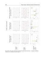
As shown in figure 2, a cell equipped with a transparent window contains a p-Si specimen
which surface is in contact with a solution flow. The window is swiped by a special fiber
optic tip linked to an interferometer. The fibers have two functions: a) providing white light
from a special lamp, and b) picking up the reflected light to send it into the interferometer
Fig. 2. Scheme showing the refractive index transduction.
that will let to obtain the System Reflectance Spectrum. This specific online info will give us,
by means of a computerized algorithm, the evolution in time of the p-Si refraction index n.
In this case the change in the reflectivity spectrum is a function of the DNA hybridization
between an immobilized reference DNA (molecules attached to the porous surface) and a
target DNA in solution (Jane et al, 2009). This event modifies the reflected light spectra in a
way that is suitable of being quantified, thus configuring a bio-sensor.
3.2 One-dimensional photonic crystals (1 D)
When the specimen structure corresponds to a one-plane multi layer p-Si crystal we are in
presence of a 1D photonic crystal (see figure 3). This geometry offers better reflectance
spectra (without side lobes) if compared with a mono-layer structure. Combining the layers
dimensions (layer thickness, porous density and radius, number of layers, etc.) we can tune
the different layer’s refraction index n, and according to the global geometry we can tune
the average refraction index, n
m
for the specimen. This kind of geometry permits create
Bragg reflectors and Micro cavities (Lee & Fauchet, 2009) which reflectivity shows defined
functional dependence when liquid solutions or gases are in contact with the p-Si specimen.
Once again the set up configuration is similar to the figure showing the fiber optic
interferometer. The figure below refers to the characteristic reflectance spectra for these two
Porous Silicon Sensors - from Single Layers to Multilayer Structures
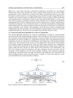
295
Fig. 3. Scheme showing two different one-dimensional photonic arrays of sensors.
types of photonic crystals. The difference between the incident light spectrum and the
Reflectance Spectrum is the energy absorbed (refracted light) by the crystal bulk (Jalkanen
et al, 2010). Finally, we would like to mention that this reflection mechanism shows in
addition another important characteristics as the polarization of the reflected light (TE or
TM) where the Transversal Electric or Transversal Magnetic components of the traveling
electromagnetic wave (in our case the incident light) are discriminated by the photonic
crystal reflection mechanism.
3.2.1 Reflectance spectrum shifting mechanism
The presence or absence of a target molecule in the liquid solution can be determined as
follows:
First, we obtain the reflected light spectrum with the device filled only with the solution
solvent: for instance: water (this is equivalent to zeroing our instrument). It will be the
reference reflectance spectrum.
In the next step we introduce into the liquid flow the substance containing the target
molecule, while computing the modified reflected light spectrum.
The modified spectra will be shifted (Baratto et al, 2002) in the light wavelength domain
with respect to the reference spectrum depending on:
- whether or not the solution is capable to go into the channels of p-Si, or it’s rejected
- the surface chemistry creates bonds that attach or not the target molecules against the
channels walls (this can be controlled by a previous surface oxidation)
- the type of bond attaching the molecules to the surface: ionic, covalent, etc.
-the refraction index of the substances involved, that is function of their solution
concentration and that depending on the device geometry will result in a global refraction
index valid for the device considered as an unit. In the figure 4, we present, as an example,
the detection two types of molecules together.