Optoelectronics Devices and Applications Part 1 pdf
Bạn đang xem bản rút gọn của tài liệu. Xem và tải ngay bản đầy đủ của tài liệu tại đây (1.33 MB, 40 trang )
OPTOELECTRONICS –
DEVICES AND
APPLICATIONS
Edited by Padmanabhan Predeep
Optoelectronics – Devices and Applications
Edited by Padmanabhan Predeep
Published by InTech
Janeza Trdine 9, 51000 Rijeka, Croatia
Copyright © 2011 InTech
All chapters are Open Access articles distributed under the Creative Commons
Non Commercial Share Alike Attribution 3.0 license, which permits to copy,
distribute, transmit, and adapt the work in any medium, so long as the original
work is properly cited. After this work has been published by InTech, authors
have the right to republish it, in whole or part, in any publication of which they
are the author, and to make other personal use of the work. Any republication,
referencing or personal use of the work must explicitly identify the original source.
Statements and opinions expressed in the chapters are these of the individual contributors
and not necessarily those of the editors or publisher. No responsibility is accepted
for the accuracy of information contained in the published articles. The publisher
assumes no responsibility for any damage or injury to persons or property arising out
of the use of any materials, instructions, methods or ideas contained in the book.
Publishing Process Manager Mirna Cvijic
Technical Editor Teodora Smiljanic
Cover Designer Jan Hyrat
Image Copyright john austin, 2010. Used under license from Shutterstock.com
First published September, 2011
Printed in Croatia
A free online edition of this book is available at www.intechopen.com
Additional hard copies can be obtained from
Optoelectronics – Devices and Applications, Edited by Padmanabhan Predeep
p. cm.
ISBN 978-953-307-576-1
free online editions of InTech
Books and Journals can be found at
www.intechopen.com
Contents
Preface IX
Part 1 Optoelectronic Devices 1
Chapter 1 Organic Light Emitting Diodes:
Device Physics and Effect of
Ambience on Performance Parameters 3
T.A. Shahul Hameed, P. Predeep, M.R. Baiju
Chapter 2 Integrating Micro-Photonic
Systems and MOEMS into Standard
Silicon CMOS Integrated Circuitry 23
Lukas W. Snyman
Chapter 3 SPSLs and Dilute-Nitride Optoelectronic Devices 51
Y Seyed Jalili
Chapter 4 Optoelectronic Plethysmography
for Measuring Rib Cage Distortion 79
Giulia Innocenti Bruni, Francesco Gigliotti and Giorgio Scano
Chapter 5 Development of Cost-Effective
Native Substrates for Gallium Nitride-Based
Optoelectronic Devices via Ammonothermal Growth 95
Tadao Hashimoto and Edward Letts
Chapter 6 Computational Design of
A New Class of Si-Based Optoelectronic Material 107
Meichun Huang
Part 2 Optoelectronic Sensors 129
Chapter 7 Coupling MEA Recordings
and Optical Stimulation:
New Optoelectronic Biosensors 131
Diego Ghezzi
VI Contents
Chapter 8 Detection of Optical Radiation in
NO
x
Optoelectronic Sensors Employing
Cavity Enhanced Absorption Spectroscopy 147
Jacek Wojtas
Chapter 9 Use of Optoelectronics to Measure Biosignals
Concurrently During Functional
Magnetic Resonance Imaging of the Brain 173
Bradley J MacIntosh, Fred Tam and Simon J Graham
Chapter 10 Applications and Optoelectronic
Methods of Detection of Ammonia 189
Paul Chambers, William B. Lyons, Tong Sun and
Kenneth T.V. Grattan
Chapter 11 Optical-Fiber Measurement
Systems for Medical Applications 205
Sergio Silvestri and Emiliano Schena
Part 3 Lasers in Optoelectronics 225
Chapter 12 The Vertical-Cavity Surface Emitting
Laser (VCSEL) and Electrical Access Contribution 227
Angelique Rissons and Jean-Claude Mollier
Chapter 13 Effects of Quantum-Well Base Geometry
on Optoelectronic Characteristics of Transistor Laser 255
Iman Taghavi and Hassan Kaatuzian
Chapter 14 Intersubband and Interband Absorptions in
Near-Surface Quantum Wells Under Intense Laser Field 275
Nicoleta Eseanu
Chapter 15 Using the Liquid Crystal Spatial
Light Modulators for Control of
Coherence and Polarization of Optical Beams 307
Andrey S. Ostrovsky, Carolina Rickenstorff-Parrao
and Miguel Á. Olvera-Santamaría
Chapter 16 Recent Developments in
High Power Semiconductor Diode Lasers 325
Li Zhong and Xiaoyu Ma
Part 4 Optical Switching Devices 349
Chapter 17 Energy Efficient
Semiconductor Optical Switch 351
Liping Sun and Michel Savoie
Contents VII
Chapter 18 On Fault-Tolerance and Bandwidth
Consumption Within Fiber-Optic Media Networks 369
Roman Messmer and Jörg Keller
Chapter 19 Integrated ASIC System and CMOS-MEMS
Thermally Actuated Optoelectronic
Switch Array for Communication Network 373
Jian-Chiun Liou
Part 5 Signals and Fields in Optoelectronic Devices 393
Chapter 20 Low Frequency Noise
as a Tool for OCDs Reliability Screening 395
Qiuzhan Zhou, Jian Gao and Dan’e Wu
Chapter 21 Electromechanical Fields in
Quantum Heterostructures and Superlattices 409
Lars Duggen and Morten Willatzen
Chapter 22 Optical Transmission Systems Using Polymeric Fibers 435
U. H. P. Fischer, M. Haupt and M. Joncic
Chapter 23 Transfer Over of Nonequilibrium Radiation
in Flames and High-Temperature Mediums 459
Nikolay Moskalenko, Almaz Zaripov, Nikolay Loktev,
Sergei Parzhin and Rustam Zagidullin
Chapter 24 Photopolarization Effect and Photoelectric
Phenomena in Layered GaAs Semiconductors 517
Yuo-Hsien Shiau
Chapter 25 Optoelectronics in Suppression Noise of Light 531
Jiangrui Gao, Kui Liu, Shuzhen Cui and Junxiang Zhang
Chapter 26 Anomalous Transient Photocurrent 543
Laigui Hu and Kunio Awaga
Part 6 Nanophotonics 563
Chapter 27 Nanophotonics for 21
st
Century 565
S. K. Ghoshal, M. R. Sahar, M. S. Rohani and Sunita Sharma
To my father; but for his unrelenting efforts I would not have made it to this day.
Preface
Optoelectronics - Devices and Applications is the second part of an edited anthology
on the multifaceted areas of optoelectronics by a selected group of authors including
promising novices to experts in the field, where are discussed design and fabrication
of device structures and the underlying phenomena. Many of the optoelectronic and
photonic effects are integrated into a vast array of devices and applications in
numerous combinations, and more are in fast development. New branches of
optoelectronics continues to sprout up such as military optoelectronics, medical
optoelectronics etc. The field of optoelectronics and photonics was originally aimed
at applying light to tasks that could previously only be solved through electronics,
such as in data transfer technology. Optoelectronics, being graduated to photonics
seeks to continue this endeavor and to expand upon it by searching for applications
for light. At any rate the optics related electronic and photonic phenomena, where
the closely connected players like electrons and photons, often refuse to be
demarcated into water tight compartments. With applications touching everyday
life and consumer electronic gadgets, optoelectronics is emerging as a popular
technology and draws from and contributes to several other fields, such as quantum
electronics and modern optics.
There are many aspects of light and its behavior that are important to those studying
electronics for scientific or industrial purposes. Light sensing is particularly important
in photonics, as the light involved in experiments and tests often needs to be
quantified and may not even be visible and electrons invariably helps in this. The role
of lasers in increasing the quality of life in modern times is unique. It is a lifesaving
source of light that enormously helped in medicine as in military technology and even
in entertainment, data storage, and holography.
The wide range of such applications in the field of optoelectronics and photonics
ensures that it is generally a well-funded and thriving area of scientific research and
upcoming researchers are sure to find it extremely encouraging. In the global energy
front also optics and photonics hold the hope of harnessing light to provide safe
energy and power especially in the light of the hidden dangers of nuclear power as an
alternative. I am sure that this collection of articles by experts from the field would
help them enormously to understand the underlying principles, design and fabrication
philosophy behind this wonderful technology. The first part of this set presents recent
X Preface
trends in the development of materials and techniques in optoelectronics and the
readers are suggested to have a look into that as well in the InTech websites.
July 2011
P. Predeep
Professor
Laboratory for Unconventional Electronics & Photonics
Department of Physics
National Institute of Technology Calicut
India
Part 1
Optoelectronic Devices
1
Organic Light Emitting Diodes:
Device Physics and Effect of Ambience
on Performance Parameters
T.A. Shahul Hameed
1
, P. Predeep
1
and M.R. Baiju
2
1
Laboratory for Unconventional Electronics and Photonics, National Institute of
Technology, Calicut, Kerala,
2
Department of Electronics and Communication, College of Engineering,
Trivandrum, Kerala,
India
1. Introduction
Research in Organic Light Emitting Diode (OLED) displays has been attaining greater
momentum for the last two decades obviously due to their capacity to form flexible (J. H.
Burroughes et al, 1990) multi color displays. Their potential advantages include easy
processing, robustness and inexpensive foundry (G.Yu & A.J.Heeger, 1997) compared to
inorganic counterparts. In fact, this new comer in display is rapidly moving from
fundamental research into industrial product, throwing many new challenges (J. Dane and
J.Gao, 2004; G. Dennler et al, 2006) like degradation and lifetime. In order to design suitable
structures for application specific displays, the studies pertaining to the device physics and
models are essentially important. Such studies will lead to the development of accurate and
reliable models of performance, design optimization, integration with existing platforms,
design of silicon driver circuitry and prevention of device degradation. More over, a clear
understanding on the device physics (W.Brutting et al, 2001) is necessary for optimizing the
electrical properties including balanced carrier injection (J.C.Scott et al, 1997: A.Benor et al.,
2010) and the location of the emission in the device. The degradation (J.C.Scott et al, 1996; J.
Dane and J.Gao, 2004) of the device is primarily caused by the moisture , which poses
questions to the reliability and life of this promising display. How the device responds to
different temperature ambience (T.W.Lee and O.Park, 2000) also attracts attention of
researchers since its applications at cryogenic temperature are yet to be explored. The basic
device physics and modeling philosophies based on the mathematical formulations of its
physical behavior are revisited in this article. Also it reviews the prominent ambient studies
and the efforts to enhance the reliability of the device by new fabrication methods with
inexpensive ways of encapsulation, making it suitable for long life display applications.
2. Principle and physics of organic LEDs
2.1 Device structure, principle
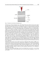
The simplest structure of OLED is shown in fig 1. The Tris(8-hydroxyquinolinato)
aluminium (Alq3) is an evaporated emissive layer on the top of spun cast hole transport
Optoelectronics – Devices and Applications
4
layer Poly-(3,4-ethyhylene dioxythiophene):poly-(styrenesulphonate) (PEDOT:PSS). Indium
Tin Oxide (ITO) and aluminium are the anode and cathode respectively. Charge injection,
transport and recombination (I.H.Campbell et al,1996) occur in the light emitting conductive
layer of organic light emitting diodes and its features influence efficiency and color of
emission from the device. Besides the characteristics of light emitting organic layer, interface
interactions (P.S.Davids et al, 1996) of this layer with other layers in OLED play important
role in defining the characteristics of the display. There have been innumerable studies on
different aspects of PEDOT: PSS (L.S.Roman et al,1999;S.Alem et al,2004) enhancing the
performance of photo cells and light emitting diodes. In practical implementations, more
layers for carrier injection and transport are normally incorporated.
Fig. 1. Structure of Organic Light Emitting Diode.
Fig. 2. Injection, Transport and Recombination in PLED[15].
In Polymer Light Emitting Diodes(PLED), conducting polymers like Poly (2-methoxy, 5-(2-
ethylhexoxy)-1, 4-phenylene-vinylene (MEH- PPV) are used as the emissive layer in which
dual carrier injection takes place (Fig. 2). Electrons are injected from cathode to the LUMO of
the polymer and holes are injected from anode to HOMO of the conducting polymer and
they recombine radiatively within the polymer to give off light (Y.Cao et al,1997). The
fabrication of the device is easy through spin casting of the carrier transport layer and
Electro Luminescent layer (MEH-PPV) for thickness in
o
A
range.
Organic Light Emitting Diodes:
Device Physics and Effect of Ambience on Performance Parameters
5
2.2 Device physics
For OLEDs, it is more often a practice to follow many concepts derived from inorganic
semiconductor physics. In fact, most of the organic materials used in LEDs form disordered
amorphous films without forming crystal lattice and hence the mechanisms used for
molecular crystals cannot be extended. Detailed study on device physics of organic diodes
based on aromatic amines (TPD) and aluminium chelate complex (Alq) was carried out by
many research groups (W.Brutting et al,2001).Basic steps in electroluminescence are shown
in fig. 3 where charge carrier injection, transport, exciton formation and recombination are
accounted in presence of built-in potential. Built-in potential(Vbi) across the organic layers is
due to the different work functions between anode and cathode (I.H.Campbell et al,1996).
Fig. 3. Basic Steps of Electroluminescence with Energy Band[4].
Built-in potential (Vbi) found out by photovoltaic nulling method, where OLED is
illuminated and an external voltage is applied till photocurrent is equal to dark current
(J.C.Scott et al,2000). Its physical significance is that it reduces the applied external voltage V
such that a net drift current in forward bias direction can only be achieved if V exceeds built
in voltage.Carrier injection is described by Fowler-Nordheim tunneling or Richardson-
Schottky thermionic emission, described by the equations
*2 2
3/2
22
2
exp( )
3
B
FN
BB
AqF
j
qF
K
(1)
*2
exp( )
BRS
RS
B
F
jAT
KT
(2)
The current is either space charge limited (SCLC) or trap charge limited (TCLC).The
recombination process in OLED has been described by Langevin theory because it is based
on a diffusive motion of positive and negative carriers in the attractive mutual Coulomb
field. To be more clear, the recombination constant (R) is proportional to the carrier mobility
(W.Brutting et al,2000).
0
[/ ][ ]
he
Rq
(3)
Apart from the discussion on the dependence of current on voltage and temperature, the
current has a direct dependence on the thickness of the organic layer and it was observed
that thinner the device better will be the current output. Similar observations were also
Optoelectronics – Devices and Applications
6
made by the group on J-V and luminance characteristics of ITO/TPD/AlQ/Ca hetero
junction devices for different organic layer thickness. The thickness dependence of current
at room temperature leads to the inference that the electron current in Alq device is
predominantly space charge limited with a field dependent charge carrier mobility and that
trapping in energetically distributed states is additionally involved at low voltage and
especially for thick layers. The temperature dependence of current in Al/Alq/Ca device
(from 120 K to 340K) indicates that device is having a less turn-on current at higher
temperature and recombination in OLED to be bimolecular process following the Langevin
theory. The mathematical analysis of the device, considering traps and temperature has
been a new approach in device physics.
Towards the search of highly efficient device, the combining of Alq and NPB, with a
thickness of 60nm for the Alq layer has been determined to yield higher quantum efficiency
whereas thickness variation of NPB layer doesn’t show any measurable effect.
The field and temperature dependence of the electron mobility in Alq leads to the delay
equation (W.Brutting et al,2000) as
d
d
t
F
(4)
where
bi
VV
F
d
.
The behavior of hopping transport in disordered organic solids has been better explained by
Gaussian Disorder Model (H.Bassler,1993). The quantitative model for device capacitance
with an equivalent circuit of hetero layer device gives more insight into interfacial charges
and electric field distribution in hetero layer devices.
The transport behavior in polymer semiconductor has been a matter of active debate since
many theories were put forwarded by different groups. Charge transport is not a coherent
motion of carriers in well defined bands - it is a stochastic process of hopping between
delocalized states, which leads to low carrier mobilities
2
(1/)cm Vs
(W.Brutting et
al,1999). Trap free limit for dual carrier device was studied by Bozano et al,1999. Space
charge limited current was observed above moderate voltages (>4V), while zero field
electron mobility is an order of magnitude lower than hole mobility. Balanced carrier
injection is one of the pre requisites for the optimal operation of single layer PLEDs.
Balanced carrier transport implies that injected electrons and holes have same drift
mobilities. In fact, it is difficult to achieve in single layer devices due to the predominance of
one of the carriers and hence bi-layer devices are used to circumvent the problem.
ITO/PPV/TPD: PC/Al devices fabricated where ITO/PPV is an ideal hole injecting contact
for the trap-free MDP TPD: PC. Here ITO/PPV contact acts as an infinite, non depletable
charge reservoir, which is able to satisfy the demand of the TPD: PC layer under trap-free
space-charge-limited (TFSCL) conditions (H.Antoniadis et al,1994). Trap free space charge
limited current (TFSL) [L.Bozano et al,1999) can be expressed as
2
0
9
/
8
TFSL
JEd
(5)
Organic Light Emitting Diodes:
Device Physics and Effect of Ambience on Performance Parameters
7
where
0
is the permittivity of vacuum,
is the permittivity of the polymer,
is the
mobility of holes in trap free polymer, d is inter electrode distance(M. A. Lampert and P.
Mark ,1970). Trapping is relatively severe at low electric fields and in thick PPV layers. At
high electric fields, trapping is minimized even for thick PPV layers.
The carrier drift distance x at a given electric field E before trapping occurs is given by
xE
where
is the trapping time. The electron deep trapping product
determines
the average carrier range per applied electric field before they get immobilized in deep
traps. It is imperative that the difference in
values of electrons and holes in PPV (
12
10
and
92
10 /cm v
respectively) reflects their discrepancy in transport. In fact, not the
structure of PPV contributes to this difference, but oxygen related impurities in PPV (P.K.
Konstadinidis et al,1994) with strong electron accepting character and reduction potential
lower than PPV may act as the predominant electron traps and limit the range of electrons.
The study of temperature dependence of current density versus electric field for single
carrier (both electron dominated and hole dominated) and dual carrier devices at
temperatures 200K and 300K exhibits interesting results (L.Bozano et al,1999). In both
temperatures, the reduction in space charge due to neutralization contributes to significant
enhancement in current density in dual carrier devices . Also it was deduced that the electric
field dependence of the mobility is significantly stronger for electrons than for holes. The
electric field coefficient
is related to temperature as per the empirical relation
0
(1/ 1/ )kT kT B
where B and
0
T are constants (W.D.Gill,1972). In MEH-PPV devices,
charge balance will be improved by cooling which in turn leads to enhanced quantum
efficiency. By adjusting barrier heights, at the level of 0.1eV, quantum efficiency close to
theoretical maximum can be achieved. In order to limit the space charge effects and hence to
enhance the performance in terms of current density, the intrinsic carrier mobility to be
taken care by modifying dielectric constant or electrically pulsing the device at an interval
greater than recombination time. The other means of improvisation is aligning of polymer
backbone, but such efforts may lead to quenching (L.Bozano et al,1998)
2.3 Device models
Device modeling is useful in many ways like optimization of design, integration with
existing tools, prediction of problems in process control and better understanding of
degradation mechanism. By modeling PLEDs current-voltage -luminance behavior, with
which quantum and power efficiencies can be analytically seen, this in turn normally has to
be subjected to experimental validation.
Both band based models and exciton based models were proposed to explain the
electronic structure and operation of polymer devices. Out of the two, there are more
supportive arguments for band based model. I.D.Parker examined (I.D.Parker,1994) the
factors that control carrier injection with a particular reference to tunneling, by
experimenting on ITO/MEH-PPV/Ca device. The thickness dependability of current
density with respect to bias and field strength are shown in fig.4 and 5 respectively. It is
obvious from these figures that the device operating voltage shall be reduced by reducing
the polymer thickness. The field dependence of I-V behavior points to the tunneling
model of carrier injection, in which carriers are field emitted through a barrier at
electrode/polymer interface (fig.4).
Optoelectronics – Devices and Applications
8
Fig. 4. Thickness Dependence of the I-V Characteristics in ITO/MEH-PPV/Ca Device
(I.D.Parker,1994).
Fig. 5. Field v Current Dependence for ITO/MEH-PPV/Ca Device ((I.D.Parker,1994).
For a clear understanding of the device physics and models, it is customary to fabricate
single carrier and dual carrier devices. On replacing Ca, having low work function (2.9eV)
with higher work function metals like In (4.2eV), Au (5.2eV), hole only devices can be made.
This increases the offset between Fermi energy of cathode and LUMO of polymer which
causes a substantial reduction in injected electrons and holes become dominant carriers. It is
apparent that the external quantum efficiency reduces in single carrier devices. The current
characteristics show only a slight dependence with temperature which is predicted by
Fowler-Nordheim tunneling.
2
exp( )
k
IF
F
(6)
where F is the field strength The constant k is defined by
*3/2
82
3
m
k
qh
(7)
Organic Light Emitting Diodes:
Device Physics and Effect of Ambience on Performance Parameters
9
where
is the barrier height and
*
m is the effective mass of the holes(S.M.Sze,1981).
A rigid band model better explains experimental results where holes and electrons tunnel
into the polymer when applied electric field tilts the polymer bands to present sufficiently
thin barriers. Fig.6 clearly indicates how this model envisages tunneling of holes.
Fig. 6. Band Diagram (in Forward Bias) for Model, indicating positions of Fermi Level for
different electrode materials (I.D.Parker,1994).
From the band based model and characterization, the improvements in device performance
was suggested by I.D. Parker. Of the devices he made, ITO/MEH-PPV/Ca devices exhibit
better results due to the reasons explained elsewhere. The device turn – on happens at a flat
band condition and it is in fact the voltage required to reach the flat-band condition and it
depends on the band gap of the polymer and work-function of electrodes. The operating
voltage of the device is sensitive to barrier height whereas the turn-on voltage is not.
From the equations mentioned before, an approximation for the current can be made as
2
exp( )I
V
(8)
where V is the applied voltage and
is the barrier height. This prediction of barrier height
dependence of operating voltage has been supported by experimental credentials.
Efficiency of the device is a function of current density due to minority carriers, increasing
barrier height leads to an exponential decrease in current and efficiency, which is shown in
fig.7.Parker had suggested the suitable combination of electrode materials and polymers so
that low turn-on voltage and operating voltage can be achieved.
J.C.Scott et al(J.C.Scott et al,2000) contributed to unveil the phenomena like built in
potential, charge transport, recombination and charge injection with a numerical model to
calculate the recombination profile in single and multilayer structures. ‘Essentially trap free’
transport, Langevin mechanism for recombination and model of thermionic injection with
Schottkey barrier at metal organic interface are the important features used by them. It is to
be highlighted that charge trapping is neglected in the analysis and transport is described in
terms of trap free space charge limited currents. Fowler-Nordheim mechanism was used to
explain the injection, but by analytical methods and simulations, thermionic injection ( G.G.
Malliaras ,1998) is said to best suit for explaining the injection in organic diodes.
Optoelectronics – Devices and Applications
10
Fig. 7. Device Efficiency v (Barrier Height)
3/2
[I.D.Parker,1994).
There are remarkable efforts (P.W.M.Blom & Marc J.M,1998) in characterization and
modeling of polymer light emitting diodes. Their experiments on PPV devices, both single
carrier and dual carrier devices, paved the way to the better understanding of mobility of
electrons and holes. Electron only devices are fabricated by a PPV layer sandwiched
between two Ca electrodes whereas hole only devices with an evaporated Au on top. For
hole only devices, current density depends quadratically on voltage.
2
3
9
8
or p
V
J
L
(9)
where
p
is hole mobility and L is the thickness of the device. Transport properties of the
single carrier devices are described in detail with analytical expressions. Hole only device is
having effect of space charge holes and electron only devices show trapping of electrons. For
double carrier device, two additional phenomenon becomes important-recombination and
charge neutralization. Recombination is bimolecular since its rate is directly proportional to
electron and hole concentration. Without traps and field dependent mobility, the current in
double carrier device is
1/2
1/2
2
3
2( )
9
8
pn p n
or
or
q
V
J
B
L
(10)
where B is bimolecular recombination constant. (P.W.M.Blom & Marc J.M,1998).
In PLEDs, conversion efficiency is dependent on applied voltage whereas in conventional
LEDs, it is not. Temperature dependence of charge transport in PLEDs is investigated by
performing J-V measurements on hole only and double carrier devices. Carrier transport
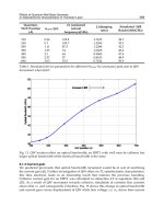
strongly dependent on temperature (P.W.M.Blom et al, 1997) and the fig.8 explains the
variation of current density with respect to applied voltage for different temperature.
Also, the plot of bimolecular recombination constant B for different temperatures (fig.9)
sheds light into the fact that recombination is Langevin type [31] and mathematically it is
expressed in terms of mobility
0
()n
p
r
e
B
(11)
Organic Light Emitting Diodes:
Device Physics and Effect of Ambience on Performance Parameters
11
Fig. 8. Experimental and Calculated (Solid lines) J-V characteristics in hole only (squares)
and double carrier (circle) for different thickness (P.W.M.Blom & Marc J.M,1998).
The enhancement of maximum conversion efficiency is by decreasing non radiative
recombination and by use of electron transport layer which shifts recombination zone away
from metallic cathode.
Fig. 9. Temperature Dependence of Bimolecular Recombination Constant (P.W.M.Blom &
Marc J.M,1998).
Device model based on Poisson’s equation and conservation of charges was more a
traditional presenattion (Y.Kawabe et al,1998) in organic electronic devices. By assuming
that recombination rate is proportional to collision cross section A, electric field, sum of
mobility values of electrons and holes and the product of carrier densities, charge
conservation equation has been rewritten as
,( )
( )() () ()
hex
he h e
dJ
A Exn xn x
dx
(12)
where + and – signs indicate electron and hole currents.
By conservation law of the total current
() () 0
() () () ()
hx ex h h e e
JJeExnxeExnxJ
, (13)
Optoelectronics – Devices and Applications
12
with the boundary conditions given by current injection at both electrodes (Y.Kawabe et
al,1998) .
Besides, current density, relative quantum efficiency was calculated by the model equation
(0) ( ) ( ) (0)
00
hhdede
JJ JJ
JJ
(14)
Here numerical values of the parameters are used to simulate J-V and quantum efficiency
characteristics .Two devices-one with semiconducting polymer (BEH-PPV) and the other
with dye doped polymer (
3
:PVK AlQ
) were fabricated by spin casting techniques and
characterized. The results validate the model for the single layer devices and its suitability
for complex devices is yet to be tested.
The model is having the advantages of incorporating charged traps as shown in equation
below
()
[() () ()]
het
dE x e
nx nx nx
dx q
(15)
where
indicates positive ad negative charges respectively. This sends limelight to the
causes of degradation process in real devices due to the accumulation of electrons in the
vicinity of the cathode. The inferences include low barrier height for low voltage operation,
high mobility for high brightness devices and low electron mobility confines the emission
region near the cathode and should be avoided to prevent electrode quenching.
3. Ambient studies of organic light emitting diodes
The temperature dependence of current density versus bias voltage exhibits interesting
results in organic light emitting diodes. The studies made on four sets of devices namely
Device A: ITO/PEDOT-PSS/MEH-PPV/Al, Device B: ITO/PEDOT-PSS/MEH-
PPV/LiF/Al, Device C: ITO/PEDOT-PSS/Alq3/Al and Device D: ITO/PEDOT-
PSS/Alq3/LiF/Al show the effects of temperature variation in their performance. The
OLEDs were fabricated on ITO coated glass of surface resistivity in the range of tens of
ohms. The standard cleaning procedure (] W. H. Kim et al,2003) in deionized water, acetone
and isopropyl alcohol were carried out. PEDOT:PSS and MEH:PPV were spun cast on ITO
coated glass for polymer devices. For fabricating small molecule based OLEDs, Tris(8-
hydroxyquinolinato) aluminium (Alq3) was vacuum evaporated at 10
-6
torr by physical
vapor deposition. The buffer layer of LiF was also vacuum evaporated in the devices where
such caps were used to enhance the injection of carriers. The metallic cathode was also
vacuum evaporated in all the four sets of devices.The J-V characteristics were plotted by
using a Keithley 2400 Source meter interfaced to a computer. Impedance versus frequency
behavior was studied using Electrochemical workstation IM6 ex from Zahner, Germany. It
also gives the plots of real versus imaginary impedances. The measurements from cryogenic
temperature to room temperature were taken with the help of cryostat. The thickness of the
evaporated as well as spun cast layers and refractive index of PEDOT:PSS film on ITO were
measured by Sopra make Spectroscopic Ellipsometer. The luminance behavior was observed
with the help of a fibre optic spectrometer Avantes.
Organic Light Emitting Diodes:
Device Physics and Effect of Ambience on Performance Parameters
13
3.1 Current density versus bias voltage
The variation of current density with respect to the applied voltage explains the turn on
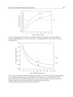
phenomena of the device. Figures 10 and 11 show the J-V characteristics of devices A, B, C
and D respectively at a temperature varying from very low value of 100K to room
temperature. The devices A and B are having MEH:PPV as the emissive layer and their J-V
characteristics are shown in figure 10a and 10b respectively. The devices C and D in which
the emissive material is small molecule Alq3 exhibits a current variation as shown in figure
11a and 11b respectively.
Fig. 10. JV characteristics of Device A and B at different temperatures.
Fig. 11. J-V Characteristics of Device C and D at different temperatures.
The lowest voltage required [26] for the start of tunneling and hence the light emission is the
‘turn on’ voltage. At very small forward voltage, tunneling doest not occur and it begins at
the flat band condition. In fact, ‘flat band voltage’ is the energy gap minus the two energy
offsets. The turn on voltage is a function of the energy levels of the polymer and considered
to be independent of the polymer thickness. The emission from the device starts to occur at a
point where the current starts to increase rapidly when plotted in linear axis. This is the
‘operating voltage’ at which light emission becomes visible to the naked eye and it is a
function of the thickness of the emissive layer.