Crystalline Silicon Properties and Uses Part 7 pot
Bạn đang xem bản rút gọn của tài liệu. Xem và tải ngay bản đầy đủ của tài liệu tại đây (3.53 MB, 25 trang )
Defect Related Luminescence in Silicon Dioxide Network: A Review
139
110 120 130 140 150 160 170 180
1.50
1.55
1.60
1.65
1.70
Si-O-Si bond angle (degree)
a
Si-O bond length (nm)
d
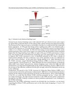
Fig. 2.2 Total energy as a function of Si−O bond length and Si−O−Si bond angle. Contour
lines in units of kJ/mol, [van Santen et al. 1991].
Due to the high Si−O bond energy (4.5 eV), the crystalline quartz is resistant to chemical
weathering (it is only soluble in hydrofluoric acid and in hot alkalis) and to corrosion
[Lamkin et al. 1992, Lide 2004]. It is hard (Mohs' hardness 7), brittle, and has a very high
melting point at around 1710°C [Lide 2004]. Due to its wide energy band gap of about 9 eV,
it is optically transparent and shows low electrical conductivity [Fan et al. 1998].
Generally, a homobond is electrostatically neutral although both Si−Si and O−O bonds may
become positively charged by trapping holes. Irrespective of their electrical charges, defects
can be divided into two classes: diamagnetic and paramagnetic. As a general role, all stable
paramagnetic defects have optical absorption bands associated with them, since they
represent half-occupied energy transitions to the valence band and electron transitions to
the conduction band are both possible. Diamagnetic defects may have absorption bands
associated with electron transitions to the conduction band. The confirmed examples of
diamagnetic defects in a-SiO
2
have electron absorption bands in the ultraviolet or vacuum
ultraviolet spectral regions, implying that the uppermost filled levels of these states lie
below the middle of the 9 eV band gap [Griscom 1977].
A variety of defect structures are known to exist in silica materials and were one of the
major subjects of extensive experimental and theoretical studies [Stevens-Kalceff 2000, Song
et al. 2001, Lu et al. 2002]. Many aspects regarding the nature of the defects and their
correlated properties are still controversial and not yet completely understood. Quite a lot of
defect types have been discussed in the literature and many reproduction models have been
proposed for each one. In this part we will review the main defects in the silica network but
whether any of these models is correct remains an open question of considerable interest.
2.2.1 E´-center
Probably the best known paramagnetic defect in all forms of SiO
2
is the E´-center which was
first detected in late fifties using electron paramagnetic resonance (EPR) spectroscopy
[Weeks 1956, Weeks and Nelson 1960, Griscom et al. 1974, Gobsch et al. 1978]. It is
Crystalline Silicon – Properties and Uses
140
associated with the 5.85 eV absorption band in quartz and silica glass and no associated
emission band has been observed where its nonradiative mechanism has been reported by
some authors [Pacchioni et al. 1998a , Kajihara K. et al. 2003]. From studies of the hyperfine
structure in the EPR spectrum it is known that E´-center can comprise an unpaired electron
in a dangling tetrahedral (sp
3
) orbital of a single silicon atom which is bonded to just three
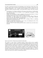
oxygens in the glass network [Griscom 1979a, Isoya et al. 1981]. This generic E´-center is
shown in Fig. 2.3, which is often denoted by ≡Si●, where the three parallel lines represent
three oxygen separate bonds to one silicon atom and the dot denotes the unpaired electron.
O
Si
O
O
.
Fig. 2.3 Generic E´-center. The large atom is silicon, the smaller ones are oxygens
Previous EPR studies on irradiated a-SiO
2
have demonstrated that there are several
distinguishable variants of the E´-center in terms of their g values but in common all have
the structure ≡Si● [Griscom 1990a]. These E´-center variants are also distinguished by virtue
of different annealing kinetics depending on both the character of the irradiation and the
water contents in dry or wet oxidized SiO
2
, as shown in Fig. 2.4 [Griscom et al. 1983,
Griscom 1984, Griscom 1985].
Four main types of E´-centers, labeled E´
α
, E´
β
, E´
γ
and E´
S
have been identified in vitreous
silica depending on their spectroscopic signatures [Skuja 1998]. Several models have been
suggested based on different precursors for each of these defects where some of these types
are associated with hydrogen atoms. Optically stimulated electron emission technique
(OSEE) shows that each one of these types of E´-centers has a distinguishable absorption
band in the range of 5.7 eV [Zatsepin et al. 2000], see Fig. 2.5.
100 200 300 400 500 600 700 800 900 1000
0.01
0.1
1
10
annealing temperature (K)
fractional defect population
g
-ray irradiationx-ray irradiation
peroxy radical
(low-OH silica)
H
o
(high-OH silica)
´E
g
(oxyge dificient
low-OH silica)
´E
g
(low-OH silica)
´E
g
(high-OH silica)
´E
a
(low-OH silica)
´E
b
(high-OH silica)
´E
a
(high-OH silica)
NBOHC
(high-OH silica)
Fig. 2.4 Normalized isochronal anneal curves for radiation-induced defect centers (E´,
NBOHC and peroxy radical) in high-purity silica (low-OH silica: <5 ppm OH and high-OH
silica: 1200 ppm OH), [Griscom 1984].
Defect Related Luminescence in Silicon Dioxide Network: A Review
141
5.0 5.2 5.4 5.6 5.8 6.0 6.2
OSEE intensity x10 (puls/sec)
3
photon energy (eV)
0
1
2
3
4
5
6
7
8
´
E
g
´
E
b
´
E
s
ODC
30 keV
100 keV
Fig. 2.5 OSEE spectra of glassy SiO
2
irradiated by Fe
+
ions of two different energies, 30 and
100 keV, the absorption bands of E´
β
, E´
γ
and E´
S
-centers are detected, besides a very weak
absorption band associated with oxygen deficient centers (ODC), [Zatsepin et al. 2000].
It was inferred that the E´
α
variant in silica initially observed by Griscom [Griscom 1984], is
a defect which tends to anneal in times on the order of minutes up to hours above 100 K. It
was suggested that this center is created by a radiolytic process which moves an oxygen
atom from an undisturbed network site ≡Si−O−Si≡) into a neighboring position which must
be chemically bonded, since insufficient energy can be transferred from an X-ray generated
compton electron to result in a net breakage of bonds [Uchino et al. 2001]. Fig. 2.6 illustrates
one of the conceivable ways in which such a process could come about. The oxygen-oxygen
(peroxyl ≡Si−O−O) bond suggested to be formed in Fig. 2.6 should be a relatively stable
entity according to recent theoretical calculations [Griscom 1979a]. Still, less exotic
mechanisms for E´
α
production, not inconsistent with the data, might be the momentary
rupture of strained oxygen bonds ≡Si···O−Si≡). Here ●O−Si≡ is the notation for the non-
bridging oxygen hole center (NBOHC), and is in fact seen by electron spin resonance (ESP)
in X-ray irradiated silicas in numbers comparable to the E´
α
-center.
O
O
Si
O
O
O
Si
O
O
idel network site + peroxy radical + e strained bond + NBOHCEE
´´
-
O
O
Si
O
e
-
O
O
Si
O
O
O
Si
O
O
O
O
Si
O
O
O
Si
O
O
O
Si
O
O
O
O
a
a
Fig. 2.6 Schematic models for the E´
α
-center in pure a-SiO
2
, the arrow denotes the unpaired
spin and dashed balloons represent their orbital.
E´
β
in silica network (E´
2
in quartz) features a proton trapped in the oxygen vacancy and the
silicon atom containing the unpaired spin relaxed outwards [Griscom 1991, Weeks 1963], i.e.
Crystalline Silicon – Properties and Uses
142
the interaction of the unpaired spin associated with a long-bond silicon with the hydrogen
atom is weak enough to not saturate each other. Two possible formation reactions of E´
β
are
shown in Fig. 2.7.
O
O
Si
O
O
O
Si
O
O
H
O
O
Si
O
O
Si
O
O
O
O
Si
O
H
O
Si
O
O
H
O
O
Si
O
H
O
Si
O
O
O
idel network site + H or + interstitial O unrelaxed oxygen vacancy+ H or
o o
E E E´ E´
´´
b
2
b
2
Fig. 2.7 Schematic models for the E´
β
-center in pure a-SiO
2
. The arrow denotes the unpaired
spin and dashed balloons represent their orbital. The E´
β
-center is considered to be the
closest analog for E´
2
-center in quartz.
E´
γ
–center is the closest analog of the E´
1
-center in α-quartz [Griscom 1980, Boero et al. 1997].
According to current theoretical calculations [Feigl et al. 1974, Yip and Fowler 1975,
Mysovsky et al. 2004], E´
γ
is suggested to consist of a positively charged single oxygen
vacancy composed of a nearly planar ≡Si
+
unit and a singly occupied dangling bond ≡Si●,
namely, ≡Si+ ●Si≡ [Uchino et al. 2000b, Agnello et al. 2002]. An unrelaxed oxygen
monovacancy (≡Si···Si≡) or an unperturbed SiO
2
fragment (≡Si−O−Si≡) is assumed to be the
precursor of this defect as shown in Fig. 2.8. There is no indication that hydrogen is involved
in this defect [Feigl et al. 1974]. E´
γ
is stable for years at room temperature [Griscom 1984].
O
O
Si
O
O
O
Si
O
O
O
O
Si
O
O
Si
O
O
O
O
Si
O
O
Si
O
O
O
+
O
O
Si
O
O
Si
O
O
+
e
-
-
idel network site or + interstitial O unrelaxed oxygen vacancy or + eEE EE
´´ ´´
-
1
g
1
g
Fig. 2.8 Schematic models for the E´
γ
-center in pure α-SiO
2
. The arrow denotes the unpaired
spin and dashed balloons represent their orbital. The E´
γ
-center is considered to be the
closest analog for E´
1
-center in quartz.
Relaxing of the Si atom with the unpaired spin towards oxygen vacancy results in the E´
4
-
center. It is in fact the most reliably characterized of these defects depending on the
experimental and theoretical analysis [Isoya et al. 1981]. E´
4
-center consists of a hydrogen
substituting for an oxygen atom in α-quartz [Mysovsky et al. 2004]. This center, Fig. 2.9, is
observed in crystalline silicon dioxide (α-quartz) but there is no evidence of existence of E´
4
-
center in silica glass [Griscom and Friebele 1986]. Some other authors [Rudra et al. 1985,
Majid and Miyagawa 1993, Snyder and Fowler 1993] suggested that the E´
2
and E´
4
are in
fact the same defect, but with long-bond silicon relaxed through the plane of its three
oxygen neighbors such that the unpaired spin points away from the vacancy. But this
configuration is predicted to be slightly lower in energy than the E´
4
configuration. In
surface center studies, several variants of surface E´-centers were found [Bobyshev and
Radtsig 1988]. Two of them are depicted in Fig. 2.10, E´
S
(1) which seems like the normal E´-
center but with a constant isotropic hyperfine splitting, and the second is E´
S
(2) which has a
dangling silicon bond with a neighboring hydroxyl (OH) group [Skuja 1998].
Defect Related Luminescence in Silicon Dioxide Network: A Review
143
O
O
Si
O
O
O
Si
O
O
H
O
O
Si
O
O
O
O
Si
O
H
idel network site + H + interstitial O
o
E
´
4
Fig. 2.9 Schematic model for E´
4
-center in crystalline SiO
2
. The arrow denotes the unpaired
spin which interacts with a hydrogen atom to relax the oxygen vacancy by forming Si−Si
bond.
E (1)´ E (2)´
O
O
Si
O
H
O
O
Si
O
SS
Fig. 2.10 Schematic models for surface E´-center (E´
S
) in pure a-SiO
2
. The arrow denotes the
unpaired spin and dashed balloons present their orbital. Hydrogen saturates the dangling
oxygen bond
2.2.2 Oxygen-deficiency center (ODC)
It should be mentioned first that all E´-center types are also considered as oxygen deficiency
centers but in this subsection a review of a different (non-paramagnetic) kind of oxygen
deficiency center will be given. This defect center is entitled simply by a neutral oxygen
vacancy which is often denoted ODC and indicated generally as ≡Si−Si≡.
O
O
Si
O
O
Si
O
O
+
relaxed neutral unrelaxed neutral neutral oxygen twofold Si fully bonded
oxygen vacancy ODC(I) oxygen vacancy ODC(II) vacancy ODC(I) ODC(II) idel network site
O
O
Si
O
O
Si
O
O
O
Si
O
O
Si
O
O
O
O
O
O
Si
Si
O
O
O
Si
O
O
O
Si
O
Si
O
O
Fig. 2.11 Schematic illustration of the transformation between ODC(I) and ODC(II)
visualizing two possible models for the ODC(II), the unrelaxed oxygen vacancy and the
twofold coordinated silicon.
It is diamagnetic and can be directly investigated by photoluminescence (PL) or
cathodoluminescence (CL) spectroscopy. The literature mostly describes two models for the
ODCs: neutral oxygen vacancy ODC(I) and the twofold coordinated silicon ODC(II)
denoted as =Si●●. The ODC(I) represents one of the essential defects in all silicon dioxide
modifications in a form of simple oxygen vacancies; here two Si atoms could relax and make
a silicon silicon bonding (relaxed oxygen vacancy ≡Si−Si≡) or stay in unstable interaction
condition and form an unrelaxed oxygen vacancy (≡Si···Si≡) which each one of them could
be a precursor for the other under some undeclared circumstances, see Fig. 2.11, and both
are considered as a key role in many defect-type generations and transformations in the
silica matrix, as shown in Figs. 2.7 and 2.8. The 7.6 eV absorption band in irradiated and as
grown a-SiO
2
has been ascribed to the neutral oxygen vacancy ODC(I) [Imai et. al 1988,
Crystalline Silicon – Properties and Uses
144
Hosono et al. 1991]. The ODC(I) can also be converted to ≡Si−H groups in thermal reaction
with hydrogen molecules according to the visualized reaction shown in Fig. 2.12.
ODC(I) + H Si O group (silanol)
O
O
Si
O
O
Si
O
O
O
O
Si
O
O
H
H
O
O
Si
O
O
H
H
Fig. 2.12 Schematic illustration of the ODC(I) conversion to silanol groups in thermal
reaction with hydrogen molecules.
In addition, two photoluminescence (PL) bands, 4.4 eV (decay constant τ=4 ns) and 2.7 eV
(decay constant τ=10.4 ms) have been observed under excitation of the 5 eV, 6.9 eV or 7.6 eV
bands, indicating the interaction of ODC(II) with ODC(I) [Nishikawa et al. 1994, Seol et al.
1996]. Based on their lifetimes, the 4.4 eV and 2.7 eV bands have been ascribed to singlet-
singlet (S
1
→S
o
) and triplet-singlet (T
1
→S
o
) transitions at the site of oxygen-deficient type
defects, respectively [Skuja 1998]. The interconversion between the ODC(I) and ODC(II) in an
energy diagram is given in Fig. 2.13. The origin of ODC(II) associated with the optical
absorption band at ~5 eV is one of the most controversial issues in the defect research field of
a-SiO2 [Skuja et al. 1984, Griscom 1991, Skuja 1992a, Skuja 1998]. The first model hypothesis
suggested for ODC(II) was a neutral diamagnetic oxygen vacancy [Arnold 1973], later two
other models have been proposed for ODC(II): twofold coordinated silicon [Skuja et al. 1984,
Skuja 1992a] and the unrelaxed oxygen vacancy [Imai et al. 1988] as shown in Fig. 2.11.
The oxygen vacancy model was further supported by the finding that two-photon
photobleaching of SiODC(II) by KrF laser (ħω=5 eV) generates E´-centers [Imai et al. 1988].
But the origin of the ODC(II) is still a matter of controversy.
ODC(I) ODC(II) ODC(I)
S
o
S
1
S
2
7.6 eV
5eV
6.9 eV
S
o
T
1
T
2
3.15 eV
2.2 eV
4.4 eV
t
=4.0 ns
2.7 eV
t
=10.4 ms
1
2
3
4
5
6
7
8
0
energy (eV)
DE
act
=0.13 eV
S
o
S
1
Fig. 2.13 Diagram of the energy levels proposed for the optical transitions at the site of two
oxygen-deficient centers: ODC(I) and ODC(II). Transformation between the two states is
assumed by the excitation at 7.6 eV. Solid and dotted arrows represent radiative and non-
radiative electronic transitions, respectively. ΔE
act
is the thermal activation energy for
singlet-triplet conversion, τ are the radiative decay times, [Skuja 1998 and Nishikawa 2001].
Defect Related Luminescence in Silicon Dioxide Network: A Review
145
2.2.3 The non-bridging oxygen hole center (NBOHC)
This center can be visualized as the oxygen part of a broken bond (Figs. 2.6 and 2.15). It is
electrically neutral and paramagnetic and represents the simplest elementary oxygen-
related intrinsic defect in silica. It is well characterized both by EPR and by optical
spectroscopies like photoluminescence (PL) and cathodeluminescence (CL).
The main optical characteristics of NBOHC are shown in Fig. 2.14, it has an absorption band
at 4.8 eV with FWHM=1.07 eV, oscillator strength f=0.05; an asymmetric absorption band at
1.97 eV, FWHM=0.17 eV, f=1.5×10
-4
; a photoluminescence band excited in these two
absorption bands, at 1.91 eV , FWHM=0.17 eV, decay constant around 20 μs. Out of these
three characteristics, the most unique fingerprint of this center is the 1.9 eV luminescent
band in the red region of the visible light spectra.
It has been postulated that the NBOHC arises when hydrogen atoms are liberated
radiolytically from one member of a pair of OH groups in wet silica (high OH group)
according to Fig.2.15 [Stapelbrok et al. 1979].
photon energy (eV)
optical absorption (cm )
-1
1234567
0
1
2
3
4
5
photoluminescence band at 1.9eV
life time 20 sm
photoluminescence band at 1.9eV
life
time 20 sm
optical absorption/excitation
band at 1.97eV
optical absorption/excitation
band at 4.8eV, FWHM 1.07eV
.
induced optical absorption
in -irradated wet SiOg
2
g
x 200
.
Fig. 2.14 Optical absorption and luminescence spectra of γ-irradiated wet silica illustrating
the main optical properties of NBOHC: the absorption/excitation bands at 4.8 eV and 1.97
eV, and the photoluminescence band at 1.9 eV, [Pacchioni et al. 2000].
silanol group NBOHC + hydrogen
O
O
Si
O
O
H
H
O
O
Si
O
O
O
Si
O
Si
O
O
H
O
O
Si
O
O
H
Fig. 2.15 A model of atomic structure of the non-bridging oxygen hole center (NBOHC)
showing the possible generating processes of NBOHC in wet silica.
Crystalline Silicon – Properties and Uses
146
Conduction BandConduction Band
E
v
1.9 eV2.0 eV
1.97 eV1.97 eV
2.10 eV
E
g
=9 eV
Si
O
SiO
H
4.8 eV
SiO
Si
O
energy transfer
Valence BandValence Band
E
c
Fig. 2.16 Energy band diagram of different NBOHC energy states, [Munekuni et al. 1990].
However this reaction is not the only way of creating NBOHC. Oxygen dangling bonds may
be created as well in wet and in dry silica (negligible amounts of OH groups) by rupturing
of the strained Si−O bonds (≡Si···O−Si≡) in the silica network (Fig. 2.6). Particularly there are
no spectroscopic distinctions which have been established between the centers formed by
these two precursors, but on the other hand some authors [Munekuni et al. 1990] proposed
some differences in their emission energies, see Fig. 2.16.
If softer irradiation (X-ray) was used, the centers were created only in groups of Si−O−R (R:
alkali ion). This behavior provides evidence that the centers are created in reactions similar
to that visualized in Fig. 2.15, and they were attributed to NBOHC [Skuja 1994a, Skuja et al.
2006]. On silica surfaces, the same red luminescence band can be created by adding O atoms
to surface E´-centers [Streletsky et al. 1982]. Another generic oxygen hole center is the self-
trapped hole (STH), which exists in two different variants. STH
1
comprises a hole trapped
on a normal bridging oxygen in the network (≡Si−°O−Si≡), while the STH
2
is suggested to
consist of a hole delocalized over two bridging oxygens [Griscom 1991, Griscom 2000].
2.2.4 Peroxy bridge (POL)
In oxygen-excess silica, some of the excess oxygen is expected to form "wrong" oxygen-
oxygen bonds, called peroxy bridges or peroxy linkages (≡Si−O−O−Si≡). Calculations of
atomic oxygen diffusion in SiO
2
suggested that POL structure is the lowest energy
configuration for an oxygen interstitial [O`Reilly and Robertson 1983]. However, a definitive
spectroscopic confirmation of their presence in silica is still absent. The experimental
evidence is only indirect, but it is thought to be responsible for the exclusive (without the
accompanying Si−H groups) generation of Si−OH groups during H
2
treatment of oxygen
rich silica [Imai et al. 1987], as shown in Fig. 2.17. This reaction is accompanied by an
increase of VUV optical absorption for hν>7 eV indicating that the POL could possibly
absorb in this region. POL was initially suggested to be the main precursor of peroxy radical
defects, Fig. 2.18, as we will show in the following subsection [Friebele et al. 1979]. The
calculation put the energy of the POL absorption band at around 6.4-6.8 eV with a small
oscillator strength, f=2×10
-4
[Pacchioni and Ierano 1998b], such absorption would be hard to
detect against the background of other bands in vacuum UV.
2.2.5 Peroxy radical (POR)
The Peroxy radical (POR) in silica is a paramagnetic defect with a hole delocalized over anti-
bonding π-type orbitals of the O−O bond in the structure illustrated in Figs. 2.17 and 2.18.
EPR spectroscopy shows that the POR is the best characterized oxygen excess defect in silica
Defect Related Luminescence in Silicon Dioxide Network: A Review
147
O
O
Si
O
peroxy bridge + hydrogen silanol group peroxy bridge peroxy radical + e
-
e
-
O
Si
O
Si
O
O
O
O
O
Si
O
O
H
H
O
O
Si
O
O
H
O
O
Si
O
O
O
O
Si
O
O
O
Si
O
O
O
H
O
O
Si
O
O
Fig. 2.17 Models presenting the suggested atomic structure of a peroxy bridge (POL) and its
role in producing other possible defects in silica matrix.
O
Si
O
Si
O
O
Si
O
O
+
-center + oxygen peroxy radical NBOHC + oxygen peroxy radicalE
´
O
O
O
Si
O
Si
O
O
O
Si
O
O
O
+
O
Si
O
Si
O
O
Si
O
O
O
O
O
Si
O
Si
O
O
O
O
Si
O
O
Fig. 2.18 Models presenting some possible generation modes for the peroxy radical (POR)
structure in the silica matrix.
[Griscom 1991, Friebele et al. 1979]. However, the optical properties of POR in bulk silica are
not accurately known. Good correlations between the isochronal annealing curves of EPR
signals of POR and of the optical absorption band at 7.7 eV were reported in γ-irradiated
dry silica [Stapelbroek et al. 1979]. The optical absorption spectrum observed for peroxy
radicals on the surface of SiO
2
by the diffuse reflectance technique in the region around
5.4 eV with FWHM 1.3 eV and oscillator strength f≈0.067 was calculated [Bobyshev and
Radtsig 1988].
2.2.6 The self-trapped exciton (STE)
The electronic excitation of solids produces mainly electrons, holes and excitons.
Transient (short living) defects can be created through the combination of the electronic
excitation energy of electron-hole pairs and electron-phonon interaction. The conversion
of excitation to defects is initiated by self-trapping of excitons, by the trapping of electrons
by self-trapped holes or by the consecutive trapping of an electron and hole by a defect.
These transient defects can produce either radiative or non-radiative electronic transition,
while non-luminescent transient defects disappear by recombination of defect pairs. Self-
trapping is a widespread phenomenon in insulators [Hayes and Stoneham 1985, Song and
Williams 1993].
The existence of the self-trapped excitons in crystalline SiO
2
is supported by experimental
measurements of the optically detected magnetic resonance and transient volume change
[Itoh et al. 1988]. The luminescence bands between 2 and 3 eV in the silica spectrum have
been ascribed to the STE. Some authors suggested that the STE is the source of the
characteristic blue luminescence in crystalline SiO
2
, but it has been observed that this
luminescence band is removed in quartz by intense electron irradiation (15 keV) at room
temperature due to the electron hole recombination as shown in Fig. 2.19 [Griscom 1979b,
Trukhin 1978, Trukhin 1980, Barfels 2001]. Almost the same luminescence band can be
detected in the emission spectra of amorphous SiO
2
but with much lower intensities than the
Crystalline Silicon – Properties and Uses
148
other characteristic bands. STE perturbed by small distortions due to a structural defect give
emissions in the same energy range. For example, Ge implanted quartz exhibits a
luminescence band at 2.5 eV close to 2.8 eV in non-implanted quartz [Hayes and Jenkin
1988]. The excitation spectra for STE luminescence in α-quartz show a peak at 8.7 eV, which
is ascribed to the first exciton peak. The absorption edge has been determined as 9.3 eV [Itoh
et al. 1989], so the exciton binding energy is about 0.6 eV for α-quartz [Bosio and Czaja
1993]. The large energy difference between the band edge absorption (about 9 eV) and
luminescence (2.8 eV) points to strong electron-photon coupling. The optical absorption
spectra and the excitation spectra for fused silica are similar to those of α-quartz but exhibit
modifications due to the amorphous structure [Trukhin 1992].
200 300 400 500 600 700 800
0
2
4
6
8
10
12
290 K
80 K
G
UV
B
R
Quartz
6 5 4 3 2.5 2 1.8 1.6
energy (eV)
wavelength (nm)
IR
290 K
80 K
G
UV
B
R
Stishovite
6 5 4 3 2.5 2 1.8 1.6
energy (eV)
wavelength (nm)
200 300 400 500 600 700 800
CL-intensity x10 (a.u.)
3
V
V
Fig. 2.19 CL-spectra of some crystalline SiO
2
(Quartz and Stishovite) at 290 K and 80 K,
[Barfels 2001].
Meanwhile, several models have been proposed implying to clarify the STE. One of the first
models considering that an oxygen atom will removed to a peroxy bridge position [Griscom
1979a, Griscom 1979b] and other models are based on the proposition that a threefold
coordinated silicon explains the transient absorption at 5.2 eV (E´-center) [Trukhin 1992,
Trukhin 1994], see Fig.2.20. All of these suggested models are based on the idea that the
silicon-oxygen bond (Si−O) gets ruptured and forms an oxygen-oxygen bond (−O−O−)
based on the fact that different local structures of the SiO
2
network provide different
distances for oxygen-oxygen bonding. Each oxygen atom bonded to two silicon atoms by
two types of Si−O bond, one by long bond ≈1.612 Å and another by short bond ≈1.607 Å, as
shown in Fig. 2.20 by dashed and solid bond connections [Hayes et al. 1984, Trukhin 1994].
These models explain different STE luminescence properties of different structures.
idel network site peroxy bridge + oxygen vacancy -center + O O bondE´
O
Si
O
O
O
O
Si
O
Si
O
O
Si
O
O
O
Si
O
Si
O
Si
O
O
O
Si
O
O
O
O
O
Si
O
O
O
Si
O
Si
O
Si
O
O
O
Si
O
O
O
O
Fig. 2.20 Models of self-trapped exciton (STE) showing a creation of oxygen vacancy, E´-
center and peroxy bridge due to the decay of a STE associated with an excited Si−O bond in
crystalline SiO
2
.
Defect Related Luminescence in Silicon Dioxide Network: A Review
149
2.2.7 Interstitial oxygen
Mostly all variants of manufactured high-purity dry SiO
2
contain natural interstitial oxygen
atoms and an additional amount can be generated by ejecting oxygen atoms from their
normal sites in the SiO
2
network during the irradiation. Another important point that has to
be considered is the molecular oxygen. Principally O
2
molecules can be formed
in irradiation processes from the already present oxygen atoms [Morimoto et al. 1992].
The first spectroscopic observation of O
2
molecules in silica was performed by Raman
spectroscopy in optical fibers [Carvalho et al. 1985]. O
2
was detected by O−O stretching
vibration at wavenumber 1549 cm
-1
. Using this method the O
2
molecule concentration
is found to be in the range of 10
14
-10
18
molecules per cm
3
in dry silicon dioxide [Skuja
et al. 1998a].
In gas phase, oxygen molecules (O
2
) dissolved to two atomic oxygen (2O) for hν>5.1 eV
(λ<242 nm); the same can be expected to occur in silica glass following the photolytic
reaction shown in Fig. 2.21. The atomic oxygens appearing as a result of this reaction might
be expected to be relatively mobile in silica even at room temperature; then they interact
with other oxygen molecules to form ozone (O
3
) just as it occurs in the earth's atmosphere
[Baulch et al. 1980, Finlayson-Pitts and Pitts 1986]. There are indications that the atomic
oxygen becomes mobile at around 400 °C as detected by formation of the interstitial oxygen
molecules at this temperature [Skuja et al. 2002, Kajihara et al. 2004]. Depending on the
quantum yield for the gas-phase reaction of ozone dissociation, it is believed that O
3
molecules are responsible for both the 4.8 eV absorption and 1.9 eV luminescence in certain
oxygen-rich silicas [Awazu and Kawazoe 1990, Griscom 1991, Skuja et al. 1995], which
usually are attributed to the NBOHC by many authors [Kajihara et al. 2001, Cannas and
Gelardi 2004, Bakos et al. 2004b]. The 1.9 eV luminescence band shifts between 1.8 and 2 eV
depending on the excitation wavelength within the 2 eV absorption band [Skuja et al. 1995].
Other bands of possibly related origin have been observed in the 2.0-2.5 eV regions
[Munekuni et al. 1990, Skuja 1994a]. O
¯
2
and O
¯
3
can be other candidates for the 1.8 eV band
but the only truly unanimously agreed point is that the 1.8 eV luminescence band is related
to excess oxygen in silica [Skuja et al. 1995].
Although the amount of interstitial O, O
2
and O
3
can be negligible in comparison with the
whole oxygen content in a silica network, the presence of these interstitial atoms or
fragments has to be considered when analyzing a large amount of accumulated defects in
the silica matrix.
O
Si
O
Si
O
O
O
Si
O
O
O in the network O atoms in the network O in the network O in the network
2 23
O
Si
O
Si
O
O
O
Si
O
O
hn
>5.1eV
O
O
O
Si
O
Si
O
O
O
Si
O
O
O
Si
O
Si
O
O
O
Si
O
O
O
O
O
O
O
O
O O
hn
>3.9eV
Fig. 2.21 Main interstitial atomic and molecular oxygen as well as ozone model in SiO
2
.
2.2.8 Hydrogen-related defects and the state of water in SiO
2
Hydrogen in the form of steam has been used intentionally during thermal oxidation to
increase oxidation rates. Very often it is also incorporated unintentionally into SiO
2
layers.
Hydrogen is proposed to passivate the silicon or oxygen dangling bonds in SiO
2
network
[Cartier et al. 1993, Fair 1997]. This passivation also decreases the number of non-bridging
Crystalline Silicon – Properties and Uses
150
oxygens which in turn reduces the viscosity of the silica layers substantially [Rafferty 1989].
Some authors considered hydrogen to be an intrinsic defect since it is commonly found in
silicon dioxide. Hydrogen and water are ubiquitous impurities in SiO
2
. The energy levels of
silanol (≡Si−O−H) and hydride (≡Si−H) groups have been calculated by tight-binding
calculation [Robertson 1988]. The hydride groups seem to produce a filled s state just below
the valence band (VB) and an empty σ
*
state in the gap just below the conduction band (CB).
This group is probably both an electron and a hole trap.
Hydride groups are expected in thermally grown silica, particularly near the interface due
to the interaction of interstitial H
2
molecules with Si−O−Si bridges. The H
2
is a byproduct of
the fast oxidation of Si by any ambient water.
O
Si
O
Si
O
O
O
Si
O
O
idel network site + H O bond stetching process sianol group
2
O
H
H
O
Si
O
Si
O
O
O
Si
O
O
O
H
H
O
Si
O
Si
O
O
O
Si
O
O
O
H
H
stretching direction
stretching direction
Fig. 2.22 A model of the structural state of water in SiO
2
network and its transformation to
silanol groups, [Brunner et al. 1961, Bakos et al. 2004a].
O
O
Si
O
O
Si
O
Si
O
O
O
Si
O
O
O
O
H
H
O
O
Si
H
H
O
4H atoms substitution of Si + O generation of H O molecule
2
O
O
O
Si
O
Si
O
O
O
Si
O
O
H
H
O
O
Si
H
O
O
O
O
Si
O
O
H
Fig. 2.23 A model of the structural state of water in SiO
2
lattice and its formation, [Nuttall
and Weil 1980, McLaren et al. 1983].
It is proposed that water can be incorporated into the SiO
2
lattice according to the reaction
illustrated in Fig. 2.22 [Brunner et al. 1961, Bakos et al. 2004a]. This is a preferred stress-
induced mechanism and referred to "as hydrolytic weakening" [Griggs and Blacic 1965,
Griggs 1967]. Calculations of total energy indicate that this reaction which uses an energy
of ~0.1 eV is spontaneous for a Si−O bond stretched beyond 4% of its normal bond length
[Heggie 1992]. It has also been suggested that the solubility of water in the quartz lattice
depends on the aluminum content [Kronenberg et al. 1986].
Another possible configuration shown in Fig. 2.23, assumes that hydrogen is incorporated in
the quartz structure by means of (4H)Si defects where 4H
+
substitutes for Si4
+
[Nuttall and
Weil 1980 , McLaren et al. 1983].
3. Fundamental of cathodoluminescence
3.1 Electron beam interaction with matter
When an electron hits a solid surface, it penetrates into the microstructure of the solid and
interacts with its atoms. The resulting effects allow the extraction of analytical information
Defect Related Luminescence in Silicon Dioxide Network: A Review
151
Incident electron beam
Secondary electrons (SE)
topographical information
a
Backscattered electrons (BE)
tomic number and phase differences
Characteristic X-ray (EDX)
thickness composition information
Continuum X-ray (Bremsstrahlung)
insulator charging
100
200
300
400
500
Cathodoluminescence (CL)
electrric states information
Specimen surface
Auger electrons (AE)
surface constituents
0
Excitation volume
Specimen ( SiO )
2
Substrate ( Si )
Interface ( Si / SiO )
2
thickness (nm)
d
Sample current (SC)
Electron beam induced conductivity (EBIC)
Fig. 3.1 Schematic representation of processes resulting from electron bombardment
(modified after Reimer 1998). Note that the emissions come from different depths, e.g. CL
and X-rays are emitted from deeper section levels than the secondary electrons.
on various properties of the material. The elementary interaction process involves collision
of the electron with an atom, either with the positive atomic nucleus or with the electrons.
Since the colliding particles are charged, the interaction is governed essentially by
electrostatic Coulomb force. In an electron-nucleus collision, the atomic nucleus hardly
changes its position since it is much heavier than the electron. The electron is therefore
deflected at the nucleus without significant energy loss (elastic scattering). If the electron
collides with the electrons of the atomic shells, then energy is transferred due to the equal
masses of the colliding particles (inelastic interaction). Both scattering processes operate
simultaneously side by side and provide a wide variety of useful signals. As a consequence
of these different scattering events, an electron probe which originally was sharply focused
in vacuum spreads over a greater volume after penetrating the solid. The shape and size of
this scattering volume depends upon the material as well as the energy and angle of
incidence of the probe electrons [Reimer 1998].
The elastic interactions between electrons and atoms or between electrons and the crystal
lattice gives rise to a number of effects; the emission of secondary electrons (SE), back-
scattering of electrons (BE), Auger electrons (AE), characteristic X-ray (EDX) and
cathodoluminescence emission (CL) but mainly most of the electron beam's energy will be
absorbed (sample current) and converted into heat (phonons) [Ozawa 1990]. AEs and more
generally SEs can only escape from the first few nanometers of the surface. This means that
these signals originate from the top of the interaction volume, the lateral size of which is
determined by the electron probe size which in turn defines the spatial resolution in AES
and SEM. Backscattered electrons are higher in energy and can escape from deeper areas
below the surface where the interaction volume is wider laterally, this results in a degraded
image resolution for backscattered electron imaging in the SEM relative to that of secondary
electron imaging [Reimer 1998]. Analyzing these signals may provide valuable information
about the surface and atomic structure of the investigated substance. Two of these signals
Crystalline Silicon – Properties and Uses
152
interatomic distance
conduction band
valence band
CL
X-ray
energy
++++
Fig. 3.2 Energy band diagram of one-dimensional lattice, [Yacobi and Holt 1990].
were among our main interest in this study, CL for luminescence defects investigation and
EDX used for the atomic element component analysis. Fig. 3.1 illustrates schematically these
effects and their major common applications.
The term cathodoluminescence (CL) designates the luminescence induced by energetic
electron bombardment. Cathodoluminescence is excited from the region near the surface of
the specimen and up to deeper than X-rays excitation volume, see Fig. 3.1. Therefore, the
energy of the incident electron beam can be rather low (1-5 keV) to excite significant
cathodoluminescence signals of use for the various applications. The CL signal is formed by
detecting photons of the ultraviolet (UV), visible and near-infrared (IR) regions of
the spectrum. These photons are emitted as the result of electronic transitions between
the conduction and valence bands in semiconductors, and transitions between energy
levels lying in the band gap of materials with wide band gap (insulators), Fig. 3.2. Many
useful signals in these cases are due to transitions that involve impurities and a variety
of defects.
X-ray spectrometry is based on the emission of X-rays from the atoms of a solid when struck
by particles or waves of sufficiently high energy (electron beam in our case), followed by the
relaxation of the atoms to the ground state after ionization. The X-ray spectrum produced by
electron excitation consists of two parts, a continuous spectrum of deceleration radiation,
known as "bremsstrahlung", and a line spectrum of the characteristic radiation.
Characteristic X-rays will only be excited in the volume in which the electron energy
exceeds the ionization energy of the inner shell involved. The general concept of X-ray
emission-region and emission-process are shown in Figs. 3.1 and 3.2. The electron beam
energy is typically in the range 10-20 keV and the energy of the X-rays emitted depends on
the material under examination. The X-rays are generated in a region about 1-4 μm in depth,
thus EDX is not a surface science technique, but it is a method used for providing sample
composition information besides charging properties of insulators. Both CL and EDX
techniques are commonly used in combination with a scanning electron microscope (SEM).
3.2 Process of luminescence excitation
Luminescence is produced by electron transitions between different energy levels. It may be
produced by a band-band transition, transitions from band to localized state, or even
between two localized states in a defect molecule, see Figs. 3.3 and 3.4. Luminescence is
considered to form mainly in three steps. First, absorption of the excitation energy and
stimulation of the atoms into an excited state, then transformation and transfer of the
Defect Related Luminescence in Silicon Dioxide Network: A Review
153
Forbidden gap
E
g
LuminescenceLuminescence
LuminescenceLuminescence
LuminescenceLuminescence
LuminescenceLuminescence
Conduction BandConduction Band
excitation
energy
(a) (b) (c) (d) (e) (f)
LuminescenceLuminescence
acceptor E
a
_
trap E
d
LuminescenceLuminescence
E
c
E
v
+
Valence BandValence Band
Fig. 3.3 Mechanisms of cathodoluminescence due to recombination processes in
semiconductors or insulators: (a) recombination by direct band-to-band transition leads to
intrinsic cathodoluminescence ; (b-e) recombination via localized states in the forbidden gap
results in extrinsic cathodoluminescence; (f) excitation and recombination within the defect
energy levels. E
a
=accepter level, E
d
=donor level, modified after Krbetschek et al. 1997.
excitation energy, and finally emission of light and relaxation to a non-excited state [Yacobi
and Holt 1990]. The first two steps mainly depend on the mode of excitation, whereas the
third step depends on the character of specific luminescence centers.
In crystals, complex interaction between atoms leads to the broadening of the energy levels
into bands. In insulators like silica, a broad gap, called the forbidden gap, exists between the
valence band and the conduction band. A precondition for cathodoluminescence is the
existence of activators (impurity ions, lattice defects), which cause and occupy discrete
energy levels in this forbidden zone. Luminescence centers can be differentiated by their
energy position within the forbidden gap and divided into electron traps near the
conduction band (donor level) and recombination sites in the vicinity of the valence band
(acceptor level).
CL involves electron radiation induced excitation of an electron from the ground state to
an excited state. Recombination of an electron from the conduction band with a hole in the
valence band is possible in variety of ways: it may take place by a band-to-band transition
or step by step via localized energy states within the forbidden gap. In a band-to-band
transition shown in Fig. 3.3a, light is emitted with a photon energy hν=E
g
=E
c
-E
v
; this type
of CL is called intrinsic luminescence. Intrinsic CL is only likely to occur in
semiconductors (GaAs and ZnS) in which recombination can take place directly, i.e
without changes in momentum. In indirect semiconductors (Si, Ge, and GaP) the special
band structure requires a photon to take part in the recombination process so that
momentum is conserved.
The extrinsic CL is a recombination that takes place via localized energy states within the
forbidden gap. Excitation results in the trapping of an electron or in the recombination with
a luminescent or a non-luminescent center (Fig. 3.3b). In the case of a luminescent transition,
a photon is emitted. If the atom or the ion is placed in a crystal lattice, non-luminescent
transitions are possible due to absorption or emission of lattice vibrations. A trapped
Crystalline Silicon – Properties and Uses
154
electron can be excited again, transits into the conduction band and may recombine with an
activator element level resulting in emission of a photon (Fig. 3.3c), or a trapped electron
may relax to the valence band and emit a photon (Fig. 3.7d). In the case of a small energy
difference between electron trap and activator level, a direct luminescent transition of the
electron to the recombination centre is possible (Fig. 3.3e). A More complex process is the
excitation of several energy states lying deeper inside the forbidden gap and the subsequent
relaxation and luminescence emission of a single activator is also possible (Fig. 3.3f). Such
states can be due to point defects (impurities or lattice defects) and act as traps for electrons
or holes. The variety of possible transitions and the thermally induced broadening of the
energy states make the CL spectra very difficult to interpret.
Fig. 3.4 Possible processes of excitation of a luminescence center explained in depending on
configuration coordinate diagram assuming (a) radiative transition , (b) non-radiative
transition , and (c) thermally assisted excitation into the conduction band, [Krbetschek et al.
1997].
The process of excitation and emission of an individual luminescence center can be
described using a configuration coordinate diagram. It shows the potential energy curve of
the absorbing center as a function of the relative distance (r) of the nucleus to the
equilibrium position (electron in the ground state). Fig. 3.4 shows excitation of a defect
atom/molecule from the ground state (Q
i
) to excited state (Q
f
) combined with radiative (Fig.
3.4a) and nonradiative (Fig. 3.4b) relaxation. As a particular case of excitation, thermally
assisted excitation (Fig. 3.4c) into the conduction band and the relationship between the
configurational coordinate and the band model are also shown.
In optical absorption (E
a
) the center is promoted from the ground state to a higher vibration
level of the excited state. After relaxation (R) to the zero vibration level of the excited state
the electron returns with luminescence emission (E
e
) or via a nonradiative transition with
the emission of photons (ρ) and relaxes to the zero vibrational level (R
o
). Since the electron
transitions are faster than lattice relaxation, the absorption occurs adiabatically as a vertical
transition (the Frank-Condon principle). The energy difference between absorption and
emission is called Stokes shift. A special case of the excitation is thermally assisted
ionization (Fig. 3.4c). After excitation to a higher energy level, the electron can escape to the
conduction band (CB) by phonon absorption and recombine with other activators. This
process may form the basis of infrared stimulated luminescence in feldspars [Hütt et al.
Defect Related Luminescence in Silicon Dioxide Network: A Review
155
1988]. More complex processes may result from charge transfer. The electron is excited by
high energy excitation into the charge transfer band and stored in a trap. After a second
excitation with lower energy (e.g. thermal, infrared radiation) the electron escapes from the
trap to an activator by a radiative or nonradiative transition. The life time τ of the trapped
state depends on the depth (energy level) of the trap and the temperature, and can be
determined using the Boltzmann relation τ=s
-1
exp(E/K
B
T) , where s is frequency factor, τ
the absolute temperature and E the activation energy, i.e. the energetic depth of the trap.
3.3 Luminescence emission bands in silicon dioxide
The real structure of silica materials significantly influences their luminescence behavior.
Moreover, defect contents and implanted elements dramatically changes the
cathodoluminescence (CL) properties of silicas. The luminescence of silica is generally
weak at room temperature, but it is highly variable depending on the specific conditions
of silica formation. Crystalline SiO
2
modifications and amorphous silica show similar
main luminescence bands. This is due to the fact that short-range order defects in silicate
structure are determined mainly by silicon-silicon and silicon-oxygen interaction rather
than by interactions between oxygen atoms [Berry and Vaughan 1985]. Since a strict
correlation between the intensities of CL bands and concentrations of specific defects or
trace elements does not exist, the interpretation of the origin of luminescence of silica
materials is difficult. Furthermore, the band positions of the luminescence emissions can
vary depending on the particular SiO
2
structure and the experimental conditions. The CL
spectra of silica consist mainly of several emission bands in the blue up to the red spectral
region. Investigation of natural and synthetic silica specimens show various emission
bands which are ascribed to different intrinsic and extrinsic defects. The CL spectra of
silica materials are generally consist of some different broad emission bands (defect's
optical bands) instead of sharp spectral lines. Overlapped bands are commonly expected
too, and it seems to be difficult to resolve these bands to their real components. Two
reasons for the broadening of these transitions have been suggested: the first is due to the
different static local environments (inhomogeneities) of defects in disordered glass called
inhomogeneous broadening, and the second is due to the coupling of electronic transition
to phonons called homogeneous broadening. The homogeneous broadening is the same
for all related defect sites throughout the sample and occurs even for defects in otherwise
ideal crystal. The main contribution to the defect's optical bands broadening (FWHM) in
amorphous SiO
2
which is our main interest in this study, is usually from homogeneous
broadening (0.2-1 eV) while the magnitude of inhomogeneous broadening is of the order
0.1 eV [Skuja 2000]. Table 3.1 summarizes the main PL and CL emission bands previously
reported for α-SiO
2
and a-SiO
2
and their proposed associations. Further on,
cathodoluminescence can be divided into two categories: intrinsic CL, which is
characteristic of the host lattice, and extrinsic CL which results from impurities. Larger
defects such as dislocations and clusters may also have an effect on the CL signal.
Intrinsic luminescence is enhanced by non-stoichiometry (vacancies), structural
imperfections (poor ordering, radiation damage, shock damage), and impurities (non-
activators), which distort the crystal lattice. The CL properties are mostly the result of
luminescence-activating ions such as transition metals, rare-earth elements or actinides.
Changes of the crystal field properties i.e., field strength, site symmetry, and coordination
number, cause differences in the magnitude of the energy levels of the activator elements
and also the splitting of closely spaced levels.
Crystalline Silicon – Properties and Uses
156
Table 3.1 (a): Reported CL and PL luminiscent bands in amorphous silicon dioxide (a-SiO
2
)
and crystalline quartz (α-SiO
2
) and their proposed associations in IR-Green region.
wave energy
CL, PL
Specimen Association References
length
emission band
(nm) (eV)
(eV)
wave
energy
CL,
PL Specimen Association References
length
emission
band
(nm)
(eV)
(eV)
0.97 -SiO & -SiO O , O Skuja et al. 1998b, Stevens-Kalceff 2000, Skuja et al. 2000a, Stevens-Kalceff et al. 2002.
1.3 - 1.75 C & Si doped -SiO Si & C nanocluster Chae et al 1999, Rebohle et al. 2001a, Perez-Rodriguez et al. 2003.
-SiO and -SiO Si-nanocluster Takagahara & Takeda 1992, Shimizu-Iwayama et al. 1993, Kanemitsu et al. 1994,
Zunger & Wang 1996, Kim et al 2000a, Kim et al 2000b, Yi et al. 2003, Yu et al. 2004,
Wilkinson & Elliman 2004, Imakita et al. 2005, Khriactchev et al. 2004.
SiO Si-nanocluster (d=5nm) Ledoux et al. 2002, Yi et al. 2002.
-SiO & -SiO Si-nanocluster (d=4-2nm at 1.3-1.6eV) Zacharias et al. 1998, Zacharias et al. 2002, Zacharias et al. 2003.
SiO Si-nanocluster (d=10-25nm at 1.4-1.5eV) Lau et al. 2005.
1.80
SiO
Si nanocluster
Cheylan et al. 2001, Sakurai 2003.
-SiO ODC, Si nanocluster Sakurai et al. 1999.
silica xerogel NBOHC Hinic et al. 1999 , Hinic et al. 2003.
1.85 - 1.95
silica fiber
NBOHC Munekuni et al. 1990.
-SiO & -SiO NBOHC
Skuja 1992b, Cannas & Gelardi 2004, Mohanty et al. 2003.
SiO NBOHC Yu et al. 2004.
-SiO O , O
Skuja et al. 1995.
-SiO O , O Skuja et al. 2000a, Skuja et al.2000b.
2.0 - 2.2 -SiO & silica gel hydrogen defects (OH, SiH or SiH ) Friebele et al. 1985, Hinic et al. 2003.
ion doped -SiO & -SiO H & He implantation + annealing Morimoto et al. 1996.
-SiO trivalent Si center Mitchell & Denure 1973, Ludwig et al. 1995.
-SiO Si nanocluster (d=3nm) Kim et al 2000a, Ledoux et al. 2002, Yi et al. 2003, Khriactchev et al. 2004.
-SiO Si implantatition, Si nanocluster Shimizu-Iwayama et al. 1997, Im et al. 1999.
ion doped -SiO Si & C implantation + annealing Perez-Rodriguez et al. 2003.
-SiO STE
Itoh et al. 1990.
2.2-2.5 -SiO & -SiO STE Trukhin 1992, Trukhin 1993, Stevens-Kalceff & Wong 2005.
Ge doped -SiO STE associated with Ge Itoh et al. 1988, Luff & Townsend 1990.
Si doped -SiO Si implantation + annealing Kim et al. 2000c.
-SiO & -SiO Si-nanocluster Zacharias et al. 2003.
silica xerogel organic components or center Hinic et al. 2003.
powder silica H-related defect, surface Si-H species Glinka 2000, Glinka et al. 1999.
SiO H-related defect Yu et al. 2004.
a
a
a
aa
a
a
a
a
a
a
a
a
a
a
a
a
a
aa
22 22
2
22
2
2
22
223
223
2
22
2
2
2
2
2
22
2
2
2
a
a
a
a
a
a
-
x
x
x
x
x
2
E
’
Green Yellow Red IR
1240 1.00
1181 1.05
1127 1.10
1078 1.15
1033 1.20
992 1.25
954 1.30
918 1.35
886 1.40
855 1.45
827 1.50
800 1.55
775 1.60
751 1.65
729 1.70
708 1.75
689 1.80
671 1.85
653 1.90
636 1.95
620 2.00
605 2.05
591 2.10
577 2.15
564 2.20
551 2.25
551 2.25
539 2.30
528 2.35
517 2.40
506 2.45
496 2.50
Defect Related Luminescence in Silicon Dioxide Network: A Review
157
2.40 - 3.00 ion doped -SiO Sn , Si , Ge , C , Cu implantation Calestani et al.2005,Perey-Rodriguez et al.2003,Pellegrino et al.2004,Plaksin et al.2004.
C doped -SiO crystalline SiC nonoclusters Rebohle et al. 2001a, Rebohle et al. 2002b.
2.60 - 2.80 -SiO STE Trukhin & Plaudis 1979,Griscom 1985,Itoh et al.1988,Tanimura et al.1983,Itoh et al.1990.
-SiO STE Hayes et al. 1984, Stevens-Kalceff 1998, Glinka 2000.
2.7 - 2.75 sol-gel SiO ODC, Triplet-Singlet transition of Si Griscom 1985, Paleari 2005.
ion doped -SiO ODC, Si implantation Griscom 1990a, Skuja 1992a, Kuzuu & Murahara 1992, Kim et al. 2000a,Kim et al. 2000b.
Si doped SiO neutral oxygen vacancy Yu et al. 2004.
ion doped -SiO O implantaition, O-related center Hagni 1987, Chiodini et al. 2000, Anedda et al. 2002.
-SiO & -SiO O Stevens-Kalceff 2000.
-SiO , -SiO & SiO center White et al. 2002.
2.9 - 3.10 -SiO STE’s associated with Ge, Al & H Khanlary et al. 1993, Yang et al. 1994.
ion doped -SiO & -SiO Al, C, & Ge implantation Koyama 1980, Stevens-Kaceff 1998, Zhang & Raghavachari 1997, Lee et al. 2000.
-SiO O O defects Nishikawa et al. 1992.
fused SiO , -SiO O Guzzi et al. 1987, Skuja & Trukhin 1989.
ion doped -SiO ODC Anedda et al. 2003a.
-SiO Intrinsic defect Alonso et al. 1983, Stevens-Kaceff & Philips 1995, Gorton et al. 1996.
3.10 - 3.30 ion doped -SiO & -SiO Al , H , Li , Na , K & Ge implantation
Qin et al. 1996,
Tong et al. 1997, Trukhin et al. 2003a, Trukhin & Poumellec 2003c.
-SiO ODC or Al -H center
S
tevens-Kalceff & Wong 2005.
-SiO , -SiO impurity incorporation during growth or Ge Skuja & Trukhin 1989, Luff & Townsend 1990.
Ge doped -SiO oxygen vacancy related defect Rebohle et al. 2002a, Rebohle et al. 2002b.
-SiO Triplet-Singlet emission of Ge Hosono et al. 1992, Skuja 1998, Trukhin et al.2003b, Cannizzo et al. 2005.
SiO oxygen-related defect, Si nanocluster Yang et al 2005.
3.70
ion doped
-SiO twofold coordinated Sn, Ge
Skuja 1992a.
sol-gel -SiO -like surface center Chiodini et al. 2000.
sol-gel silica isolated silanol groups Yao et al. 2001, Paleari et al. 2005.
sol-gel silica
OH-related center
Anedda et al. 2003b.
4.20 - 4.40
ion doped
-SiO Si excess defect
W
eeks et al. 2005.
-SiO ODC, Singlet-Singlet transition Griscom 1985, Griscom 1991, Skuja 1992a, Boscaino et al. 1996.
sol-gel
-SiO ODC, Singlet-Singlet transition of Si
Chiodini et al. 2000, Paleari et al. 2005, Cannas et al. 2002.
-SiO & -SiO divalent Ge defect Hosono et al. 1992, Skuja 1998, Trukhin & Poumellec 2003c.
-SiO Si implantation Magruder et al. 2003.
Ge doped sol-gel -SiO GODC, Singlet-Singlet transition of Ge Agnello et al. 2003, Trukhin et al.2003b, Cannas et al. 2003a, Cannizzo et al. 2005.
a
a
a
a
a
a
a
a
a
a
a
a
a
a
a
a
a
a
a
a
a
a
a
a
a
2
2
2
2
2
2
2
22 2
22
2
22
2
22 2
2
2
22
2
22
2
2
2
2
2
2
2
22
2
2
++ ++ +
+++ ++ +
3+
a
a
a
a
a
a
a
a
x
-
-
x
E
E
’
’
UV Violet Blue
477 2.60
468 2.65
460 2.70
451 2.75
443 2.80
435 2.85
428 2.90
421 2.95
414 3.00
407 3.05
400 3.10
394 3.15
388 3.20
382 3.25
376 3.30
370 3.50
365 3.40
344 3.60
342 3.65
335 3.70
361 3.75
295 4.20
292 4.25
289 4.30
285 4.35
282 4.40
279 4.45
276 4.50
272 4.55
270 4.60
267 4.65
264 4.70
261 4.75
258 4.80
Table 3.1 (b): Reported CL and PL luminiscent bands in amorphous silicon dioxide (a-SiO
2
)
and crystalline quartz (α-SiO
2
) and their proposed associations in Blue-UV region.
Crystalline Silicon – Properties and Uses
158
Therefore the CL spectrum is not a characteristic property of the activator but a property of the
mineral. The cathodoluminescence intensity generally increases with the concentration of the
activator to a maximum and then decreases. This decrease is referred to as concentration
quenching (self-quenching). It can be explained by the transfer of a part of the excitation
energy to other activator ions which is more effective than luminescence emission. Some ions
(quenchers) show broad and intense charge transfer bands in the absorption spectrum and
cause quenching of the luminescence of activators with interfering emission bands.
The quenching by ions with intense charge transfer bands especially influences the visible
and the near ultraviolet (UV) spectral ranges, whereas luminescence emissions in the
infrared (IR) are more or less unaffected. Apparently, the quenchers cause new closely-
spaced energy levels so that the electron can easily return to the ground state with the
emission of low-energy photons (IR) or by losing heat energy [Marshall, 1988].
Quenching due to lattice defects may occur if the crystal structure is damaged by
mechanical processes, radiation, growth defects or impurities. These lattice defects create
new energy levels between the conduction and the valence bands resulting in absorption of
the excitation energy, non-luminescent energy transfer or low frequency emission. Another
process which may be responsible for lowering the luminescence intensity is thermal
quenching. Principally, heating of a sample results in the release of electrons and
accordingly in the excitation of thermoluminescence. During irradiation of a sample with
high-energy particles (e.g., electrons, ions) a part of the energy can be transformed into heat
which influences the energy transfer and non-luminescent transitions. As a consequence, the
luminescence intensity decreases during electron bombardment and then stabilizes.
3.4 Cathodoluminescence spectroscopy (CL)
Conventionally, there are several kinds of cathodoluminescence devices that can be installed
in SEM. One of them is a spectrometer-type device, which incorporates a parabolic mirror
mounted on the spectrometer port designed for high efficiency of light collection, as used in
this study. This specially designed mirror is used for collecting the CL. Despite the high
generation factors for the electron-hole pairs, the external photon yield is small.
Furthermore, the intensity generated inside the specimen is considerably reduced by
absorption in the specimen and by the total reflection at the specimen surface.
cross-section of
parabolic mirror
CL to spectrograph
aperture for
e-beam
specimen
specimen stage
x
y
z
Fig. 3.5 Schematic diagram of the CL collection optics within the SEM (not to scale). The CL
photons emitted by the electron-irradiated specimen are collected by a parabolic mirror and
directed into the spectrograph by an optical guide.
Defect Related Luminescence in Silicon Dioxide Network: A Review
159
One of the fundamental problems in CL measuring technique is therefore how to collect the
emitted radiation over the largest possible solid angle with high efficiency. Fig. 3.5 shows a
configuration using a parabolic mirror in which the primary electrons (PE) impact on the
specimen through a hole in the parabolic mirror. Light quanta emitted into a solid angle π
can be detected, where the specimen is located almost inside the mirror during the CL
measurement for better CL signal collection. A silica fiber optic transmits the CL light to the
entrance slit of grating spectrograph of type Spex-270M and it is registered in a single shot
technique by a liquid nitrogen cooled charge coupled device CCD camera (Princeton
Instruments, EEV 1024×256) with a spectral resolution of about 4 nm.
The CL was excited using a continuous stationary electron beam with energy E
o
=10 keV and
stable current of ≈0.6 μA with focused beam diameter of ≈1 μm in TV scanning mode both at
room temperature (RT) and liquid nitrogen temperature (LNT), working distance fixed at 14
mm where the electron beam was focused on a small area (≈100×100 μm
2
) of the specimen
surface. The CL excitation and recording use the same parameters (experimental conditions)
in order to get comparable spectra collected from different silicon dioxide samples.
The visible light spectrum over the wavelengths 200-800 nm collected by the CL mirror is
composed of the real luminescence light and the background light produced by the electron
beam. The background spectra is registered separately and subtracted from the measured
CL signal to eliminate disturbing light radiation from the thermionic cathode and other
sources. The background elimination was done periodically by switching the primary
electron beam on and off (beam blinking) in each start of new CL measurement.
The whole experiment was performed in high vacuum. In order to achieve a good high
vacuum, some special procedures were needed. Initially, the vacuum chamber was pumped
down to 10
-2
mbar using a rotary pump. Then the chamber was pumped down to about 10
-6
mbar using a turbomolecular pump. After 24 hours of pumping, the pressure got down to
around 10
-7
mbar and the chamber achieved the HV operation conditions, which is good
enough to perform both CL and EDX measurements.
3.5 Energy dispersive X-ray spectroscopy (EDX)
X-ray spectrometry is based on the emission of X-rays from the atoms of a solid when struck
by particles or waves of sufficiently high energy (electron beam in our case), followed by the
relaxation of the atoms to the ground state after ionization. The X-ray spectrum produced by
electron excitation consists of two parts, a continuous spectrum of deceleration radiation,
known as "bremsstrahlung", and a line spectrum of the characteristic radiation. The electron
beam energy is typically in the range 10-20 keV and the energy of the X-rays emitted
depends on the material under examination.
X-ray data are obtained with a wavelength dispersive spectrometer. The X-ray energy
dispersive system component is a semiconductor crystal which acts simultaneously as a
detector and analyzer [Fuchs et al. 1990]. In a similar way as in a proportional counter tube, X-
ray quanta which penetrate the semiconductor detector generate pairs of charge carriers
whose number is proportional to the energy of the incident quanta. The spectrum is obtained
by evaluating the pulses (current) generated and amplified in the detector system according to
their height and sorting them. This takes place in a mutichannel analyzer. Each channel
corresponds to a specific pulse height and to a specific energy after suitable calibration. The
amount of the current pulse t generated depends on the number of electron-hole pairs created,
which in turn depends on the energy of the incoming X-ray. Thus, an X-ray spectrum can be
acquired giving information on the elemental composition of the material under examination.
Crystalline Silicon – Properties and Uses
160
The semiconductor detector is a special silicon diode called a lithium drifted silicon detector
Si(Li), which is accommodated in a vacuum chamber and kept at a temperature of about 100
K by means of a cold finger. A beryllium window (about 10 μm thick) closes the evacuated
chamber containing the detector and preamplifier. The window protects the detector from
condensation and contamination as well as from scattered electrons and light. The entire
system can be adjusted both horizontally and vertically.
Elements of low atomic number are difficult to detect by EDX. In all Si(Li) detectors, The
absorption of the soft X-rays by the Beryllium window precludes the detection of elements
below an atomic number of 11 (Na). In windowless systems, elements with as low atomic
number as 4 (Be) have been detected, but the problems involved get progressively worse as
the atomic number is reduced.
3.6 Fourier transform infrared spectroscopy (FTIR)
One of the most common methods of analyzing crystalline silica is based on the absorption
of infrared light. Infrared radiation spans a part of the electromagnetic spectrum having
wavelengths from 0.78 to 1000 μm. It is bounded by the red end of the visible region at high
frequencies (≈300 THz) and the microwave region at low frequencies (≈300 GHz). At
temperatures above absolute zero, all the atoms in molecules are in continuous vibration
with respect to each other. When the frequency of a specific vibration is equal to the
frequency of the IR radiation directed at the molecule, the molecule absorbs the radiation.
O
O
Si
O
O
O
O
Si
O
O
O
O
Si
O
O
O
Si
O
O
O
symmetric stretch
800-950 cm 300-500 cm 850-1200 cm 400-600 cm
Raman (often strong) Present in Raman Infrared (strong), Raman Infrared, Raman
-1
symmetric bend asymmetric stretch asymmetric bend
-1 -1 -1
Fig. 3.6 Major vibrational modes for a nonlinear group, [Silverstein et al. 1981].
Different functional groups absorb characteristic frequencies of IR radiation. Thus, IR
spectroscopy is an important and popular tool for structural clarification and compound
identification in the sample and is even a common spectroscopic technique used for
quantitative determination of compounds in mixtures. Infrared radiation is absorbed and
the associated energy is converted into different types of motions. The absorption involves
discrete, quantized energy levels. However, the individual vibrational motion is usually
accompanied by other rotational motions. These combinations lead to the absorption bands,
not the discrete lines, commonly observed in the middle IR region. The major types of
molecular vibrations are stretching and bending. The various types of vibrations for SiO
2
are
illustrated in Fig. 3.6. IR spectra are obtained by detecting changes in transmittance (T) or
absorption (A) intensity as a function of frequency. Transmittance is the ratio of radiant
power transmitted by the sample (I) to the radiant power incident on the sample (I
o
).
Absorbance is the logarithm to the base 10 of the reciprocal of the transmittance (T),
A=log(T
-1
)=-log(I/I
o
) , The transmittance spectra provide better contrast between intensities
Defect Related Luminescence in Silicon Dioxide Network: A Review
161
of strong and weak bands because transmittance ranges from 0 to 100% T whereas
absorbance ranges from infinity to zero.
In this study we will focus on the most frequently considered portion of the middle IR
region, between 400 and 4000 cm
-1
(25 to 2.5 μm). The total number of observed absorption
bands is generally different from the total number of fundamental vibrations. It is reduced
because some modes are not IR active and a single frequency can cause more than one mode
of motion to occur.
Absorption bands in the region of 2500-4000 cm
-1
usually come from stretching vibrations
between hydrogen and some other atoms with a mass of 19 or less. The O−H and N−H
stretching frequencies fall in the 2500-3700 cm
-1
region, with various intensities. Hydrogen
bonding has a significant influence on the peak shape and intensity, generally causing peak
broadening and shifts in absorption to lower frequencies. The C−H stretching bands occur in
the region of 2700-3300 cm
-1
[Settle 1997]. The bands 2000-2300 cm
-1
and 935-1000 cm
-1
are
associated with Si−H bond-stretching band and Si\textendash H bond-bending type mode,
respectively. Another peak at 3675 cm-1 corresponds to the Si−OH bond [Hosono et al. 1999].
The absorption bands at the 1850-2700 cm
-1
region usually come only from triple bonds and
other limited types of functional groups, such as C≡C at 2100-2260 cm
-1
, C≡N at 2220-2260
cm
-1
, allenes C=C=C at 1900 to 2000 cm
-1
, S−H at 2550 to 2600 cm
-1
, P−H at 2275 to 2440 cm
-1
[Settle 1997 , Trukhin et al. 1999], Si-C at 800 cm
-1
, Si−O at 500 cm
-1
[Prado et al 2003].
400 1000 2000 3000 4000
wavenumber (cm )
-1
transmittance %
0
20
40
60
80
100
120
x2
a
-
SiO
2
a
-
SiO
2
air
Si-O
bending
Si-O
rocking
Si-O stretching (TO)
HO
2
CO
2
Si-OHSi-H
CO
2
HO
2
Si-O stretching (LO)
Fig. 3.7 A single-beam IR spectrum of a-SiO
2
and air (background), showing different Si−O
vibration modes and the contribution of the ambient water and carbon dioxide CO
2
.
Moreover, the transmission spectra show peaks at 890-1062 cm
-1
and 2260 cm
-1
,
corresponding to the Si−O stretching frequency [Tsu et al. 1989, Saito and Ikushima 2002,
Suzuki et al. 2003, Prado et al 2003], at 945 cm
-1
assigned to Si−OH mode, and at 1650 cm
-1
associated with H−O−H (H
2
O) [Gendron-Badou et al. 2003]. Typical FTIR spectra in the
range 400-4000 cm
-1
of air and pure a-SiO
2
layer are shown in Fig. 3.7, where some
vibrational modes of Si−O and hydrogen incorporated molecules are pointed. Commonly
Crystalline Silicon – Properties and Uses
162
the transmission peaks at 1100, 471 cm
-1
are attributed respectively to triply degenerated
stretching and bending vibration modes of the tetrahedron, but 800 cm
-1
corresponds to an
inter-terahedral Si−O−Si bending vibration mode [Gendron-Badou et al. 2003].
Most commercial instruments to separate and measure IR radiation use dispersive
spectrometers or Fourier transform spectrometers. Fourier transform spectrometers have
recently replaced dispersive instruments for most applications due to their superior speed
and sensitivity. An IR spectrometer consists of three basic components: radiation source,
interferometer (monochromator in dispersive IR system), and detector. Infrared
transmittance measurements were performed using a FTIR spectrometer (Nicolet Magna IR
550) in the spectral range 400-4000 cm
-1
. The spectral resolution was fixed to 4cm-
1
and the
spectra were recorded at room temperature (RT) by means of non-polarized light under
normal incidence. Most benchtop FTIR spectrometers are single-beam instruments. Unlike
double-beam grating spectrometers, single-beam FTIR does not obtain transmittance or
absorbance IR spectra in real time. A typical operating procedure is described as follows: A
background spectrum (Fig. 3.7) is first obtained by collecting an interferogram (raw data),
followed by processing the data by Fourier transform conversion. This is a response curve of
the spectrometer and takes account of the combined performance of source, interferometer,
and detector. The background spectrum (air) also includes the contribution from any
ambient water (two irregular groups of lines at about 3600 cm
-1
and about 1600 cm
-1
) and
carbon dioxide (doublet at 2360 cm
-1
and sharp spike at 667 cm
-1
present in the optical
bench. Next, a single-beam sample spectrum is collected, it contains absorption bands from
the sample and the background (air). The background spectra have been eliminated in order
to get the real vibrational response of the sample. Reference samples of the silicon substrate
have also been used for background division.
4. References
Agnello S. , Boscaino R. , Buscarino, Cannas M. and Gelardi F. M. : Structural relaxation of E'
centers in amorphous silica, Phys. Rev. B 66 (2002) 113201.
Agnello S. , Boscaino R. , Cannas M. , Cannizzo A. , Gelardi F. M., Grandi S. and Leone M. :
Temperature and excitation energy dependence of decay processes of luminescence in Ge-
doped silica, Phys. Rev. B 68 (2003) 165201.
Alonso P. J., Halliburton L. E. , Kohnke E. E. and Bossoli R .B. : X-ray-induced luminescence in
crystalline SiO
2
, J. Appl. Phys. 54 (1983) 5369.
Anedda A. , Carbonaro C. M. , Clemente F. and Corpino R. : Ultraviolet excitation fine tuning
of luminescence bands of oxygen-deficient centers in silica, J. Appl. Phys. 92 (2002) 3034.
Anedda A. , Carbonaro C. M. , Clemente F. , Corpino R , Corpino R. and Serpi A. : Excitation
pattern of the blue emission in Ge-doped silica, J. Non-Cryst. Solids 315 (2003a) 161.
Anedda A. , Carbonaro C. M. , Clemente F. , Corpino R. , Grandi S. , Mustarelli P. and
Magistris A. : OH-dependence of ultraviolet emission in porous silica, J. Non-Cryst.
Solids 322 (2003b) 68.
Arnold G. W. : Ion-implantation effects in noncrystalline SiO
2
, IEEE Trans. Nucl. Sci. NS 20
(1973) 220.
Awazu K. and Kawazoe H.: O
2
molecules dissolved in synthetic silica glasses and their
photochemical reactions induced by ArF excimer laser radiation, J. Appl. Phys. 68 (1990)
3584.
Defect Related Luminescence in Silicon Dioxide Network: A Review
163
Bakos T. , Rashkeev S. N. and Pantelides S. T. : H
2
O and O
2
molecules in amorphous SiO
2
:Defect
formation and annihilation mechanisum , Phys. Rev. B 69 (2004a) 195206.
Bakos T. , Rashkeev S. N. and Pantelides S. T.: Optically active defects in SiO
2
: The
nonbridging oxygen center and interstitial OH molecule, Phys. Rev. B 70 (2004b) 75203.
Barfels T. : PhD dissertation , Kathodolumineszenz amorpher und kristalliner Modifikationen von
SiO
2
und GeO
2
, Rostock university (2001).
Baulch D. L. , Cox R. A. , Hampton R. F. , Kerr J. A. , Troe J. and Watson R. T.: Evaluated
Kinetic and Photochemical Data for Atmospheric Chemistry, CODATA Task Group on
Chemical Kinetics, J. Phys. Chem. Ref. Data 9 (1980) 295.
Bell R. J. and Dean P. : The Structure of Vitreous Silica: Validity of the Random Network Theory,
Philosophical Magazine 25 (1972) 1381.
Berry F. J. and Vaughan D. J. (eds) : Chemical bonding and spectroscopy in mineral chemistry,
Chapman and Hall, London, (1985).
Bobyshev A. A. and Radtsig V. A. : Optical absorption spectra of paramagnetic defects in vitreous
silica , Sov. Phys. Chem. Glass 14 (1988) 501.
Boero M. , Pasquarello A. , Sarnthein. and Car R. : Structure and Hyperfine Parameters of E'
1
Centers in alpha-Quartz and in Vitreous SiO
2
, Phys. Rev. Lett. 78 (1997) 887.
Boscaino R. , Cannas M. , Gelardi F. M. and Leone M. : Photoluminescence band at 4.4 eV in
oxygen-deficient silica: temperature effects, J. Phys.: Condens. Matter 8 (1996) L545.
Bosio C. and Czaja W. : The fundamental absorption edge of crystalline and amorphous SiO
2
,
Europhys. Lett. 24 (1993) 197.
Brunner G. O. , Wondratschek H. and Laves F. : Ultrarotuntersuchung über den Einbau von H
in natürlichen Quartz, Z. Electrochem 56 (1961) 735.
Calestani D. , Lazzarini L. , Salviati G. and Zha M. : Morphological, structural and optical study
of quasi-1D SnO
2
nanowires and nanobelts, Cryst. Res. Technol. 40 (2005) 937.
Cannas M. , Agnello S. , Boscaino R. , Gelardi F. M. , Leone M. and Boizot B. : Optical
properties of oxygen-deficiency related centers in amorphous SiO
2
investigated by
synchrotron, Radiation effects and Defects in Solids 157 (2002) 1045.
Cannas M. , Agnello S. , Boscaino R. , Gelardi F. M. , Grandi S. and Mustarelli P. C.:
Ultraviolet emission lifetime in Si and Ge oxygen deficient centers in silica, J. Non-Cryst.
Solids 322 (2003) 129.
Cannas M. and Gelardi F. M. : Vacuum ultraviolet excitation of the 1.9 eV emission band related to
nonbridging oxygen hole centers in silica, Phys. Rev. B 69 (2004) 153201.
Cannizzo A. , Agnello S. , Grandi S. , Leone M. , Magistris A. and Radzig V. A.: Luminescence
activity of surface and interior Ge-oxygen deficient centers in silica, J. Non-Cryst. Solids
351 (2005) 1805.
Cartier E. , Stathis J. H. , and Buchanan D. A. : Passivation and depassivation of silicon
dangling bonds at the Si/SiO
2
interface by atomic hydrogen} , Appl. Phys. Lett.
(1993) 1510.
Carvalho W. , Dumas P. , Corset J. and Neuman V. : Raman Spectra and Oxygen-Related
Absorption Bands in Pure Silica Core Fibres, J. Raman Spectrosc. 16 (1985) 330.
Chae K. H. , Son J.H., Chang G. S. , Kim H. B. , Jeong J. Y. , Im S. , Song J. H., Kim K. J., Kim
H. K. and Whang C. N. : Visible photoluminescence in ion beam mixed SiO
2
/Si/SiO
2
layers, NanoStructured Materials 11 (1999) 1239.
Cheylan S. , Elliman R. G. , Gaff K. , Durandet A. : Luminescence from Si nanocrystals in silica
deposited by helicon activated reactive evaporation, Appl. Phys. Lett. 78 (2001) 1670.