Crystalline Silicon Properties and Uses Part 10 potx
Bạn đang xem bản rút gọn của tài liệu. Xem và tải ngay bản đầy đủ của tài liệu tại đây (1.63 MB, 25 trang )
Crystalline Silicon – Properties and Uses
214
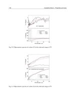
lead to an increase in the red spectral region. The ultraviolet UV and violet V luminescence
are detected in mostly all ion implanted samples at around 290 nm and 410 nm,
respectively, indicating not only extrinsic related ODC or extrinsic defects but also ion
implantation induced defects in the SiO
2
matrix.
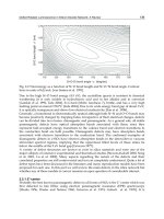
As a surprising peculiarity, the cathodoluminescence spectra of oxygen and sulfur
implanted SiO
2
layers show, besides characteristic bands, a sharp and intensive multimodal
structure beginning in the green region at 500 nm over the yellow-red region and
extending to the near IR measured up to 820 nm. The energy step differences of the
sublevels amount to an average of 120 meV and indicate vibronic-electronic transitions,
probably, of O
¯
2
interstitial molecules, as we could demonstrate by a respective
configuration coordinate model. However, such "mysterious" multimodal luminescence
spectra are observed occasionally in other material compounds too, and are many-fold in
their interpretations by other authors ranging from photonic crystals and interference effects
over discrete quantum dots and respective quantum confinement, even to our model of
interstitial molecules and their electronic-vibronic luminescent transitions.
7. References
Anedda A. , Carbonaro C. M. , Serpi A. , Chiodini N. , Paleari A. , Scotti R. , Spinolo G. ,
Brambilla G. and Pruneri V. : Vacuum ultraviolet absorption spectrum of photorefractive
Sn-doped silica fiber preforms, J. Non-Cryst. Solids 280 (2001) 287.
Anedda A. , Carbonaro C. M. , Clemente F. , Corpino R. , Grandi S. , Mustarelli P. and
Magistris A. : OH-dependence of ultraviolet emission in porous silica, J. Non-Cryst.
Solids 322 (2003b) 68.
Bailey R. C. , Parpia M. , Hupp J. T. : Sensing via optical interference, Materialstoday, Vol 8,
Iss.4, April (2005), 46.
Bakaleinikov L. A. , Zamoryanskaya M. V. , Kolesnikova E. V. , Sokolov V. I. and Flegontova
E. Yu. : Silicon Dioxide Modification by an Electron Beam, Physics of the Solid State 46
(2004) 1018.
Bakos T. , Rashkeev S. N. and Pantelides S. T. : H
2
O and O
2
molecules in amorphous SiO
2
:Defect
formation and annihilation mechanisum , Phys. Rev. B 69 (2004a) 195206.
Bakos T. , Rashkeev S. N. and Pantelides S. T. : Optically active defects in SiO
2
: The
nonbridging oxygen center and interstitial OH molecule, Phys. Rev. B 70 (2004b) 75203.
Barfels T. : PhD dissertation , Kathodolumineszenz amorpher und kristalliner Modifikationen von
SiO
2
und GeO
2
, Rostock university (2001).
Blöchl P. E. : First-principles calculations of defects in oxygen-deficient silica exposed to hydrogen,
Phys. Rev. B 62 (2000) 6158.
Brichard B. , Fernandez A. F. , Ooms H. , Borgermans P. and Berghmans F. : Dependence of
the POR and NBOHC Defects as Function of the Dose in Hydrogen-Treated and Untreated
KU1 Glass Fibers, IEEE Transactions on Nuclear Science 50 (2003) 2024.
Calestani D. , Lazzarini L. , Salviati G. and Zha M. : Morphological, structural and optical study
of quasi-1D SnO
2
nanowires and nanobelts, Cryst. Res. Technol. 40 (2005) 937.
Cannas M. , Agnello S. , Boscaino R. , Costa S. , Gelardi F. M. , Messina F. : Growth of H(II)
centers in natural silica after UV laser exposure, J.Non-Cryst. Solids, 322 (2003b) 90.
Cazaux J. : Some considerations on the electric field induced in insulators by electron bombardment ,
J. Appl. Phys. 59 (1986) 1418.
Silicon Nanocluster in Silicon Dioxide: Cathodoluminescence,
Energy Dispersive X-Ray Analysis and Infrared Spectroscopy Studies
215
Ewig C. S. and Tellinghuisen J. : Ab initio study of the electronic states of O
¯
2
in vacuo and in
simulated ionic solids, J. Chem. Phys. 95 (1991) 1097.
Fitting H J. , Barfels T. , Trukhin A. N. , Schmidt B. , Gulans A. and von Czarnowski A. :
Cathodoluminescence of Ge
+
, Si
+
, and O
+
implanted SiO
2
layers and the role of mobile
oxygen in defect transformation, J. Non-Cryst. Solids 303 (2002b) 218.
Fitting H J. , Ziems T. , von Czarnowski A. and Schmidt B. : Luminescence center
transformation in wet and dry SiO
2
, Radiation Measurements 39 (2004) 649.
Fitting H J. , Ziems T. , Salh R. and von Czarnowski A. : Luminescent defect dynamics in
amorphous SiO
2
:H, phys. stat. sol. (c) 2 (2005a) 693.
Fitting H J. , Ziems T. , Salh R. , Zamoryanskaya M. V. , Kolesnikova K. V., Schmidt B. and
von Czarnowski A. : Cathodoluminescence of wet, dry and Hydrogen-implanted silica
films, J. Non-Cryst. Solids 351 (2005b) 2251.
Fitting H J. , Salh R. , Barfels T. and Schmidt B. : Multimodal Luminescence Spectra of Ion-
implanted Silica, phys. stat. sol. (a) 202 (2005c) R142.
Gerasimova V. I. , Zavorotny Yu. S. , Rybaltovskii A. O. , Chernov P. V. , Sazhin O. D. ,
Khrapko R. R. and Frolov A. A. : Color Centers in Sulfur-Doped Silica Glasses:
Spectroscopic Manifestations of an S
+
2
Interstitial Molecular Ion, Glass Physics and
Chemistry 28 (2002) 5.
Gerasimova V. I. , Rybaltovskii A. O. , Chernov P. V. and Spasskii D. A. : Color Centers in
Sulfur-Doped Silica Glasses: Spectroscopic Manifestations of an SO
2
Interstitial Molecule,
Glass Physics and Chemistry 29 (2003) 232.
Goldberg M. : Cathodoluminescence and cathode-electroluminescence of SiO
2
-layers, PhD thesis,
University of Rostock, (1996).
Gonzalez-Verona O. , Garrido B. , Perez-Rodriguez A. , Morante J. R. , Bonafos C., Carrada
M., Sanz L. F. , Gonzalez M. A. and Jimenez J. : Analysis of the white emission from ion
beam synthesised layers by in-depth resolved scanning photoluminescence microscopy,
Materials Science and Engineering B 91 (2002) 51.
Griscom D. L. : Electron spin resonance investigations of defects and defect processes in amorphous
silicon dioxide, Rev. Solid State Sci. 4 (1990b) 565.
Gu F. , Wang S. F. , Song C. F. , Lu M. K. , Qi Y. X. , Zhou G. J. , Xu D. and Yuan D. R. ;
Synthesis and luminescence properties of SnO
2
nanoparticles, Chem. Phys. Lett. 372
(2003) 451.
Helm C. R. and Deal B. E. (eds.) : The Physics and Chemistry of SiO
2
and the Si-SiO
2
Interface,
Plenum, New York, (1993).
Hosono H. , Weeks R. A. , Imagawa H. and Zuhr R. : Formation of oxygen-deficient type
structural defects and state of ions in SiO
2
glasses implanted with transition metal ions, J.
Non-Cryst. Solids 120 (1990) 250.
Hu J. Q. , Ma J. X. L. , Shang N. G. , Xie Z. Y. , Wong N. B. , Lee C. S. and Lee S. T.: Large-
Scale Rapid Oxidation Synthesis of SnO
2
Nanoribbons, J. Phys. Chem. B 106 (2002) 3823.
Hu J. Q. , Bando Y. and Golberg D. : Self-catalyst growth and optical properties of novel SnO
2
fishbone-like nanoribbons, Chem. Phys. Lett. 372 (2003) 758.
Iacona F., Franzo G. and Spinella C. : Correlation between luminescence and structural properties
of Si nanocrystals, J. Appl. Phys. 87 (2000) 1295
Ivanda M. , Clasen R. , Hornfeck M. and Kiefer W. : Raman spectroscopy on SiO
2
glasses
sintered from nanosized particles, J. Non-Cryst. Solids 322 (2003) 46.
Crystalline Silicon – Properties and Uses
216
Kajihara K. , Skuja L. , Hirano M. and H. Hosono : Diffusion and Reactions of Hydrogen in F
2
-
Laser-Irradiated SiO
2
Glass, Phys. Rev. Lett. 89 (2002) 135507.
Kolesnikova E. V. , Sitnikova A. A. , Sokolov V. I. and Zamoryanskaya M. : Modification of
Silicon Oxide by High Energy Electron Beam, Solid State Phenomena 108-109 (2005)
729.
Kuzuu N. and Horikoshi H. : X-ray induced absorption in fused silica containing various amounts
of OH, J. Appl. Phys. 97 (2005) 93508.
Ledoux G. , Gong J. , Huisken F. , Guillois O. and Reynaud C. : Photoluminescence of size-
separated silicon nanocrystals: Confirmation of quantum confinement, Appl. Phys. Lett.
80 (2002) 4834.
Legrand A. P. : The Surface Properties of Silica, New York, Wiley, (1998).
Lehmann A. , Schumann L. and Hübner K. : Optical Phonos in Amorphous Silicon Oxides,
phys. stat. sol. (b) 121 (1984) 505.
Lopes J. M. J. , Zawislak F. C. , Fichtner P. F. P. , Papaleo R. M. , Lovey F. C. , Condo A. M.
and Tolley A. J. : Formation of epitaxial β-Sn islands at the interface of SiO
2
/Si layers
implanted with Sn ions, Appl. Phys. Lett. 86 (2005a) 191914.
Lopes J. M. J. , Zawislak F. C. , Fichtner P. F. P. , Lovey F. C. and Condo A. M. : Effect of
annealing atmosphere on the structure and luminescence of Sn-implanted SiO
2
layers,
Appl. Phys. Lett. 86 (2005b) 023101.
Lou V. , Sato R. and Tomozawa M. : Hydrogen diffusion in fused silica at high temperatures, J.
Non-Cryst. Solids 315 (2003) 13.
Ma T., Xu J. , Du J. , Li W. , Huang X. and Chen K. : Full color light emission from amorphous
SiCx:H with organic-inorganic structures, J. Appl. Phys. 88 (2000) 6408.
Magruder R. H. , Weeks R. A. and Weller R. A. : Luminescence and absorption in type III silica
implanted with multi-energy Si, O and Ar. ions, J. Non-Cryst. Solids 322 (2003) 58.
Minke M. V. and Jackson K. A. : Diffusion of germanium in silica glass , J. Non-Cryst. Solids
351 (2005) 2310.
Mischler C. , Horbach J. , Kob W. and Binder K. : Water adsorption on amorphous silica surfaces:
a Car-Parrinello simulation study, J. Phys.: Condens. Matter 17 (2005) 4005.
Morimoto Y. , Weeks R. A. , Barnes A. V. , Tolk N. H. and Zuhr R. A. : The effect of ion
implantation on luminescence of a silica, J. Non-Cryst. Solids 196 (1996) 106.
Morimoto Y. and Nozawa S. : Effect of Xe
2
light (7.2 eV) on the infrared and vacuum ultraviolet
absorption properties of hydroxyl groups in silica glass, Phys. Rev. B 59 (1999) 4066.
Mutti P., Ghislotti G. , Bertoni S. , Bonoldi L. , Cerofolini G. F. , Meda L. , Grilli E. and Guzzi
M. : Room-temperature visible luminescence from silicon nanocrystals in silicon implanted
SiO
2
layers, Appl. Phys. Lett. 66 (1995) 851.
Nicklaw C. J. , Pagey M. P. , Pantelides S. T. , Fleetwood D. M. , Schrimpf R. D. , Galloway K.
F. , Wittig J. E. , Howard B. M. , Taw E., McNeil W. H. and Conley J. F. , Jr. : Defects
and Nanocrystals Generated by Si Implantation into a-SiO
2
, IEEE Transactions on
Nuclear Science 47 (2000) 2269.
Ogasawara H. , Brena B. , Nordlund D. , Nyberg M. , Pelmenschikov A. , Pettersson L.G.M.
and Nilsson A. : Structure and Bonding of Water on Pt(111), Phys. Rev. Lett. 89 (2002)
276102.
Pacchioni G. and Mazzeo C. : Paramagnetic centers in Ge-doped silica: A first-principles study,
Phys. Rev. B 62 (2000) 5452.
Silicon Nanocluster in Silicon Dioxide: Cathodoluminescence,
Energy Dispersive X-Ray Analysis and Infrared Spectroscopy Studies
217
Pan B. C. and Biswas R. : Simulation of hydrogen evolution from nano-crystalline silicon, J. Non-
Cryst. Solids 333 (2004) 44.
Perez-Rodriguez A. , Gonzalez-Varona O. , Garrido B. , Pellegrino P. , Morante J. R., Bonafos
C. , Carrada M. and Claverie A. : White luminescence from Si
+
and C
+
ion-implanted
SiO
2
films, J. Appl. Phys. 94 (2003) 254.
Prokes S. M. , Carlos W. E., Veprek S. and Ossadnik C. : Defect studies in as-deposited and
processed nanocrystalline Si/SiO
2
structures, Phys. Rev. B 58 (1998) 15632.
Rashkeev S. N. , Fleetwood D. M. , Schrimpf R. D. and Pantelides S. T. : Defect Generation by
Hydrogen at the Si-SiO
2
Interface, Phys. Rev. Lett. 87 (2001) 165506.
Rebohle L. , von Borany J. , Fröb H. and Skorupa W. : Blue photo- and electroluminescence of
silicon dioxide layers ion-implanted with group IV elements, Appl. Phys. B 71 (2000) 131.
Rebohle L. , Gebel T. , Fröb H. , Reuther H. and Skorupa W. : Ion beam processing for Si/C-rich
thermally grown SiO
2
layers: photoluminescence and microstructure, Appl. Surf. Sci. 184
(2001b) 156.
Rebohle L. , Gebel T. , von Borany J. , Skorupa W. , Helm M. , Pacifici D. , Franzo G. and
Priolo F. : Transient behavior of the strong violet electroluminescence of Ge-implanted SiO
2
layers, Appl. Phys. B 74 (2002a) 53.
Riemann T. , Christen J. , Kaschner A. , Laades A. , Hoffmann A. , Thomsen C., Iwaya M.,
Kamiyama S. , Amano H. and Akasaki I. : Direct observation of Ga-rich microdomains
in crack-free AlGaN grown on patterned GaN/sapphire substrates, Appl. Phys. Lett. 80
(2002) 3093.
Rinnert H. and Vergnat M. : Structure and optical properties of amorphous silicon oxide films with
different porosities, J. Non-Cryst. Solids 320 (2003) 64.
Rodt S. , Seguin R. , Schliwa A. , Pötschke K. and Bimberg D. : International Conference on
Luminescence ICL-05, Beijing, July 25-29, (2005), Book of Abstracts: WED-P-E-01.
Rolfe J. : First excited state of the O
¯
2
, J. Chem. Phys. 70 (1979) 2463.
Salh R. , von Czarnowski A. and Fitting H J. : Multiplet luminescence of sulfur implanted silica-
SiO
2
:S, phys. stat. sol.(a) 202 (2005) R53.
Schweigert I. V. , Lehtinen K. E. J. , Carrier M. J. and Zachariah M. R. : Structure and
properties of silica nanoclusters at high temperatures, Phys. Rev. B 65 (2002) 235410.
Siu G. G. , Wu X. L. , Gu Y. and Bao X. M. : Ultraviolet and blue emission from crystalline SiO
2
coated with LiNbO
3
and LiTaO
3
, Appl. Phys. Lett. 74 (1999) 1812.
Skuja L. N., Silin A. R. and Mares J. : Decay time and properties of luminescence centers in
vitreous silica, phys. stat. sol (a) 50 (1978) 149.
Skuja L. : Isoelectronic series of twofold coordinated Si, Ge, and Sn atoms in glassy SiO
2
: a
luminescence study, J. Non-Cryst. Solids 149 (1992a) 77.
Skuja L. : The origin of the 1.9eV luminescence band in glassy SiO
2
, J. Non-Cryst. Solids 179 (1994a) 51.
Skuja L. : Direct singlet-to-triplet optical absorption and luminescence excitation band of the
twofold-coordinated silicon center in oxygen-deficient glassy SiO
2
, J. Non-Cryst. Solids
167 (1994b) 229.
Skuja L. : Optically active oxygen-deficiency-related centers in amorphous silicon dioxide, J. Non-
Cryst. Solids 239 (1998) 16.
Skuja L. , Hirano M. , Kajihara K. and Hosono H. : Point defect creation by photochemical
processes in glassy silica, Phys. Chem. Glasses 43C (2002) 145.
Stevens-Kalceff M. A. : Cathodoluminescence microcharacterization of the defect structure of
irradiated hydratedand anhydrous fused silicon dioxide, Phys. Rev. B 57 (1998) 5674.
Crystalline Silicon – Properties and Uses
218
Tandon P. : Chemical annealing of oxygen hole centers in bulk glasses, J. Non-Cryst. Solids 336
(2004) 212.
Torchynska T.V. : Photoluminescence of Si nanocrystallites in different types of matrices, J. Non-
Cryst. Solids 352 (2006) 2484.
Trukhin A. N. : Self-trapped exciton luminescence in α-quartz, Nucl. Instr. and Meth. in Phys.
Res. B 91 (1994) 334.
Trukhin A. N. , Goldberg M. , Jansons J. , Fitting H J. and Tale I. A. : Silicon dioxide thin film
luminescence in comparison with bulk silica, J. Non-Cryst. Solids 223 (1998) 114.
Trukhin A. N. and Fitting H J. : Investigation of optical and radiation properties of oxygen
deficient silica glasses, J. Non-Cryst. Solids 248 (1999) 49.
Trukhin A. N. , Fitting H J. , Barfels T. and von Czarnowski A. : Cathodoluminescence and IR
absorption of oxygen deficient silica-Influence of hydrogen treatment, J. Non-Cryst. Solids
260 (1999) 132.
Trukhin A. N. , Jansons J. , Fitting H J. , Barfels T. and Schmidt B. : Cathodoluminescence decay
kinetics in Ge
+
, Si
+
, O
+
implanted SiO
2
layers, J. Non-Cryst. Solids 331 (2003a) 91.
Tsu D. V. , Lucovsky G. and Davidson B. N. : Effects of the nearest neighbors and the alloy matrix
on SiH stretching vibrations in the amorphous SiO
r
:H (0<r<2) alloy system, Phys. Rev. B
40 (1989) 1795.
Wilkinson A. R. and Elliman R. G. : The effect of annealing environment on the luminescence of
silicon nanocrystals in silica, J. Appl. Phys. 96 (2004) 4018.
Wu X. , Zou B. , Xu J. , Yu B. , Tang G. , Zhang G. and Chen W., Nanostruct. Mat. 8 (1997) 179.
Xu Q. , Sharp I.D. , Liao C.Y. , Yi D. O. , Ager III J. W. , Beeman J. W. , Yu K. M. , Chrzan D.
C. and Haller E. E. : Germanium Nanocrystals Embedded in Sapphire, Lawrence
Berkeley National Laboratory, University of California, Paper LBNL-57463, (2005).
Yao B. , Shi H. , Zhang X. and Zhang L. : Ultraviolet photoluminescence from nonbridging oxygen
hole centers in porous silica, Appl. Phys. Lett. 78 (2001) 174.
Yi L. X. , Heitmann J. , Scholz R. and Zacharias M. : Phase separation of thin SiO layers in amorphous
SiO/SiO
2
superlattice during annealing, J. Phys. : Condens. Matter 15 (2003) S2887.
Yu Y. H. , Wong S. P. and Wilson I. H. : Visible Photoluminescencein Carbon-Implanted Thermal
SiO
2
Films, phys. stat. sol. (a) 168 (1998) 531.
Zacharias M. , Heitmann J. , Scholz R. , Kahler U. , Schmidt M. and Bläsing J. : Size-controlled
highly luminescent silicon nanocrystals: A SiO/SiO
2
superlattice approach, Appl. Phys.
Lett. 80 (2002) 661.
Zacharias M. , Yi L. X. , Heitmann J. , Scholz R. , Reiche M. and Gösele U. : Size-controlled Si
nanocrystals for photonic and electronic applications, Solis State Phenomena 94 (2003) 95.
Zavorotny Yu. S. , Lutsko E. V. , Rybaltovskii A. O. , Chernov P. V. , Sokolov V. O. and
Khrapko R. R. : Color Centers in Sulfur-Doped Silica Glass: Spectroscopic Manifestations
of an Interstitial Molecule S
2
, Glass Physics and Chemistry 27 (2001) 331.
Zhang Q. , Bayliss S. C. and Frentrup W. : The stable blue and unstable UV photoluminescence from
carbon nanoclusters embedded in SiO
2
matrices, Solid State Commun. 99 (1996) 883.
Zhao J. , Mao D. S. , Lin Z. X. , Jiang B. Y. , Yu Y. H. , Liu X. H. , Wang H. Z. and Yang G. Q. :
Intense short-wavelength photoluminescence from thermal SiO
2
films co-implanted with Si
and C ions, Appl. Phys. Lett. 73 (1998) 1838.
Zorenko Y. , Gorbenko V. , Voloshinovskii A. , Stryganyuk G. , Nedilko S. , Degoda V. and
Chukova O. : Luminescence of Sc-related centers in single crystalline films of Lu
3
Al
5
O
12
garnet, phys. stat. sol. (c) 2 (2005) 105.
10
Nanocrystalline Porous Silicon
Sukumar Basu and Jayita Kanungo
IC Design & Fabrication Centre
Dept. of Electronics and Telecommunication Engineering, Jadavpur University
India
1. Introduction
Porous silicon can be considered as a silicon crystal having a network of voids in it. The
nano sized voids in the bulk silicon result in a sponge-like structure of pores and channels
surrounded by a skeleton of crystalline Si nano wires. Porous silicon (PS) is gaining
scientific and technological attention as a potential platform mainly for its multifarious
applications in sensing and photonic devices (Canham, 1997a; Pavesi & Dubos;1997;
Dimitrov,1995; Tsamis et al., 2002; Archer & Fauchet, 2003; Barillaro et al.,2003). The
extremely large surface to volume ratio (500m
2
/cm
3
) of PS, the ease of its formation,
control of the surface morphology through variation of the formation parameters and its
compatibility to silicon IC technology leading to an amenability to the development of smart
systems-on-chip sensors have made it a very attractive material. Due to these multi
functional applications of PS, recently it has been proposed to be an educational vehicle for
introducing nanotechnology and inter-disciplinary material science by eminent scientists
working in this field. But in order to develop porous silicon based devices and their
integration to electronic circuits the low resistance stable electrical contacts are necessary.
However, unlike crystalline silicon the outstanding problem with PS is the instability of its
native interface with a metastable Si–H
x
termination (Tsai et al.,1991). The metastable hydro-
silicon can undergo spontaneous oxidation in ambient atmosphere and results in the
degradation of surface structures. This also creates problems to get a stable Ohmic contact
(Deresmes et al.,1995; Stievenard & Deresmes, 1995) which is again a very important factor
regarding its commercial applications. Therefore passivation of surface is necessary to make
stable porous silicon based devices. For that purpose substituting surface hydrogen by
another chemical species has appeared desirable. Oxidations (Rossi et al, 2001; Bsiesy, et al
1991; Petrova-Koch et al., 1992) nitradation (Anderson et al., 1993) and halogenetion
(Lauerhaas & Sailor, 1993) are found to be useful for PS surface passivation. Derivatisation
by organic groups and polymer (Lees et al. 2003; Mandal et al. 2006), offers an alternative
possibility to stabilize the material. Metals like Cu, Ag, In etc. were also used to modify the
porous silicon surface to stabilize its photoluminescence properties (Andsager et al 1994;
Steiner et al., 1994). Surface modification of PS using noble metals like Pd and Pt has also
been studied recently (Kanungo et al. 2009a).
The details on PS are given in a comprehensive review published by Cullis et al. (Cullis et
al., 1997) and in the handbook on Porous Silicon properties edited by Canham (Canham,
1997a). H. Foll et al. (Foll et al. 2002) and V. Parkhutik (Parkhutik, 1999) also elaborately
reviewed the formation and applications of porous silicon.
Crystalline Silicon – Properties and Uses
220
2. Preparation of nanocrystalline porous silicon using different chemical
methods
Several methods are developed to make the porous layer with wide variation of pore
morphologies having the pore dimensions from micro to nanometers. Chemical etching of
silicon using chemical solutions of HF, HNO
3
and water (Vasquez et al., 1992), NaNO
2
and
HF or CrO
3
and HF(Beale et al., 1986; Zubko et al. 1999) are employed for PS formation.
However, the most widely used method is the electrochemical etching of silicon crystal in an
electrolyte solution of HF and ethanol or methanol (Saha et al., 1998; Kanungo et al., 2006) or
HF and water or HF and N, N dimethyl formamide (DMF) (Archer et al., 2005) by passing
current for a fixed duration of time. Hummel et al. (Hummel & Chang, 1992) utilized a new
spark erosion technique for PS formation, which does not involve any aqueous solution or
fluorine contaminants in air or in the other gases. Another interested development in this
area is the magnetic field assisted anodization technique employed by T. Nakagawa et al.
(Nakagawa et al., 1996). Recently Y. Y. Xu, et al. (Xu, et al. 2005) describe hydrothermal
etching of crystalline silicon in HF containing ferric nitrate to obtain the large quantities of
regular, uniformly distributed silicon nano pillars which are perpendicular to the surface
and well separated from each other. In addition, perpendicular electric field assisted
method, illumination assisted method, Hall effect assisted method, lateral electric field
method, Buried P-layer assisted method and their combinations have been very recently
reported (Samuel, BJ., 2010).
In most cases, the porous silicon structure is formed by electrochemical etching of Si wafers
in electrolytes including hydrofluoric acid (HF) and ethanol. The cleaned, polished Si wafer
surface is hydrophobic. Added absolute alcohol increases the wettability of the substrate
and thus helps the electrolyte penetrating into the pores. So laterally homogenous current
density can be maintained to result in the formation of uniform PS layers. The added
ethanol also helps in removing the H
2
bubble from the sample surface formed during the
anodization process. To get the uniform porous layers with high reproducibility, the applied
anodic current density, etching time and the electrolyte concentration are controlled
precisely during the process. The cathode of the anodization cell is generally made of
platinum or other HF-resistant conductive material. Platinum is used as cathode and Si
surface itself acts as the anode. In Fig. 1, a conventional single tank setup is shown both for
vertical and horizontal field application.
To get the nanocrystalline porous silicon on n-type silicon, illumination method (Samuel,
BJ., 2010). is the most popular way to generate holes required in the electrochemical etching
process (Fig.2). However, the photo energy absorption by the atoms depends on the
intensity of the illumination source, the distance from the source and the electrolyte
environment. Therefore, only the surface layer under the illumination generates electron
hole pairs. But the etching rate gradually decreases with time as it is very difficult to reach
the illumination into the deep area of the pores.
An alternative Hall Effect assisted method (Fig.3a) can be used for n-type porous silicon
formation (Samuel, BJ., 2010). In this arrangement the sample is exposed to the Hall Effect
environment. By applying a very large bias voltage and a large magnetic field, the upper
layer of the semiconductor is depleted of electrons and is then inverted from n-type to p-
type (Fig. 3b). The accumulated hole on the upper layer can participate in the chemical
reactions during the etching process. Two main advantages of this method are (i) the
Nanocrystalline Porous Silicon
221
illumination sources are not required and (ii) no metal electrodes are needed for etching.
Therefore, an etching container devoid of illumination and free of metal electrode can be
well designed for the safety of handling the corrosive HF electrolyte so that the
contamination from the metal electrode could be avoided.
Fig. 1. Schematic of cross sectional view of the jig used for PS formation by electrochemical
anodization by the application of electric field in (a) vertical and (b) horizontal mode.
Fig. 2. Schematic of the experimental setup of the illumination assisted method.
A buried p-layer assisted method (Samuel, BJ., 2010) is also proposed for n-type porous
silicon fabrication. The buried p-layer acts as the source of hole and is placed underneath the
n-layer (Fig.4). The proposed buried p-layer assisted method can also be superimposed on
the illumination assisted method during the electrochemical anodization.
Crystalline Silicon – Properties and Uses
222
Fig. 3. Schematic of the (a) experimental setup of Hall effect assisted method and (b) the
mechanism of pore formation [with the permission of Nova Science Publishers, USA].
Fig. 4. The schematic mechanism of the biased pn structures for buried p-layer assisted
method [with the permission of Nova Science Publishers, USA].
2.1 Mechanism of silicon dissolution and pore formation
Although the complete understanding of the Si dissolution mechanism is still under study,
the mostly accepted theory describes that holes are required for pore formation. During the
anodization process, the positively charged Si surface is oxidized by F
-
ions followed by the
formation of water-soluble H
2
SiF
6
complex as shown in Fig.5. For the pore formation, the
anodic reactions can be depicted as
Si + 6HF → H
2
SiF
6
+ H
2
+ 2H
+
+ 2e
-
. (1)
However, the detail chemical steps during PS formation may be expressed as follows;
Si + 2HF + 2h
+
SiF
2
+ 2H
+
SiF
2
+ 4HF H
2
+ H
2
SiF
6
(for divalent anodic reaction)
Si + 4HF + 4h
+
SiF
4
+ 4H
+
Nanocrystalline Porous Silicon
223
SiF
4
+ 2HF H
2
SiF
6
(for tetravalent anodic reaction)
Different models are also proposed to explain the formation of porous silicon and the pore
morphology. According to the model suggested by Kang and Jorne (Kang & Jorne, 1993) the
distance between the pores varies as a square root of the applied voltage. The model by
Beale et al (Beale et al. 1985) shown in Fig. 5a highlights a quantitative idea about the pore
morphology. They pointed out that there is a space charge region between the PS layer and
bulk silicon. This model further considers the pinning of the Fermi level at the Si/electrolyte
interface. It is due to a large number of surface states that create Schottky barrier between
the semiconductor and the electrolyte. The decrease of the Schottky barrier height occurs
due to the dissolution of the pore tips because of the electric field generated in that region.
Fig. 5. The schematic of the (a) Beale model and (b) The diffusion – limited model (Samuel,
BJ., 2010) [with the permission of Nova Science Publishers, USA].
The distribution of the electric field in the pore tips can be estimated by the model proposed
by Zhang (Zhang, 1991) that also gives reasonable explanation of the localized dissolution of
silicon. According to this model PS growth takes place through anodic oxidation and
dissolution through direct etching of silicon in HF.
The diffusion-limited model in Fig. 5b proposed by Smith and Collins was the first
computer simulated theoretical model. According to this theory the holes diffuse to the Si
surface and react with the surface atoms (Samuel, BJ., 2010)
Recently Lehamann proposed a model (Fig. 6) that considers the quantum confinement of
charge carriers on the pore walls due to their small thickness and it may be responsible for
the pore formation (Samuel, BJ., 2010).
The explanation of pore nucleation, pore structure and the importance of the formation
parameters etc. during PS formation has been provided in the model proposed by
Parkhutik and Shershulsky (Parkhutik & Shershulsky, 1992). According to this model the
bottoms of the pores are covered by a virtual passive layer (VPL) that prevents a direct
contact between the electrolyte and the substrate. When the electric field is applied the
dissolution of VPL takes place and the pores are formed. The growth of VPL and its
dissolution are exponentially related to the electric field strength and are dependent on
the chemical reactivity of the material towards the electrolyte and other experimental
parameters.
Crystalline Silicon – Properties and Uses
224
Fig. 6. The schematic of the proposed quantum model of Lehamann (Samuel, BJ., 2010)
[with the permission of Nova Science Publishers, USA].
A new model on the mechanism of the pore growth suggests that the pore propagation into
the crystal volume is a process that is controlled not only by the electrochemical factors, but
also by mechanical stresses and hydrogen-related defects in Si. The PS growth is the
alignment of the pore nucleation sites along the crystal defects of the Si surface. The defects
serve as easy paths for the pore propagation. The dynamic stress during pore growth is
another important issue. At the bottom of each pore, the dissolution reaction liberates the
essential amount of hydrogen (Parkhutik, 1999). Outward movement of gas bubbles and
products of Si dissolution together with inward propagation of fresh electrolyte are to
produce essential hydrodynamic pressure inside the porous silicon layer. According to the
theory of propulsion the essential tensile stresses are produced both in porous silicon and in
Si substrates. Therefore, the micro cracks are formed in PS (Fig. 7) and that serve as easy
path for further pore growth.
Fig. 7. Schematic of the pore growth according to the mechanical stress assisted mechanism
of porous silicon (V. Parkhutik, 1999)
Nanocrystalline Porous Silicon
225
3. Properties of nanocrystalline porous silicon
The pore morphology of the PS layer characterized by the void fraction or porosity, the
mean size of the pores, the pore size distribution, the interconnectivity of the pores, the
passivation and mean size of the skeleton enclosing the pores depends on the formation
parameters of PS, the additives in the electrolyte solution and the doping concentration of
the silicon wafer. However, vertically grown uniform pores can also be developed in n-type
c-Si using photolithography.
3.1 Structural properties of porous silicon
The main structural parameters of the porous silicon are the pore type, pore size, porosity
and porous thickness. FESEM, TEM, AFM etc are commonly used to study the porous
silicon structure. Fig. 8 shows the FESEM of nano and macro porous silicon as developed in
the authors’ laboratory.
Fig. 8. FESEM of (a) nano porous and (b) macro porous silicon surfaces.
Most of the pores in porous silicon are closed at one end and they are inter connected to
each other. Pores open at both ends i.e. the free standing porous silicon can also be realized
in membrane structure. The cylindrical pore with ‘branching’ is very common in porous
silicon. But for nano porous silicon a gradual decrease in pore size with depth in thick
porous layer is observed. This arises due to the secondary dissolution since the top layer is
exposed to the electrolyte longer than the bottom layer. Pore size is also a very important
parameter for the PS based sensing devices. The nano, meso and macro porous silicon are
defined in Table 1 according to the IUPAC guideline (Canham, 1997a),
Pore width Pore type
< 2 nm Micro porous/ nano porous
2 nm - 50 nm Meso porous
> 50 nm Macro porous
Table 1. IUPAC classification of pore size
Crystalline Silicon – Properties and Uses
226
The porosity of a sample is defined as the fraction of void in the porous structure. The
porosity (P) and thickness (t) are determined by the relations:
P= (m
1
-m
2
) / (m
1
-m
3
)
t = (m
1
-m
3
) / (ρ×A)
Where m
1,
the mass of the sample before porous silicon formation, m
2
, the mass after
formation and m
3
, the mass of the sample after complete dissolution of the porous layer by
20% NaOH solution. ρ is the density of bulk silicon and A is the area of the porous silicon
layer. The masses m
2
and m
3
are measured after drying the samples properly in the vacuum
environment.
The porosity, thickness, pore diameter and microstructure of porous silicon depend on the
formation parameters like composition of electrolyte, anodization current density, etching
time, temperature, ambient humidity, wafer type and resistivity, illumination, and drying
conditions (Table 2).
Increasing the values of Porosity Etching rate
HF concentration Decreases Decreases
Current density Increases Increases
Anodization time Slightly increases Slightly decreases
Wafer doping (p-type) Decreases Increases
Wafer doping (n-type) Increases Increases
Table 2. Effect of anodization conditions on the formation of porous silicon (Bisi et al. 2000).
3.2 Chemical properties of porous silicon
Porous silicon has a very high surface area. Therefore, it contains a high density of Si
dangling bonds and impurities such as hydrogen and fluorine that are residuals from the
electrolyte used during PS formation. After the formation, initially porous layer is covered
by SiHx (x = 1, 2, 3) bond that remains on the surface even after rinsing and drying the
samples. However, it disappears during annealing at 300-500°C (Vázsonyi et al. 1993).
The PS surface oxidizes spontaneously if it is kept in the ambient air for a few hours and the
process continues until the whole surface is oxidized. Illumination and increased
temperature enhance the oxidation reaction rate. A blue shift in the luminescence spectra
occurs after oxidation of the surface (Hossain et al. 2000, Karacali et al. 2003). It also affects
the electrical conductivity and the optical properties of the porous layer (Astrova et al. 1999).
The common impurity in freshly prepared porous silicon is fluorine. The concentration of
fluorine depends on the type of electrolyte used. It is commonly found in the form of SiFx (x
= 1, 2, 3). The fluoride concentration decreases with time (Petit et al. 1997), probably due to
the replacement of SiF bonds by SiOH bonds through reactions with water vapor content of
the ambient air.
3.3 Physical properties of porous silicon
3.3.1 Young’s modulus
It is reported (Barla et al. in 1984) that PS should behave similar to the starting Si single
crystal but the lattice mismatch occurs at the Si-PS interface due to its nanostructure and
that may be the reason of different Young’s modulus value of PS. The Young’s modulus of
Nanocrystalline Porous Silicon
227
porous silicon has been investigated by using X-ray diffraction, acoustic wave propagation
and nanoindentation technique. The data measured from these different techniques are in
good agreement and it is observed that for the PS layer the Young’s modulus decreases with
increasing porosity as shown in Table 3 (Bellet 1997). Also the micro hardness of the PS layer
decreases with the increasing porosity (Duttagupta et al. 1997).
Sample Method of investigation Porosity (%) Youn’s modulus (GPa)
p
+
Acoustic technique 20 82.9
p
+
Acoustic technique 28 60
p
+
Acoustic technique 32 50.3
p
+
X-ray 34 41
p
+
X-ray 54 17
p
+
X-ray 74 11
p
+
Nanoindentation 80 5.5
p
+
Nanoindentation 90 0.87
Table 3. Young’s modulus values of porous silicon deduced from different techniques.
(Bellet, 1997)
3.3.2 Thermal conductivity
Nano porous silicon is a good thermal insulator. As reported in the literature the thermal
conductivity of PS decreases with the porosity and in the case of nanoporous structures the
thermal conductivity depends on the formation parameters. (Lang 1997).
Table 4 presents the experimental data for the thermal conductivity obtained from the
literature. Electrically induced thermal wave were analyzed for thermal conductivity
measurements by Lang et al. Photo thermal reflectance analysis and photoacoustic
spectroscopy were also used by the other groups for the thermal conductivity
measurements. However, the values given in the literature shows dramatic differences for
different techniques.
Sample Morphology Porosity (%)
Thermal
conductivity
(as prepared)
Wm
-1
K
-1
Thermal
conductivity (after
300
0
C prepared)
Wm
-1
K
-1
p-type Nano porous 40 1.2 1.3
p-type Meso porous 45 80 2.7
n-type Nano+ macro 53 1.75 1.85
Table 4. Experimental data of thermal conductivity of porous silicon (W Lang, 1997)
As reported in the literature, due to the small size of structures, the thermal conductivity of
p-type nanoporous silicon is 1.2 Wm
-1
K
-1
, which is less than the thermal conductivity of the
silicon oxide. This is because of the nanostructure that does not transport heat easily and
also the pores prevent the heat transfer from one elemental crystallite to the next. But when
the material is partially oxidized, the thermal conductivity increases slightly. It is because of
the incorporation of the oxygen into the structure, due to which the porosity decreases and
as a result heat transport increases.
Crystalline Silicon – Properties and Uses
228
But for meso porous silicon crystallites are connected by small bridges that are oxidized at
low temperature and create heat barrier, which must be overcome during the heat transport
process. As a result the thermal conductivity decreases.
3.3.3 Electrical resistivity
The electrical resistivity of the PS layer is very high due to its nano structure. Four probe
method is very commonly used for the conventional determination of the resistivity of
porous silicon. But PS is very sensitive to the ambient atmosphere. So it is difficult to
determine the exact values for the PS resistivity (Ben-Chorin, 1997). The resistivity of porous
silicon changes with the porosity of the sample as it depends on the quantum confinement,
mobility and drift of the carriers, changes in the band structure, temperature and on the
medium inside the pores (Parkhutik, 1999).
To a large extent the low porosity material behaves like intrinsic bulk Si. The barrier heights
are similar to the bulk silicon which suggests that the Fermi level lies near the mid-gap
position. But the drift mobility of the majority carriers is order of magnitude lower than the
bulk silicon. (Ben-Chorin 1997). Thermally activated carriers move in extended states, but
multiple trapping in the surface states disturbs their motion. Therefore, the drift mobility is
very low. And as the traps are energetically distributed throughout the gap, hopping
between these states at high frequencies gives rise to a temperature independent AC
conductivity
A strong increase of resistivity (10
10
-10
12
Ωcm) of highly porous silicon was observed for
high porosity samples due to the quantum confinement effect that results in a modulation of
the effective bandgap. For these samples the AC conductivity is almost temperature
independent at high frequencies (Ben-Chorin 1997). A non linear dependence of the
conductivity with the applied voltage was observed for these samples. It is suggested that
two parallel processes are involved in current conduction (Ben-Chorin 1997). The first one is
the hopping transport of the carrier and the second one is the conduction due to the thermo-
ionic emission .
Both the low and high porosity samples are very sensitive to the environment. The exposure
of the porous layer to the vapour of the polar solvents affects the conductivity. The
conductivity depends exponentially on the partial pressure of the solvent and on its dipole
moment.
3.3.4 Optical and optoelectronic properties
3.3.4.1 Refractive index
The effective refractive index of PS depends on the porosity, the impurities on the surface of
porous silicon and the refractive index of the materials filling the pores. The refractive index
of an oxidized PS layer is lower than the non-oxidized layer having the same porosity.
3.3.4.2 Absorption co-efficients
The absorption coefficient of the PS layer indicates the correlation between the bandgap and
the porosity that is mainly due to the quantum confinement effect. (Bisi et al. 2000, Behren &
Fauchet 1997). The absorption coefficient of porous silicon can be measured by optical
transmission, photoluminescence excitation and photo thermal deflection spectroscopy. For
a free standing PS layer the optical transmission method is very sensitive. In this case Fabry-
Perot interference fringes are used to determine the refractive index. The absorption
Nanocrystalline Porous Silicon
229
coefficient is then calculated including both the multiple interference effect and the sample
reflection. The absolute value of absorption coefficient can be obtained by the
photoluminescence excitation method but not by photo thermal deflection spectroscopy
(PDS). In fact, PDS is effective for estimating very low values of the absorption coefficient
below the crystalline Si band gap.
As expected for an indirect band gap material, a linear behaviour of the transmission spectra
of crystalline Si and p
+
PS were observed. But a non linear dependence of the absorption
coefficient on photon energy was obtained for p-type porous silicon with an absorption blue
shift with respect to crystalline Silicon as reported (Bisi et al. 2000). It is determined from the
Raman experiment that the blue shift is correlated with the smaller average crystallite
diameter and the quantum confinement is considered as the key factor for the absorption in
porous silicon.
3.3.4.3 Photoluminescence
Porous silicon shows photoluminescence at wavelengths ranging from the ultraviolet (Lin
et al., 1996) to the infrared due to radiative recombination of the carriers confined in
nanoclusters of Si embedded into the walls of PS layer. However, the physical mechanisms
of photoluminescence from porous silicon are still the subjects of controversy. The most
available reports on PL bands of porous silicon are available in different spectral regions e.g.
(i) ultraviolet band, (ii) Visible band and iii) Infrared PL band. The following are the
characteristics of different PL bands of porous silicon.
i. Ultraviolet PL band (<500 nm):
a. UV PL band in room temperature occurs mainly due to the oxidized porous silicon
b. PL shows a red shift in the peak intensity with time.
c. PL get quenched when exposed to methanol.
d. PL intensity and peak intensity are stable under illumination.
ii. Visible PL band (500nm-800nm):
a. It requires silicon crystallites to get visible PL from porous silicon
b. Peak wavelength decreases as crystal size decreases.
c. PL intensity increases and a blue shift occurs with time.
d. Blue shift in peak wavelength occurs with surface passivation by hydrogen or by
oxidation.
iii. Infrared PL band (800nm-2 μm):
a. The radiative electron capture at positively charged dangling bonds on the surface of
the silicon branches is responsible for the infrared PL band.
b. Sometimes this band is referred as the tunable IR band as the peak energy of this IR
band is shifted as a function of porosity.
c. The relative intensity of the IR PL band increases with time.
d. The PL intensity is totally quenched at higher temperatures of around 450°C.
The following models of the photoluminescence from PS have been proposed following the
classification by Canham (Cullis & Canham, 1991),
a. Quantum confinement:
Quantum confinement within the nanometer size silicon branches of the porous silicon is
responsible for direct band-to-band recombination and thus the origin of PL (Streetman,
1990). With decreasing crystal size a blue shift is observed (Canham, 1990a) because the
reducing crystal size causes a further widening of the band gap. The band-gap energy shift
Crystalline Silicon – Properties and Uses
230
of silicon with temperature followed by the thermal broadening can explain the observed
temperature dependence of the PL (Lockwood et al. 1992).
b. Nano-crystal surface states:
Due to quantum confinement effect (Koch, 1993) absorption of the carriers occurs in the
silicon crystallites and as a result the recombination centers are formed due to an adjustment
of the bond lengths and bond angles by silicon atoms at the surface of the crystallite. This
adjustment leads to the formation of a number of traps or so called surface states within the
band gap. Probably due to the confinement of the carriers in these states radiative
recombine occurs by a tunneling mechanism and gives rise to PL.
c. Specific defects and spurious molecules:
The surface hydrides on the branches of the porous silicon (Tsai, 1991) are possibly responsible
for the ‘red’ band PL. The tunable visible PL in PS may be attributed to SiHx groups (Wolford
et al., 1983). This may be further confirmed from the fact that on heat treatment (Prokes et al ,
1992) hydrogen is desorbed from the porous silicon and thus the quenching of the PL with
temperature (Cullis et al, 1997) due to presence of non-radiative dangling bonds. Further there
is a report that surface molecules, specifically siloxene, a by-product of the anodization process
and remaining on the surface of the porous silicon (Hamilton , 1995), may be responsible for
‘red’ PL band (Fuchs et al., 1992). After annealing at 400°C siloxene has an attractive
luminescent property similar to porous silicon (Stathis & Kastner , 1987) .
d. Structurally disordered phases:
A significant amount of amorphous silicon was reported to contain within porous silicon
(Perez et al., 1992). It is known that hydrogenated amorphous silicon (a-Si:H) can produce
visible PL (Vasquez, 1985) and so it was suggested that a-Si:H might be responsible for ‘red’
PL band (Vasquez et al. 1992) The observed tunability of the PL was further suggested as
due to introduction of hydrogen into the amorphous silicon in varying amounts (Cullis &
Canham,1991).
3.3.4.4 Electro luminescence
The third form of the luminescence is the electro luminescence, which is tunable by an
electric field applied on the sample (Halimaoui et al. 1991). PS produces different
luminescent properties. ‘The origin of luminescent phenomena is the quantum confinement
in the nanostructure Si wires of porous silicon.’ With increasing porosity crystallites
dimension decreases and the band gap increases thereby shifting the peaks in the
luminescence spectra (Read et al. 1992). As reported in the literature, the EL spectra show a
blue shift with an increasing bias. However, the mechanisms of the electro luminescence in
PS are not studied in detail. In fact, the absence of reliable electrical contact to PS due to the
rough surface of silicon was so far the major difficulty in doing this study.
3.3.4.5 Cathodoluminescence
During the structural SEM or TEM study on PS Cathodoluminescence could be observed.
The peak of Cathodoluminescence (CL) is extremely weak and unstable. But when SiO
2
is
present stable and brighter CL could be achieved (Williams 1997). Piillai et al. (Piillai et al.,
1992) suggested that during the SEM or TEM study the KeV electron beam may excite
several high energy defect states of an unspecified molecules attached to the PS surface and
their optical de-excitation gives the CL emission.
4. Surface stabilization of NPS by different methods
In spite of all other advantages, the major barrier preventing commercial applications of PS
is the instability of its native interface with metastable Si–H
x
termination. The metastable
Nanocrystalline Porous Silicon
231
hydro-silicon undergoes spontaneous oxidation in ambient atmosphere and results in the
degradation of surface structures. This creates problem for taking good electrical contacts on
PS, important for its commercial applications (Fig. 9). Therefore, the passivation of PS
surface is necessary to make it possible to fabricate the stable devices based on porous
silicon.
Fig. 9. Band diagram of Al/PS junction (for Ohmic contact to p type semiconductor Φm>Φs)
(a) before surface modification (Fermi level is pinned by the PS surface states) and (b) after
surface modification (Fermi level become unpinned and it can move under the applied bias).
In 1965, Beckmann (Beckmann , 1965) observed that during a long storage in ambient air the
PS film gets oxidized. This chemical conversion is slow and basically similar to the ageing of
Si wafers i.e. a native oxide layer forms on the surface of pores. Due to the ageing effect, the
structural (Astrova et al. 2002), electrical and optical properties (Karacali et al., 2003) of PS
showed continuous change with the time. The growth of the native oxide was completed
approximately after one year (Petrova, et al., 2000). In order to avoid the transient period of
ageing, substitution of surface hydrogen by another chemical species appeared desirable.
Chemical, anodic, dry and wet thermal oxidation processes were investigated and presented
by Rossi et al.in 2001. Anodic oxidation showed some improvement against ageing in air but
rapid thermal oxidation appeared to give more optimum results, in providing PS samples
with good electronic surface passivation and improved stability against ageing for optical
measurements. For stabilization of the porous silicon surface, derivatisation by organic
groups and polymer offers an alternative possibility to oxidation. Nitradation and
halogenetion were also studied to stabilize the PS surface. Metals like Cu, Ag, In etc. were
also used to modify the porous silicon surface to stabilize its photoluminescence properties.
The metal electrode contact to the unmodified PS surface for the electrical measurements
may exhibit an unstable and rectifying behaviour, because PS surface states that arise due to
its nano structure can act as the recombination centers. Therefore, the passivation of defect
states in porous silicon is necessary to get a stable and reliable electrical contact to PS. There
is an existing challenge for the fabrication of reproducible low resistance Ohmic contacts on
porous silicon and it is indispensable for porous silicon based electronic devices. The PS
layer contains huge number of volume traps and interface states, resulting in the Fermi-level
pinning at the PS–Si interface. This may block the electrical response of the PS–Si structure.
In a recent work the problem of contact on porous silicon was bypassed by taking contacts
Crystalline Silicon – Properties and Uses
232
from the back of the silicon substrate for capacitive sensors. A few reports are available on
the formation of electrical contact to porous silicon. Zimin et al. (Zimin et al., 1995) reported
a lateral Al ohmic contact to n type PS having a contact resistivity of the order of 10
-3
to 10
-2
Ω cm
2
for low porosity and low resistivity samples but they observed a rectifying behaviour
for high resistive PS, both n and p type. Martin Palma and co-workers (Martin-Palma et al.,
1999) reported the same for the Al-PS-Si-Al sandwich structure, which showed rectifying
behavior even after prolonged exposure to the atmosphere. There are also reports on
metallic contacts to PS using Au, In, Au-In, In-Sn, Al etc and all the contacts showed
Schottky behavior (Angelescu & Kleps, 1998). Electroless Ni deposition was studied for
getting metal contact to PS and an Ohmic behaviour was observed only for low bias
voltages. H. A. Andersson et al. (Andersson et al., 2008) performed an experiment to
examine the morphology and the properties of Ni obtained by electro less deposition on
p-type PS and subsequent formation of Ni silicide by heat treatment. They showed that both
rectifying and Ohmic contacts could be formed between electro less deposited Ni and
PS depending upon the heat treatment conditions. Reports (Jeske et al., 1995) are also
available on the use of electro less deposited Au, Cu and Ni contact to porous silicon.
Although Au and Cu showed some positive results Ni was proved to be ineffective for
Ohmic contact.
The stabilization of PS surface by noble metals for reliable metal contact has been recently
reported by us (Kanungo et al. 2009a). We used the noble metal (Pd, Pt, and Ru) ions to
stabilize the surface of porous silicon. Porous silicon surfaces were modified at room
temperature by electroless method using acidic aqueous solutions of PdCl
2,
RuCl
3
and
K
2
PtCl
6
to passivate the PS surface by the
noble metals like Palladium (Pd), Ruthenium (Ru)
and Platinum (Pt) respectively. To remove the native oxide layer from the PS surface, prior
to modification the samples were dipped into 10% HF solution for 10 sec and were then
immediately dipped into the different chloride solutions. Subsequently the samples were
rinsed gently by DI water and dried followed by annealing in air at 110
0
C inside an electric
oven for 10 min to evaporate the residual solvent present in the samples. The flow chart of
the surface modification steps is given in Fig. 10.
To optimize the solution strength and modification time a number of experiments was
carried out with different concentrations (0.1 M, 0.05 M, 0.01 M, 0.005 M, 0.001 M) of the
solution and different modification time (5 sec – 180 sec). The stability and reproducibility
were checked by taking I-V measurements.
The chemical modification steps are cited as follows:
[M]Cl
Z
[M]
Z+
+ ZCl
-
Where, [M] = Pd, Ru and Pt.
[M]
Z+
[M] (Island) + Zh
+
Si + 2H
2
O + 2h
+
Si(OH)
2
+ 2H
+
Si(OH)
2
SiO
2
+ 2H
+
+ 2e
-
2H
+
+2e
-
H
2
2Cl
-
+ 2H
+
2HCl
Nanocrystalline Porous Silicon
233
[M]
Z+
formed by decomposition of [M]Cl
Z
in an aqueous acidic solution is reduced to [M]
metal islands by a chemical reduction process ((Jeske et al., 1995; Porter et al. 2002) and h
+
are released. Subsequently PS surface gets oxidized to SiO
2
by h
+
. The Pd modified samples
showed the better consistency & stability compared to Ru and Pt modified samples as
determined by I-V measurements.
Fig. 10. Flow chart for porous silicon surface modification
This study indicates that the noble metal dispersed on the PS surface helps in two ways.
Firstly, by the metal dispersion Si surface gets oxidized and a thin layer of SiO
2
is formed
(Steiner et al., 1994) and it was verified from EDAX and XPS results (Kanungo et al.
2010a). Secondly, the oxidized PS surface contains much less defect states due to the
passivation effect by the oxide layer. Therefore, it helps in favourable current conduction
and also improves the stability of PS to a large extent. From the consideration of work
function Al should give Ohmic contact to PS. But the large density of surface states on
unmodified PS creates barrier against the current flow and thus a rectifying behaviour
is displayed by it as shown in Fig. 9. But after modifications the PS surface states
are reduced to a large extent by surface oxidation and Al contact becomes Ohmic in
nature for the lateral structure (Fig. 11). On the otherhand, the sandwich structure (Fig.
12) exhibits a rectifying behaviour due to the presence of PS/Si heterojunction but the
rectification is much improved after modification due to the effective passivation of the
recombination states. However, the possible apprehension that Pd, Ru and Pt may create
a continuous metal layer on the PS surface is ruled out by digital X-ray mapping and
EDAX line scan analysis (Kanungo et al. 2010a) that show distinctly a discontinuous
dispersion of noble metals.
Specific contact resistance of Al to Pd modified PS was measured by the transmission line
model (TLM) method and the value obtained was of the order ~ 10
-1
ohm-cm
2
(Kanungo
et al., 2009a).
Dipped into the
solutions
containing noble metal
chlorides.
(
T
o
p
a
ss
i
v
at
e
th
e
su
rfa
ce
s
tat
es
)
Rinsed
gently by
DI water
Dried
in air
Annealed
in air at
110
0
C
PS dipped in
10% HF
(To remove
native oxide
)
Crystalline Silicon – Properties and Uses
234
-1.0 -0.5 0.0 0.5 1.0
-1000
-500
0
500
1000
-1.0 -0.5 0.0 0.5 1.0
-50
0
50
100
150
200
Pd modified PS
Ru modified PS
Pt modified PS
Temp 27
0
C
Current (A)
Voltage (V)
Lateral structure
Al contact
Unmodified
PS
Fig. 11. I-V characteristics of unmodified (inset) and Pd, Ru and Pt modified PS for lateral
structure using Al contact. [Unit is same for both the graphs].
-1.0 -0.5 0.0 0.5 1.0
0
500
1000
1500
-1.0 -0.5 0.0 0.5 1.0
-50
0
50
100
150
200
250
300
Pd modified PS
Ru modified PS
Pt modified PS
Temp 27
0
C
Current (A)
Voltage (V)
sandwich structure
Al contact
Unmodified
PS
Fig. 12. I-V characteristics of unmodified (inset) and Pd, Ru and Pt modified PS for
sandwich structure using Al contact. [Unit is same for both the graphs].
Nanocrystalline Porous Silicon
235
5. Applications of porous silicon
The PS structure was discovered by Arthur Uhlir at Bell Lab, USA in 1956 (Ulhir, 1956)
followed by Turner (Turner,1958) and Memming and Schwandt (Memming & Schwandt,
1966). In 1971, Watanabe and Sakai (Watanabe & Sakai, 1971) demonstrated the first
application of PS for device isolation in integrated circuits. In 1986 Takai & Itoh (Takai &
Itoh, 1986) introduced the silicon-on-insulator (SOI) in integrated circuits technology. The
silicon on sapphire technology (SOS), and silicidation of porous silicon were reported by Ito
et al. in 1989 (Ito et al., 1989). In 1984 Pickering et al. (Pickering et al., 1984) have observed
the low temperature photoluminescence in PS. But the discovery of room-temperature
photo- and electroluminescence by L. Canham in 1990 boosted the research on porous
silicon because of the huge potential in silicon-based integrated sensing and photonic
devices(Canham, 1990, 1997b, 1997c,1997d; Canham et al.,1991).
Also there is a number of publications with the physical and chemical properties, and
different applications of PS such as solar cells (Menna, 1997; Aroutiounian , 2004) integrated
light-emitting devices on silicon chips (Bondarenko et al., 1997a, 1997b; Nakajima et al.
2004), selective chemical, gas and humidity sensors (Sailor, 1997), pressure sensors
(Pramanik et al., 2005), bio-sensors based on functionalized PS substrates (Dzhafarov et al.
2004; DeLouise, 2004), electrolyte-insulator-semiconductor capacitor (EISCAP) based on
silicon and PS for detecting different organic materials.
Another important characteristic of PS is the ability to tailor the material morphology for the
desired applications. Fine control can be achieved by specifying the etching parameters so
that micropores with different pore sizes can be tailored according to the condition required.
Sometimes, it is also important to produce pores of graded size on the same substrate to
achieve multiple targets sensing capability on the same chip. Graded morphology is the key
to multiple gas/vapor sensing capability within the same array and the possibility of an ‘e-
nose’. A compact and sensitive PS-based electronic nose could bring greater reliability and
repeatability into the professional sensing of food and wine (Marsh, 2002).
5.1 Optoelectronic applications
5.1.1 LEDs
The first publication on the formation of the electro-luminescent devices based on porous
silicon was made by Richter et al. (Richter et al., 1991) and later by Koyama and Koshida
(Koshida & Koyama, 1992). It is no doubt that silicon has a great importance in micro
electronics integration technology. But Si is an indirect band gap semiconductor with very
poor emission property. Although the radiative recombination exists in Si the quantum
efficiency at room temperature is very low. In contrast, the discovery of the visible
photoluminescence in porous silicon made it an interesting material for optoelectronic
application. Steiner et al. (Steiner et al. 1993) introduced LEDs with porous p-n contact with
improved efficiency. However these samples are suffering from poor stability problem
while working in the open environment. But the environmental stability of LEDs is much
improved when the pulsed mode of operation is used. Lazarouk et al. (Lazarouk et al., 1994)
reported the formation of very stable Al/PS LEDs. The diodes emit white light under the
reverse bias, possibly due to the excitation of surface plasmons in oxide near the edges of Al
metallization stripes where the maximum local electric field is concentrated. In spite of the
fact that there is an essential progress in the fabrication of porous silicon LEDs further work
is necessary to improve their stability, quantum efficiency and speed.
Crystalline Silicon – Properties and Uses
236
5.1.2 Photodetectors
Porous silicon photoconductors are commonly fabricated by depositing aluminium film on
top of oxidized porous silicon structure. The passivation of the surface by oxidation could
improve the external quantum efficiency of a porous silicon photodiode (Tsai, 1993). Porous
silicon also can be used as anti-reflecting coating for p-n photocells because of its reduced
reflectivity of incident light from its surface. As suggested by Krueger et al. (Krueger et al.
1997) multilayer PS structures could be used as selectively absorptive filters to modify the
spectral sensitivity of photo detectors.
5.1.3 Porous silicon solar cell
Solar cell converts solar radiation into electricity by photovoltaic effect. High optical
absorption and low carrier recombination are two necessary conditions for efficient power
conversion in a solar cell.
For the last two decades there is a steady growth of 15-30 % in the photovoltaic market and
it is expected to increase more. However, the cost of photovoltaic energy source is still very
high than the conventional energy sources. This cost can be reduced by high volume of
production, reducing the material cost and improving the efficiencies.
The 90% of the solar cells are fabricated from crystalline silicon. But silicon is an indirect
band gap semiconductor and its optical adsorption coefficient is also relatively low. So in
thin film silicon light absorption will be much less. Therefore, the cost of silicon wafer
becomes the 40% of its final module. Recently there is a huge shortage of silicon wafer in the
photovoltaic market.
The nanocrystalline porous silicon thin film, on the other hand, has relatively high optical
absorption coefficient. Therefore, using a thin film of porous silicon, the efficiency of a solar
cell can be improved to a large extant as well as the shortage of silicon can also be avoided.
Actually, a porous silicon coating reduces the reflectance and improves the light absorbance
in the useful photovoltaic spectral range. Indeed, the effectiveness of the porous layer as the
anti reflecting coating of the solar cell is already confirmed (Strehle et al. 1997). In tandem
solar cell structure the use of micro porous silicon as an active element on a non degenerate
p-type crystalline silicon has been reported. Porous silicon photovoltaic device was also
fabricated by anodization of crystalline silicon as reported in the literature.
5.2 Biological applications of porous silicon
The biological incompatibility of Si material with living organisms is well known. But unlike
bulk Si porous silicon becomes biologically active and restorable as demonstrated by
Canham. Further research has shown that the porous Si may become an important
biomaterial and reliable interface between the Si integrated circuit and the biological
ambient. Bayliss et al. (Bayliss et al., 1997) reported that the nanocrystalline Si could be used
as growth supports for cell cultures. Application of porous silicon in biological sensing is
based on the immobilization of specific bio molecules at its surface that register changes in
electrical and optical properties of PS as a result of their interaction with the biological
complexes to be detected. Significant quenching of photoluminescence from PS as a result of
antigen-antibody interaction is reported by Starodub (Starodub et al. 1996). Lin and co-
workers (Lin et al., 1996, 1997) worked on the displacement of interference fringes in optical
absorption or in luminescence spectra of porous silicon thin films for the absorption of
chemical or biological molecules at the pore walls.
Nanocrystalline Porous Silicon
237
Silicon nanoparticles and porous silicon have several valuable biological properties e.g.
biocompatibility, biodegradation capability, and high penetration power. Since the silicon
nanoparticles can increase the permeability of cellular membranes, high doses of the
pharmaceutical substances can be bound with the particles. Silicon nanoparticles can softly
remove bacterial dental plaque without affecting the enamel and therefore can be used as a
toothpaste additive. The silicon nanoparticles/porous silicon is considered as a fine
preservative in food products because they can inhibit the development of pathogenic
microorganisms. So, the introduction of silicon nanoparticles into the organism can be a
novel idea. In fact, it is a subject of active research in many laboratories of the world. The
properties of polycrystalline or porous silicon nanoparticles are also being explored in the
regime of cancer research. The silicon nanoparticles bound with medicinal substances are
added into the nutrient medium where the cells of human larynx tumour or mouse
fibroblast cells are being cultivated. Russian researchers found that the nanoparticles in
concentrations over three mg per ml hinder the growth of both normal and tumor cells.
Porous silicon particles are more effective than polycrystalline silicon for this purpose.
5.3 Porous silicon pressure sensor
Pressure sensors are widely used in automobiles, robotics, space, and process industries, in
addition to VLSI and biomedical applications. However, the commonly used metal strain
gauges and capacitive manometers suffer from low sensitivity and bulky size and so they
are not very suitable for sophisticated pressure sensing applications.
To improve the pressure sensor technology silicon can be used as a high precision, high
strength, and high reliability mechanical material (Peterson, 1982). It can be micromachined
to form various mechanical microstructures like diaphragm, cantilevers, nozzles and
grooves and can also be readily integrated with the signal-processing unit. However such
sensors suffer from low sensitivity, which makes them incompetent for low-pressure
applications. The use of nanocrsytalline silicon as an active material improves the
performance of pressure sensors without considerably increasing the cost and complexity of
fabrication. It has been observed that nanocrystalline porous silicon has the potential for
improving the performance of the pressure sensors due to its increased piezoresistive
coefficient of about 54.8% (Toriyama et al., 2002). Tailoring the dimensions of the
nanocrystallites, which depends on the formation parameters, may modify the performance
of the nanocrystalline porous silicon pressure sensor.
Reports are available (Pramanik & Saha, 2006a, 2006b) on the response of the porous silicon
membrane under pressure for possible improvement of piezoresistive coefficient due to
quantum confinement in the nanocrystalline structure of porous silicon. In fact, there is a
change in the band structure of porous silicon induced by pressure and it affects the
piezoresistive coefficient.
5.4 Porous silicon gas sensor
Porous silicon is one of the most promising materials in the field of gas sensor technology. It
can be used in gas sensors either as an active or a passive layer for gas sensing.
For passive application, the PS layer acts as the heat isolator or sacrificial layer in the
hotplate technology (Fürjes et al., 2004). The low power consumption and the short thermal
transient times are the remarkable advantages of using porous silicon for thermally isolated
micro hotplates. Additionally, due to its very high surface to volume ratio the sacrificial PS
layer can be quickly and perfectly etched away.
Crystalline Silicon – Properties and Uses
238
For the active application of PS, it acts as the gas sensor layer with electrical, optical or
thermal readout possibility. A simple cheap gas detectors that are super-sensitive, could be
based on resistive PS elements (Pancheri et al., 2003). Researchers at the University of
Brescia, have patented a technique using a porous silicon membrane on alumina substrate
which could sense NO
2
as low as 100 parts per billion (ppb) at room temperature using low
power and with a minimum interference from the contaminant organic vapors (Baratto et
al., 2000).
Recently, a conductometric porous silicon gas sensor was used for rapid and reversible
detection of gas analyte like CO (<5 ppm), NO
x
(<1 ppm), SO
2
(<1 ppm) and NH
3
(500 ppb)
(Lewis et al. 2005). A hybrid nano porous layer on macro porous silicon was used for the
sensor study. To enhance the sensor performance a thin layer of gold or tin oxide
nanostructured framework was developed on the PS surface by the electroless deposition of
Au or Sn.
There are few reports on PS–Si structures as resistor type ethanol (Han et al., 2001), NO
2,
organic vapour (Salgado et al., 2006) and H
2
(Rahimi & Iraji zad, 2006) sensors. Seals and
Gole (Seals et al., 2002) reported a PS based resistor type gas sensor for the detection of HCl,
NH
3
, and NO at 10 ppm level. But the full explanations of the sensor operations and
theoretical interpretations were not discussed. However, Green et al. (Green &
Kathirgamanathan, 2002) tried to explain the gas sensitivity of the PS-Si layered structure
with parallel electrodes. Luongo and co-workers (Luongo et al., 2005) reported on a Pd
doped PS, as a resistor type sensor for H
2
detection at room temperature. The basis of their
sensor operation is the volume change of the Pd particles dispersed on porous silicon layer
leading to a reduction in the layer impedance due to closer contact with each other. Further,
a study on the same structure was carried out by (Sekhar et al., 2007) to find out the
influence of anodization current density and etching time during PS formation on the
response time and stability of Pd doped sensors. They also investigated the role of catalyst
thickness on the sensor response.
Barillaro et al (Barillaro et al., 2005) reported a field-effect transistor like structure for gas
sensing. As the floating gate controls the resistor value by modulating the interface potential
barrier the PS resistance is not involved in the measurement, thus avoiding the contact
problems.
There are some contact free methods (vibrating capacitor and surface photo voltage (SPV)
measurements) to measure the surface and interface potentials and potential barriers. The
vibrating capacitor has long been used for investigating semiconductor gas sensor surfaces
(Mizsei , 2005; Souteyrand et al. 1995; Nicolas et al. 1997). This simple and exact method is
sensitive to the contact potential difference (CPD) between a vibrating reference electrode
and the surface to be investigated. An attempt was made to use PS–Si interface as a sensor
structure together with vibrating capacitor readout (Polishchuk et al., 1998). An amorphous
silicon on silicon structure, similar to the PS–Si system was reported for alcohol sensor
(Sueva et al., 2002). Zhang et al. (Zhang et al., 2000) reported NO
X
sensor with a Pd-
Pt/PS/Al (MIS) structure with higher response than Pd-Pt/Si/Al configuration but with
longer response time. V.G. Litovchenko and co workers (Litovchenko et al., 2004) studied
the mechanism of hydrogen, oxygen and humidity sensing using Cu-Pd/PS/Si structures.
They coated polymer film on the PS surface and studied the chemisorptions of the gas
molecules. An attempt was also made to theoretically interpret the mechanism using an
energy band diagram of Schottky like structure. There is a report (Kwok et al., 1999) on PS
based Schottky diode sensor with Al electrode to sense the volatile organic compounds. L