Crystalline Silicon Properties and Uses Part 2 pot
Bạn đang xem bản rút gọn của tài liệu. Xem và tải ngay bản đầy đủ của tài liệu tại đây (1.81 MB, 25 trang )
Crystalline Silicon – Properties and Uses
14
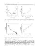
Based on the results shown above, a change in hierarchical structure based on a model of
Wöhler-siloxene multi-sheet layers separated by an Si-O-Si linkage at elevated pyrolysis
temperatures, followed by exposure to air, is proposed in Fig. 12.
2.4 Circularly polarized light from chiral SNPs
The generation, amplification, and switching of circularly polarized luminescence (CPL) and
circular dichroism (CD) by polymers (Chen et al., 1999; Oda et al., 2000; Kawagoe et al.,
2010), small molecules (Lunkley et al., 2008; Harada et al., 2009), and solid surface crystals
(Furumi and Sakka, 2006; Krause & Brett, 2008; Iba et al., 2011) have received considerable
theoretical and experimental attention.
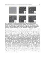
Scheme 5. Soluble, optically-active SNPs bearing chiral organic groups.
Fig. 13. UV-visible, PL, CD, and CPL spectra of 1S, 2S, and 2R in THF at 25 °C.
CPL is inherent to asymmetric luminophores in the excited state, whereas CD is due to
asymmetric chromophores in the ground state. The first chiroptical (CPL and CD) properties
of three new SNPs bearing chiral alkyl side groups (Fukao & Fujiki, 2009) were recently
demonstrated for poly[(S)-2-methylbutylsilyne] (1S), poly[(R)-3,7-dimethyloctylsilyne] (2R),
and poly[(S)-3,7-dimethyloctylsilyne] (2S) (Scheme 5).
Amorphous and Crystalline Silicon Films from Soluble Si-Si Network Polymers
15
This study revealed that only 1S, bearing β-branched chiral groups, clearly showed an
intense CPL signal at ~570 nm with
F
of ~1% along with corresponding Cotton CD signals
in THF solution at room temperature (Fig. 13). In contrast, 2R and 2S, which possess γ-
branched chiral groups, did not exhibit any CPL signals although they did exhibit CD
bands. By analogy to the optically inactive SNPs described above, optically active SNPs
might be candidates for use as Si-source materials in the production of a-Si and c-Si films
that exhibit circular polarization via controlled vacuum pyrolysis.
2.5 A Ge–Ge bonded network polymer (GNP) as an SNP analogue
Our understanding of the Si-Si bonded network polymeric materials led us to investigate a
2D Ge–Ge bonded network polymer (GNP) as a soluble model of insoluble polygermyne. A
common approach for studying Si- and Ge-based materials is to effectively confine a
photoexcited electron-hole pair within the Bohr radius (r
B
) for Si (r
B
~5 nm) and for Ge
(r
B
~24 nm) (Gu et al., 2001). However, research on low-dimensional Ge-based materials has
been delayed due to the limited synthetic approaches available for preparing soluble Ge–Ge
bonded materials using organogermanium sources, which are 1000 times more expensive
than the corresponding organosilane sources. Several Ge-based materials were recently
fabricated using the molecular beam epitaxy (MBE) technique in an ultrahigh vacuum using
inexpensive Ge-based inorganic sources, rapidly increasing their potential use in the fields
of physics and applied physics.
In the area of solid-state physics, Kanemitsu, Masumoto, and coworkers observed a broad
PL band at 570 nm (2.18 eV) for microcrystalline Ge (
c-Ge) embedded into SiO
2
glass at
room temperature (Maeda et al., 1991). Stutzmann, Brandt, and coworkers reported a near
infrared PL band at 920 nm (1.35 eV) for multi-layered Ge sheets produced on a solid
surface, which is a pseudo-2D multi-layered Ge crystal known as polygermyne synthesized
from Zintl-phase CaGe
2
(Vogg et al., 2000). However,
c-Ge, polygermyne, and polysiloxene
are purely inorganic and are thus insoluble in any organic solvent.
Scheme 6. Synthesis of soluble n-butyl GNP.
In 1993, Bianconi et al. reported the first synthesis of GNP via reduction of
n-hexyltrichlorogermane with a NaK alloy under ultrasonic irradiation (Hymanclki et al.,
1993). However, the photophysical properties of GNP have not yet been reported in detail.
In 1994, Kishida et al. reported that poly(n-hexylgermyne) at 77 K possesses a green PL band
with a maximum at 560 nm (2.21 eV) whereas poly(n-hexylsilyne) exhibits a blue PL band
around 480 nm (2.58 eV) (Kishida et al., 1994).
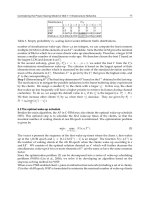
By applying our modified technique to a soluble GNP bearing n-butyl groups (n-BGNP) and
through careful polymer synthesis (Scheme 6) and measurement of the PL, we briefly
demonstrated that n-BGNP exhibits a very brilliant red PL band at 690 nm (1.80 eV). This
result was obtained using a vacuum at 77 K without the pyrolysis process; under these
Crystalline Silicon – Properties and Uses
16
conditions, n-BSNP reveals a very brilliant green-colored PL band at 540 nm (2.30 eV) (Fig.
14) (Fujiki et al., 2009). This result differs from that of a previous report of green PL from
poly(n-hexylgermyne) (Kishida et al., 1994).
Fig. 14. Photographs (left) and PL spectra (right) of n-BSNP and n-BGNP films excited at 365
nm at 77 K.
By analogy with the SNPs described above,
GNP may have potential uses as NIR emitters
and narrow band gap materials with a loss of organic moieties by the pyrolysis process. In
recent years, several studies have demonstrated the preparation and characterization of
Ge nanoclusters capped with organic groups. Watanabe et al. elucidated that pyrolysis
products of soluble Ge-Ge bonded nanoclusters capped with organic groups offer high-
carrier mobility and optical waveguide with a high-refractive index value in
semiconducting materials (Watanabe et al., 2005). Klimov et al. recently reported the
presence of a near IR PL band at 1050 nm (1.18 eV) with a fairly high
F
of 8% for nc-Ge
capped with 1-octadecene, enabling a great reduction in Ge surface oxidation due to
formation of strong Si–C bonds (Lee et al., 2009). The study of GNP pyrolysis is in
progress and will be reported in the future.
2.6 Scope and perspectives
In recent years, solution processes for the fabrication of electronic and optoelectronic
devices, as alternative methods to the conventional vacuum and vapor phase deposition
processes, have received significant attention in a wide range of applications due to their
many advantages, including processing simplicity, reduction in total production costs,
and safety of chemical treatments. Particularly, the utilization of liquefied source material
of an air-stable, non-toxic, non-flammable, non-explosive solid may be essential in some
potential applications in printed semiconductor devices for large-area flexible displays,
solar cells, and thin-film transistors (TFTs). Recent progress in this area has largely been
focused on organic semiconductors with -conjugated polymers due to their ease of
processing, some of which have a relatively high carrier mobility that is comparable to
that of a-Si.
Because of their ease of coating and dispersion in the form of ‘Si-ink’ in comparison to II-VI
group nanocrystals [Colvin et al., 1994], soluble SNP, GNP, and their pyrolysis products can
serve as Si-/Ge-source materials for the production of variable range Si-based and/or Si-Ge
alloyed semiconductors at room temperature. The ionization potential of the pyrolyzed Si
materials range between 5.2 and 5.4 eV while the electron affinity ranges between 4.0 and
3.2 eV (Lu et al., 1995). These values are well-matched with the work-functions of ITO and
Amorphous and Crystalline Silicon Films from Soluble Si-Si Network Polymers
17
Al/Ag/Mg electrodes. Recently, air stable red-green-blue emitting nc-Si was achieved using
a SiH
4
plasma following CF
4
plasma etching (Pi et al., 2008). As an alternative method, laser
ablation of bulk c-Si in supercritical CO
2
after excitation with a 532-nm nanosecond pulsed
laser yielded nc-Si that could produce blue, green, and red emitters. (Saitow & Yamamura,
2009). As we have demonstrated, controlled vacuum pyrolysis using a single SNP source
material, possibly including GNP source material, should offer a new, environmentally
friendly, safer process to efficiently produce red-green-blue-near infrared emitters, thin
films for TFTs, and solar cells because the required technology is largely compatible with
XeCl excimer laser annealing and the crystallization process for making poly-Si TFTs from a-
Si thin films deposited using the SiH
4
–Si
2
H
6
CVD process.
The dimensionality of inorganic materials makes it possible to tailor the band gap value, as
shown in Table 1. Soluble SNP and GNP, because of their ease of coating and dispersion in
the form of "Si-ink" and "Ge-ink", may serve as controlled soluble Si/Ge source materials
without the need for the SiH
4
/GeH
4
CVD process. Our results provide a better
understanding of the intrinsic nature of pseudo-2D Si electronic structure by varying Si
layer numbers. The chemistry of SNP vacuum pyrolysis opens a new methodology to safely
produce a-Si, c-Si, Si-based semiconductors, and alloys with Ge.
3. Summary
Although c-Si is the most archetypal semiconducting material for microelectronics, it is a
poor visible emitter with a quantum yield of 0.01% at 300 K and a long PL lifetime of several
hours. Pyrolysis of chain-like Si-containing polysilane and polycarbosilane has previously
been shown to efficiently produce
-SiC; however, our TGA and ITGA pyrolysis
experiments with various soluble SNPs indicated that elemental Si is produced. The SNP
was transformed into a visible emitter that is tunable from 460 nm (2.7 eV) to 740 nm (1.68
eV) through control of the pyrolysis temperature and time (200–500 °C, 10-90 min).
Moreover, air-exposed nc-like-Si, produced by pyrolyzing SNP at 500 °C, showed an intense
blue PL with a maximum at 430 nm, a quantum yield of 20–25%, and a short lifetime of ~5
nsec; furthermore, these particles disperse in common organic solvents at room
temperature. HRTEM, laser-Raman, and second-derivative UV-visible, PL, and PLE spectra
indicated that the siloxene-like, multi-layered Si-sheet structures are responsible for the
wide range of visible PL colors with high quantum yields. Circular polarization for SNPs
bearing chiral side groups was also demonstrated for the first time. Through an analogous
synthesis to that of green photoluminescent SNPs, the Ge-Ge bonded network polymer,
GNP, was determined to be a red photoluminescent material.
4. Acknowledgements
This work was fully supported by the Nippon Sheet Glass Foundation for Materials Science
and Engineering and partially supported by a Grant-in-Aid for Scientific Research (B) from
MEXT (22350052, FY2010–FY2013). The authors thank Prof. Kyozaburo Takeda, Prof. Kenji
Shiraishi, Prof. Nobuo Matsumoto, Prof. Masaie Fujino, Prof. Akira Watanabe, Prof.
Masanobu Naito, Prof. Kotohiro Nomura, Prof. Akiharu Satake, Dr. Kazuaki Furukawa, Dr.
Anubhav Saxena, and our students, Dr. Masaaki Ishikawa, Satoshi Fukao, Dr. Takuma
Kawabe, Yoshiki Kawamoto, Masahiko Kato, Yuji Fujimoto, Tomoki Saito, and Shin-ichi
Hososhima for their helpful discussions and contributions.
Crystalline Silicon – Properties and Uses
18
5. References
Alivisatos, A. P. (1996). Perspectives on the physical chemistry of semiconductor
nanocrystals. The Journal of Physical Chemistry, Vol. 100, No. 31, 13226-13239.
Bianconi, P. A.; Schilling, F. C. & Weidman, T. W. (1989). Ultrasound-mediated reductive
condensation synthesis of silicon-silicon-bonded network polymers.
Macromolecules, Vol. 22, No. 4, 1697–1704.
Bianconi, P. A. & Weidman, T. W. (1988). Poly(n-hexylsilyne): Synthesis and properties of
the first alkyl silicon [RSi]
n
network polymer. Journal of the American Chemical
Society, 1988, Vol. 110, No. 7, 2342–2344.
Brus, L. (1994). Luminescence of silicon materials: chains, sheets, nanocrystals, nanowires,
microcrystals, and porous silicon. The Journal of Physical Chemistry, Vol. 98, No. 14,
3575–3581.
Bley, R. A. & Kauzlarich, S. M. (1996). A low-temperature solution phase route for the
synthesis of silicon nanoclusters. Journal of the American Chemical Society, Vol. 118,
No. 49, 12461–12462.
Brandt, M. S.; Vogg, G. & Stutzmann, M. (2003). Silicon- and Germanium-Based Sheet Polymers
and Zintl Phases, in Jutzi, P. & Schubert, U. (eds.), Silicon Chemistry, ISBN-13: 978-
3527306473, Wiley-VCH, Weinheim, Chapter 15, pp. 194–213.
Chen, S. H., Katsis, D., Schmid, A. W., Mastrangelo, J. C., Tsutsui, T. & Blanton, T. N. (1999).
Circularly polarized light generated by photoexcitation of luminophores in glassy
liquid-crystal films. Nature, Vol. 397, 11 February 1999, 506–508.
Choi, J.; Wang, N. S. & Reipa, V. (2007). Photoassisted tuning of silicon nanocrystal
photoluminescence. Langmuir, Vol. 23, No. 6, 3388–3394.
Colvin, V. L.; Schlamp, M. C. & Alivisatos, A. P. (1994). Light-emitting diodes made from
cadmium selenide nanocrystals and a semiconducting polymer, Nature, Vol. 370, 4
August 1994, 354–357.
Cullis, A. G. & Canham, L. T. (1991). Visible light emission due to quantum size effects in
highly porous crystalline silicon. Nature, Vol. 353, 26 September 1991, 335–338.
Cullis, A. G.; Canham, L. T. & Calcott, P. E. J. (1997). The structural and luminescence
properties of porous silicon. Journal of Applied Physics, Vol. 82, No. 3, 909–965.
Davies, J. H. (1998). The Physics of Low-dimensional Semiconductors: An Introduction, ISBN-13:
978-0521484916, Cambridge University Press, Cambridge.
Diener, J.; Kovalev, D.; Koch, F. & Tsybeskov, L. Ordering and self-organization in
nanocrystalline silicon. Nature 2000, Vol. 407, 21 September 2000, 358–361.
English, D. S.; Pell, L. E.; Yu, Z.; Barbara, P. F. & Korgel, B. A. (2002). Size tunable visible
luminescence from individual organic monolayer stabilized silicon nanocrystal
quantum dots. Nano Letters Vol. 2, No. 7, 681-685.
Fujiki, M. (2001). Optically active polysilylenes: State-of-the-art chiroptical polymers.
Macromolecular Rapid Communications, Vol. 22, No. 8, 539–563.
Fujiki, M.; Kawamoto, Y.; Kato, M.; Fujimoto, Y.; Saito, T.; Hososhima, S i. & Kwak, G.
(2009). Full-visible-spectrum emitters from pyrolysis of soluble Si-Si bonded
network polymers. Chemistry of Materials, Vol. 21, No. 12, 2459–2466.
Fujiki, M.; Kato, M.; Kawamoto, Y. & Kwak, G. (2011). Green-and-red photoluminescence
from Si–Si and Ge–Ge bonded network homopolymers and copolymers. Polymer
Chemistry, Vol. 2, No. 4, 914–922.
Amorphous and Crystalline Silicon Films from Soluble Si-Si Network Polymers
19
Fojtik, A. & Henglein, A. (1994). Luminescent colloidal silicon particles. Chemical Physics
Letters, Vol. 221, No. 5–6, 363–367.
Fukao, S. & Fujiki, M. (2009). Circularly polarized luminescence and circular dichroism from
Si-Si-bonded network polymers. Macromolecules, Vol. 42, No. 21, 8062–8067.
Furukawa, K.; Fujino, M. & Matsumoto, N. (1990). Optical properties of silicon network
polymers. Macromolecules, Vol. 23, No. 14, 3423–3426.
Furukawa, K. (2000). Synthesis and Optical Properties of Silicon-backbone Materials: (RSi)n (R =
Organic group), Doctor thesis, Waseda University, Tokyo, Japan, Chapter 7 (in
Japanese).
Furukawa, S. & Miyasato, T. (1988). Quantum size effects on the optical band-gap of
microcrystalline Si-H. Physical Review B, Vol. 38, No. 8, 5726–5729.
Furumi, S. & Sakka, Y. (2006). Chiroptical properties induced in chiral photonic-bandgap
liquid crystals leading to a highly efficient laser-feedback effect. Advanced Materials,
Vol. 18, No. 6, 775–780.
Gelloz, B.; Kojima, A. & Koshida, N. (2005). Highly efficient and stable luminescence of
nanocrystalline porous silicon treated by high-pressure water vapor annealing.
Applied Physics Letters, Vo. 87, No. 3, 031107.
Gu, G.; Burghard, M.; Kim, G. T.; Düsberg, G. S.; Chiu, P. W.; Krstic, V.; Roth S. & Han, W.
Q. (2001). Growth and electrical transport of germanium nanowires. Journal of
Applied Physics, 2001, Vol. 90, No. 11, 5747–5751.
Harada, T., Nakano, Y., Fujiki, M., Naito, M., Kawai, T. & Hasegawa, Y. (2009). Circularly
polarized luminescence of Eu(III) complexes with point- and axis-chiral ligands
dependent on coordination structures. Inorganic Chemistry, Vol. 48, No. 23, 11242–
11250.
Hasegawa, T.; Iwasa, Y.; Koda, T.; Kishida, H.; Tokura, Y.; Wada, S.; Tashiro, H.; Tachibana,
H. & Matsumoto, M. (1996). Nature of one-dimensional excitons in polysilanes.
Physical Review B, Vol. 54, No. 16, 11365–11374.
Heitmann, J.; Möller, F.; Zacharias, M. & Gösele, U. (2005). Silicon nanocrystals: size matters.
Advanced Materials, Vol. 17, No. 7, 795–803.
Holmes, J. D.; Ziegler, K. J.; Doty, R. C.; Pell, L. E.; Johnston, K. P. & Korgel, B. A. (2001).
Highly luminescent silicon nanocrystals with discrete optical transitions. Journal of
the American Chemical Society, Vol. 123, No. 16, 3743–3748.
Hua, F.; Erogbogbo, F.; Swihart, M. T. & Ruckenstein, E. (2006). Organically capped silicon
nanoparticles with blue photoluminescence prepared by hydrosilylation followed
by oxidation. Langmuir, Vol. 22, No. 9, 4363–4370.
Hymanclki, W. J.; Viclscher, G. T. & Bianconi, P. A. (1993). Polygermynes: Synthesis and
properties of germanium-germanium bonded network polymers. Macromolecules,
1993, Vol. 26, No. 4, 869–871.
Iba, S., Koh, S., Ikeda, K. & Kawaguchi, H. (2011). Room temperature circularly polarized
lasing in an optically spin injected vertical-cavity surface-emitting laser with (110)
GaAs quantum wells. Applied Physics Letters, Vol. 98, No. 8, 081113 (2011).
Jurbergs, D.; Rogojina, E.; Mangolini, L. & Kortshagen, U. (2006). Silicon nanocrystals with
ensemble quantum yields exceeding 60%. Applied Physics Letters, Vol. 88, No. 23,
233116.
Crystalline Silicon – Properties and Uses
20
Kanemitsu, Y.; Ogawa, T.; Shiraishi, K. & Takeda, K. (1993). Visible photoluminescence from
oxide Si nanometer-sized spheres - Exciton confinement on a spherical-shell.
Physical Review B, Vol. 48, No. 7, 4883–4886.
Kanemitsu, Y. (1996). Photoluminescence spectrum and dynamics in oxidized silicon
nanocrystals: A nanoscopic disorder system. Physical Review B, Vol. 53, No. 20,
13515–13520.
Kawagoe, Y., Fujiki, M. & Nakano, Y. (2000). Limonene magic: noncovalent molecular
chirality transfer leading to ambidextrous circularly polarised luminescent π-
conjugated polymers. New Journal of Chemistry, Vol. 34, No. 4, 637–647.
Kishida, H.; Tachibana, H.; Matsumoto, M. & Tokura, Y. (1994). Optical spectra of Si/Ge-
network copolymers: [Si(C
6
H
13
)]
1-x
[Ge(C
6
H
13
)]
x
. Applied Physics Letters, 1994, Vol. 65,
No. 11, 1358–1360.
Kovalev, D.; Heckler, H.; Ben-Chorin, M.; Polisski, G.; Schwartzkopff, M. & Koch, F. (1998).
Breakdown of the k-conservation rule in Si nanocrystals. Physical Review Letters,
Vol. 81, No. 13, 2803-2806.
Kovalev, D. & Fujii, M. (2005). Silicon nanocrystals: photosensitizers for oxygen molecules.
Advanced Materials, Vol. 17, No. 21, 2531–2544.
Konagai, M. (1987). Handotai Chokoshi Nyumon (Introduction to Semiconductor Superlattice),
ISBN-13: 978-4563034351, Baifukan, Tokyo (in Japanese).
Krause, K. M. & Brett, M. J. (2008). Spatially graded nanostructured chiral films as tunable
circular polarizers. Advanced Functional Materials, Vol. 18, No. 20, 3111–3118.
Lee, D. C.; Pietryga, J. M.; Robel, I.; Werder, D. J.; Schaller, R. D. & Klimov, V. I. (2009).
Colloidal synthesis of infrared-emitting germanium nanocrystals. Journal of the
American Chemical Society, Vol. 131, No. 10, 3436–3437.
Lehmann, V. & Gösele, U. (1991). The structural and luminescence properties of porous
silicon. Applied Physics Letters, Vol. 58, No. 8, 856–858.
Li, X.; He, Y. & Swihart, M. T. (2004). Surface functionalization of silicon nanoparticles
produced by laser-driven pyrolysis of silane followed by HF-HNO
3
etching.
Langmuir, Vol. 20, No. 11, 4720–4727.
Liu, Q.; Wu, H J.; Lewis, R.; Maciel, G. E. & Interrante, L. V. (1999). Investigation of the
pyrolytic conversion of poly(silylenemethylene) to silicon carbide. Chemistry of
Materials, Vol. 11, No. 8, 2038–2048.
Liu, S M. (2008). Luminescent silicon nanoparticles formed in solution. Journal of
Nanoscience and Nanotechnology, Vol. 8, No. 3, 1110–1125.
Liu, S M.; Sato, S. & Kimura, K. (2005). Synthesis of luminescent silicon nanopowders
redispersible to various solvents. Langmuir, Vol. 21, No. 14, 6324–6329.
Liu, S M.; Yang, Y.; Sato, S. & Kimura, K. (2006). Enhanced photoluminescence from Si
nano-organosols by functionalization with alkenes and their size evolution.
Chemistry of Materials, Vol. 18, No. 3, 637–642.
Lockwood, D. J. (1998). Light Emission in Silicon, in Lockwood, D. J. (ed.), Light Emission in
Silicon From Physics to Devices, Academic Press, ISBN-13: 978-0127521572, New
York, 1998. Chapter 1, pp 1–34.
Lu, Z. H.; Lockwood, D. J. & Baribeau, J M. (1995). Quantum confinement and light
emission in SiO
2
/Si superlattices. Nature, Vol. 378, 16 November 1995, 258–260.
Lunkley, J. L., Shirotani, D., Yamanari, K., Kaizaki, S. & Muller, G. (2008). Extraordinary
circularly polarized luminescence activity exhibited by cesium tetrakis(3-
Amorphous and Crystalline Silicon Films from Soluble Si-Si Network Polymers
21
heptafluoro-butylryl-(+)-camphorato) Eu(III) complexes in EtOH and CHCl
3
Solutions. Journal of the American Chemical Society, Vol. 130, No. 42, 13814–13815.
Maeda, Y.; Tsukamoto, N.; Yazawa, Y.;Kanemitsu, Y. & Masumoto, Y. (1991). Visible
photoluminescence of Ge microcrystals embedded in SiO
2
glassy matrices. Applied
Physics Letters, 1991, Vol 59, No. 24, 3168–3170.
Ma, D. D. D.; Lea, S. T. & Shinar, J. (2005). Strong polarization-dependent photolumine-
scence from silicon nanowire fibers. Applied Physics Letters, Vol. 87, No. 3, 033107.
Martin, H P.; Müller, E.; Richter, R.; Roewer, G. & Brendler, E. (1997). Methyl-
chlorooligosilanes as products of the basecatalysed disproportionation of various
methylchlorodisilanes. Journal of Organometallic Chemistry, Vol. 32, No. 1381–1387.
Mayeri, D.; Phillips, B. L.; Augustine, M. P. & Kauzlarich, S. M. (2001). NMR study of the
synthesis of alkyl-terminated silicon nanoparticles from the reaction of SiCl
4
with
the Zintl salt, NaSi. Chemistry of Materials. Vol. 13, No. 3, 765–770.
Nayfeh, M. & Mitas, L. (2008). Silicon Nanoparticles: New Photonic and Electronic Material at the
Transition Between Solid and Molecules, in Kumar, V. (ed.), Nanosilicon, Elsevier,
Oxford, ISBN-13: 978-0080445281, Chapter 1, pp. 1–78.
Nesper, R. (2003). Structural and Electrnic Systematics in Zintl Phases of the Tetrels, in Jutzi, P. &
Schubert, U. (eds.), Silicon Chemistry, ISBN-13: 978-3527306473, Wiley-VCH,
Weinheim, Chapter 13, pp. 171–180.
Oda, M.; Nothofer, H.G.; Lieser, G.; Scherf, U.; Meskers, S. C. & Neher, D. (2000). Circularly
polarized electroluminescence from liquid-crystalline chiral polyfluorenes.
Advanced Materials, Vol. 12, No. 5, 362-365.
Pi, X. D.; Liptak, R. W.; Nowak, J. D.; Wells, N. P.; Carter, C. B.; Campbell, S. A. &
Kortshage, U. (2008). Air-stable full-visible-spectrum emission from silicon
nanocrystals synthesized by an all-gas-phase plasma approach. Nanotechnology,
Vol. 19, No. 24, 245603.
Qi, J.; Belcher, A. M. & White, J. M. (2003). Spectroscopy of individual silicon nanowires.
Applied Physics Letters, Vol. 82, No. 16, 2616–2618.
Saitow, K. & Yamamura, T. (2009). Effective cooling generates efficient rmission: Blue, green,
and red light-emitting Si nanocrystals. The Journal of Physical Chemistry C, Vol. 113,
No. 19, 8465–8470.
Schmidt, W. R.; Interrante, L. V.; Doremus, R. H.; Trout, T. K.; Marchetti, P. S. & Maciels, G.
E. (1991). Pyrolysis chemistry of an organometallic precursor to silicon carbide.
Chemistry of Materials, Vol. 3, No. 2, 257–267.
Shimoda, T.; Matsuki, Y.; Furusawa, M.; Aoki, T.; Yudasaka, I.; Tanaka, H.; Iwasawa, H.;
Wang, D.; Miyasaka, M. & Takeuchi, Y. Solution-processed silicon films and
transistors. Nature 2006, Vol. 440, 6 April 2006, 783–786.
Shini, K. & Kumada, M. (1958). Thermal rearrangement of hexamethyldisilane to trimethyl-
(dimethylsilylmethyl)silane. The Journal of Organic Chemistry, Vol. 23, No. 1, 139-
139.
Smith, D. A.; Joray, S. J. & Bianconi, P. A. (2005). Synthetic method development and
molecular weight control for homo- and co-polysilynes, silicon-based network-
backbone polymers. Journal of Polymer Research, 2005, Vol. 12, No. 5, 393–401.
Takagi, H.; Ogawa, H.; Yamazaki, A.; Ishizaki, A. & Nakagiri, T. (1990). Quantum size
effects on photoluminescence in ultrafine Si particles. Applied Physics Letters, Vol.
56, No. 24, 2379–2381.
Crystalline Silicon – Properties and Uses
22
Takeda, K.; Teramae, H. & Matsumoto, N. (1986). Electronic structure of chainlike
polysilane. Journal of the American Chemical Society, Vol. 108, No. 26, 8186–8190.
Takeda, K. & Shiraishi, K. (1989). Electronic structure of Si-skeleton materials. Physical
Review B, Vol. 39, No. 15, 11028–11037.
Takeda, K. & Shiraishi, K. (1993). Electronic structure of silicon-oxygen high polymers. Solid
State Communications, Vol. 85, No. 4, 301–305.
Teramae, H. & Takeda, K. (1989). Ab initio studies on silicon compounds. Part II. The
gauche structure of the parent polysilane. Journal of the American Chemical Society,
Vol. 111, No. 4, 1281–1285.
Vogg, G.; Brandt, M. S. & Stutzmann, M. (2000). Polygermyne—A prototype system for
layered germanium polymers. Advanced Materials, 2000, Vol. 12, No. 17, 1278–1281.
Walters, R. J.; Kalkman, J.; Polman, A.; Atwater, H. A. & de Dood, M. J. A. (2006).
Photoluminescence quantum efficiency of dense silicon nanocrystal ensembles in
SiO
2
. Physical Review B, Vol. 73, No. 13, 132302.
Watanabe, A. (2003). Optical properties of polysilanes with various silicon skeletons. Journal
of Organometallic Chemistry, Vol. 685, No. 1-2, 122–133.
Watanabe, A.; Hojo, F. & Miwa, T. (2005). Field-effect transistor based on organosoluble
germanium nanoclusters. Applied Organometallic Chemistry, Vol. 19, No. 4, 530–537.
Wilcoxon, J. P.; Samara, G. A. & Provencio, P. N. (1999). Optical and electronic properties of
Si nanoclusters synthesized in inverse micelles. Physical Review B, Vol. 60, No. 4,
2704–2714.
Wilson, W. L. & Weidman, T. W. (1991). Excited-state dynamics of one- and two-
dimensional σ-conjugated silicon frame polymers: dramatic effects of branching in
a series of hexylsilyne-branched poly(hexylmethylsilylene) copolymers. The Journal
of Physical Chemistry, Vol. 95, No. 11, 4568–4572.
Wilson, W. L.; Szajowski, P. F. & Brus, L. E. (1993). Quantum confinement in size-selected,
surface-oxidized silicon nanocrystals. Science, Vol. 262, No. 5137, 1242–1244.
Yu, P. Y. & Cardona, M. (2005). Fundamentals of Semiconductors: Physics and Materials
Properties; 3rd Ed., Springer-Verlag, ISBN-13: 978-3540254706, Chapter 7, 345–426.
Yajima, S.; Hasegawa, Y.; Hayashi, J. & Iimura, M. (1978). Synthesis of continuous silicon
carbide fibre with high tensile strength and high Young's modulus: Part 1.
Synthesis of polycarbosilane as precursor. Journal of Material Science, Vol. 13, No. 12,
2569–2576.
Zou,J.; Baldwin, R. K.; Pettigrew, K. A. & Kauzlarich, S. M. (2004). Solution synthesis of
ultrastable luminescent siloxane-coated silicon nanoparticles. Nano Letters, Vol. 4,
No. 7, 1181–1186.
Zhang, X.; Brynda, M.; Britt, R. D.; Carroll, E. C.; Larsen, D. S.; Louie, A. Y. & Kauzlarich, S.
M. (2007). Synthesis and characterization of manganese-doped silicon
nanoparticles: Bifunctional paramagnetic-optical nanomaterial. Journal of the
American Chemical Society, Vol. 129, No. 35, 10668–10669.
2
Study of SiO
2
/Si Interface
by Surface Techniques
Constantin Logofatu, Catalin Constantin Negrila,
Rodica V. Ghita, Florica Ungureanu, Constantin Cotirlan,
Cornelui Ghica Adrian Stefan Manea and Mihai Florin Lazarescu
National Institute of Materials Physics, Bucharest
Romania
1. Introduction
Due to its dominant role in silicon devices technologies [1, 2] the SiO
2
/Si interface has been
intensively studied in the last five decades. The ability to form a chemically stable protective
layer of silicon dioxide (SiO
2
) at the surface of silicon is one of the main reasons that make
silicon the most widely used semiconductor material. This silicon oxide layer is a high
quality electrically insulating layer on the silicon surface, serving as a dielectric in numerous
devices that can also be a preferential masking layer in many steps during device
fabrication. Native oxidation of silicon is known to have detrimental effects on ultra-large-
scale integrated circuit (ULSIC) processes and properties including metal/silicon ohmic
contact, the low-temperature epitaxy of silicide and dielectric breakdown of thin SiO
2
[3].
The use of thermal oxidation of Si(100) to grow very thin SiO
2
layers (~ 100Ǻ) with
extremely high electrical quality of both film and interface is a key element on which has
been built the success of modern MOS (metal-oxide-semiconductor) device technology [4].
At the same time the understanding of the underlying chemical and physical mechanisms
responsible for such perfect structures represents a profound fundamental challenge, one
which has a particular scientific significance in that the materials (Si, O) and chemical
reaction processes (e.g. thermal oxidation and annealing) are so simple conceptually.
As a result of extreme decrease in the dimensions of Si metal-oxide-semiconductor field
effect transistor device (MOSFET), the electronic states in Si/SiO interfacial transition region
playa vital role in device operation [5]. The existence of abrupt interfaces, atomic
displacements of interface silicon and intermediate oxidation states of silicon are part of
different experiments [6, 7]. The chemical bonding configurations deduced from the
observed oxidation states of silicon at the interface are the important basis for the
understanding of the electronic states. The distribution of the intermediate oxidation states
in the oxide film and the chemical bonding configuration at the interface for Si(100) and
Si(111) were investigated [5] using measurements of Si 2p photoelectron spectra. One of the
X-ray photoelectron spectroscopy (XPS) results is that the difference for <100> and <111>
orientations is observed in the intermediate oxidation state spectra. Ultra thin SiO
2
films are
critical for novel nanoelectronic devices as well as for conventional deep submicron ULSIC
where the gate oxide is reduced to less than 30Ǻ. Precise thickness measurement of these
Crystalline Silicon – Properties and Uses
24
ultra thin films is very critical in the development of Si- based devices. Oxide thickness is
commonly measured by ellipsometry [8] but as film thicknesses is scaled down to several
atomic layers, surface analytical techniques such as XPS become applicable tools to quantify
these films [9]. An XPS measurement offers the additional advantage of providing
information such as surface contamination and chemical composition of the film.
The purpose of the present section is to study the chemical structure modifications at the
surface on semiconductors (e.g. Si, GaAs) by XPS, (angle resolved XPS) ARXPS and (scanning
tunneling microscopy) STM techniques. It will be studied the variation of the interface for
native oxides and for thermally grown oxides. This analysis will be the base for in situ
procedures in the development of different devices as Schottky diodes or in the technique of
local anodic oxidation (LAO) [10] for fabricating electronic devices on a nanometer scale.
A silicon dioxide layer is often thermally formed in the presence of oxygen compounds at a
temperature in the range 900 to 1300
0
C. There exist two basic means of supplying the
necessary oxygen into the reaction chamber. The first is in gaseous pure oxygen form (dry
oxidation) through the reaction: Si+O
2
→SiO
2
. The second is in the form of water vapor (wet
oxidation) through the reaction: Si+2H
2
O→SiO
2
+2H
2
. For both means of oxidation, the high
temperature allows the oxygen to diffuse easily through the silicon dioxide and the silicon is
consumed as the oxide grows. A typical oxidation growth cycle consists of dry-wet-dry
oxidations, where most of the oxide is grown in the wet oxidation phase. Dry oxidation is
slower and results in more dense, higher quality oxides. This type of oxidation method is
used mostly for MOS gate oxides. Wet oxidation results in much more rapid growth and is
used mostly for thicker masking layers. Before thermal oxidation, the silicon is usually
preceded by a cleaning sequence designed to remove all contaminants. Sodium
contamination is the most harmful and can be reduced by incorporating a small percentage
of chlorine into the oxidizing gas. The cleaned wafers are dried and loaded into a quartz
wafer holder and introduced in a furnace. The furnace is suitable for either dry or wet
oxidation film growth by turning a control valve. In the dry oxidation method, oxygen gas is
introduced into the quartz tube. High-purity gas is used to ensure that no impurities are
incorporated in the oxide layer as it forms. The oxygen gas can also be mixed with pure
nitrogen in order to decrease the total cost of oxidation process. In the wet oxidation
method, the water vapor introduced into the furnace system is usually creating by passage a
carrier gas into a container with ultra pure water and maintained at a constant temperature
below its boiling point (100
0
C). The carrier gas can be either nitrogen or oxygen and both
result in equivalent oxide thickness growth rates.
The structure of SiO
2
/Si interface has been elusive despite many efforts to come up with
models. Previous studies [11-13] generally agree in identifying two distinct regions. The
near interface consists of a few atomic layers containing Si atoms in intermediate oxidation
states i.e. Si
1+
(Si
2
O), Si
2+
(SiO) and Si
3+
(Si
2
O
3
). A second region extends about 30Ǻ into SiO
2
overlayer. The SiO
2
in this layer is compressed because the density of Si atoms is higher for
Si than for SiO
2
. Different structural models [14-17] have been proposed for SiO
2
on Si (100),
each predicting a characteristic distribution of oxidation states, and most of the models
assume an atomically abrupt interface. From experiments was observed [1] at interface the
existence of a large portion of Si
3+
, and the model in accord this observation is that of an
extended-interface for SiO
2
/Si (100) by minimizing the strain energy [17]. Relatively new
models (’90 years) are based for SiO
2
/Si (100) and SiO
2
/Si (111) on the distribution and
intensity of intermediate oxidation states. These models are characterized by an extended
interface with protrusions of Si
3+
reaching about 3 Ǻ into the SiO
2
overlayer.
Study of SiO
2
/Si Interface by Surface Techniques
25
Experimental techniques as the one presented in this work were used to determine the
structure of the interface, its extend and to appreciate its roughness.
2. Investigation techniques
X-ray Photoelectron Spectroscopy (XPS) technique offers several key features which makes it
ideal for structural and morphological characterization of ultra-thin oxide films. The relatively
low kinetic energy of photoelectrons (< 1.5 keV) makes XPS inherently surface sensitive in
the range (1-10 nm). Secondly, the energy of the photoelectron is not only characteristic of
the atom from which it was ejected, but also in many cases is characteristic of the
oxidation state of the atom (as an example the electrons emitted from 2p
3/2
shell in SiO
2
are present approximately 4 eV higher in binding energy than electrons from the same
shell originating from Si
0
(bulk Si). In the third place the XPS has the advantage that is
straightforward to quantify through the use of relative sensitivity factors that are largely
independent of the matrix.
The XPS recorded spectra were obtained using SPECS XPS spectrometer based on Phoibus
analyzer with monochromatic X-rays emitted by an anti-cathode of Al (1486.7 eV). The
complex system of SPECS spectrometer presented in Fig.1 allows the ARXPS analysis, UPS
and STM as surface investigation techniques.
Fig. 1. SPECS complex system for surface analysis
Crystalline Silicon – Properties and Uses
26
A hemispherical analyzer was operated in constant energy mode with a pass energy of 5 eV
giving an energy resolution of 0.4 eV, which was established as FWHM (full width half
maximum) of the Ag 3d5/2 peak. The analysis chamber was maintained in ultra high
vacuum conditions (~ 10
-9
torr). As a standard practice in some XPS studies the C (1s) line
(285 eV) corresponding to the C-C line bond had been used as reference Binding Energy
(BE) [18]. The recorded XPS spectra were processed using Spectral Data Procesor v 2.3 (SDP)
software. In its structure the SDP soft uses the deconvolution of a XPS line as a specific ratio
between Lorentzian and Gaussian line shape and these characteristics ensures a good fit of
experimental data.
Angle resolved X-ray Photoelectron Spectroscopy (ARXPS) is related to a XPS analysis of
recorded spectra on the same surface at different detection angles θ of photoelectrons
measured to the normal at the surface. The analysis chamber is maintained at ultra-high
vacuum (~ 10
-9
torr) and the take-off-angle (TOA) was defined in accord to ASTM document
E 673-03 related to standard terminology related to surface analysis that describes TOA as
the angle at which particles leave a specimen relative to the plane of specimen surface; it is
worth to mention that our experimental measured angle is congruent with TOA as angles
with correspondingly perpendicular sides. For a detection angle θ, the depth λ from where it
proceeds the XPS signal is given by the projection of photoelectrons pass λ
m
(the maximum
escape depth) on the detection direction:
λ= λ
m
cosθ
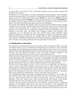
In Fig.2 is presented the TOA angle considered in the equation for oxide thickness
evaluation as presented in [3, 19, 20, and 21].
Fig. 2. Sample characteristics in ARXPS measurement
The oxide film thickness d
oxy
is determined by the Si 2p core level intensity ratio of the
oxidized silicon film I
oxy
and substrate silicon I
si
by:
h
n
X
1
x
e
Study of SiO
2
/Si Interface by Surface Techniques
27
d
oxy
=λ
oxy
sinθ[I
oxy
/(αI
Si
)+1] (1) reference [9]
where
α=I
oxide∞
/I
si∞
= 0.76 (2)
The value for this ratio was experimentally obtained taking into account the intensity for the
line SiO
2
(Si
4+
) in a thick layer of oxide (where the signal for the bulk silicon is not present)
reported to the intensity of Si
0
line in bulk silicon (where the oxide do not exists e.g. after
Ar
+
ion sputtering).
It is well known however that large discrepancies exist for the photoelectron effective
attenuation length in SiO
2
where values from 2 to 4 nm have been reported and compared to
theoretical prediction for the inelastic mean free path. The ARXPS measurements are
dependent on the value of sinθ, and the ratio I
oxy
/I
Si
will be computed only for SiO
2
oxide
(Si
4+
). The electron inelastic mean free path (IMFP) λ is analyzed and computed in terms of
the Bethe equation for inelastic scattering which can be written [22]:
λ=E/ [E
p
2
β ln (γE)] Å (3)
For electrons in the range (50-200) eV [7, 8] the computed IMFP is presented in the form of
TPP-2M formula:
λ=E/ {E
p
2
[βln (γE)-C/E+ D/E
2
]} (4)
E-electron energy (in eV)
β= -0.10+0.944/ (E
p
2
+ E
g
2
) + 0.069 ρ
0.1
γ= 0.191 ρ
-0.50
(5)
C= 1.97- 0.91 U
D= 53.4 – 20.8 U
U = N
V
ρ/ A (N
V
- total number of valence electrons per atom or molecule, ρ- density (gcm
-3
),
A- atomic or molecular weight, E
g
-band gap, E
p
- plasmon energy)
For E
p
which is the free- electron plasmon energy (in eV) it was used the formula
E
p
= 28.8 (ρN
V
/A )
1/2
eV (6)
as is mentioned in reference [21].
For compounds N
V
is calculated from the sum of contributions from each constituent
element (i.e. N
V
for each element multiplied by the chemical or estimated stoichiometric
coefficient for that element) [19].
The explored depth of surface layers by XPS technique can be adjusted by the variation of θ
angle.
Scanning Tunneling Microscopy (STM) is based on the quantum mechanical effect of
tunneling. If two metals are brought in close contact and a small voltage is applied between
them, a tunneling current can be measured which is:
I
t
~ exp (-2kd) (7)
where d is the distance between the conductors, and as an important message the reason
why STM works, is the exponential dependence of the tunneling current on the distance
between conductors. Typical values for tunneling voltage are from few mV to several V, and
Crystalline Silicon – Properties and Uses
28
for the current from 0.5 to 5 nA. The tip-sample distance is a few Angstrom; the tunneling
current depends very strongly on this distance. A change of 1 Å causes a change in the
tunneling current by a factor of ten. In practice, the tunneling voltage is not always very
small. Especially for semiconductors materials a small tunneling voltage can be impossible
because there are no carriers in the gap which can be involved in the tunneling. This means
that STM can look at both, occupied and unoccupied states of the sample depending on the
bias voltage.
Transmission Electron Microscopy (TEM)-is a microscopy technique whereby a beam of
electrons is transmitted through an ultra thin specimen, interacting with the specimen as it
passes through. TEMs are capable of imaging at a significantly higher resolution owing to
the small de Broglie wavelength of electrons. This enables the instrument’s user to examine
fine details-even as small as a single column of atoms. At smaller magnifications TEM image
contrast is due to absorption of electrons in the material, due to the thickness and
composition of the material.
UV-Photoelectron Spectroscopy (UPS)-is the most powerful technique available for probing
surface electronic structure. UPS in the laboratory requires a He gas discharge line source
which can be operated to maximize the output of either He I (21.2 eV) or He II (40.8 eV)
radiation. The use of these photon energies makes accessible only valence levels and very
shallow core levels. UPS refers to the measurement of kinetic energy spectra of
photoelectrons emitted by ultraviolet photons, to determine molecular energy levels in the
valence region [23]. The kinetic energy E
K
of an emitted photoelectron is given by (Einstein
law applied to a free molecule):
E
K
=hν-I (8)
Where h is Planck’s constant, ν is the frequency of the ionizing light, and I is an ionization
energy corresponding to the energy of an occupied molecular orbital. In the study of solid
surfaces in particular is sensitive to the surface region (to 10 nm depth) due to the short
range of the emitted photoelectrons (compared to X-rays). A useful result from
characterization of solids by UPS is the determination of the work function of the material.
The work function Φ can be defined in terms of the minimum energy eΦ required to remove
an electron from the highest occupied level of a solid to a specified final state. The value of Φ
may depend on distance from the surface on account of the varying electrostatic potential
associated with different crystal surfaces.
3. Native oxides
Silicon samples Si (100) were exposed to a naturally oxidation process for a long time decade
(years) in atmosphere. A thin layer of native oxide was grown, that was firstly put into
evidence by a color surface change. In Fig.3 the Si 2p spectra present two lines where the
lower binding energy is associated with Si
0
(bulk) and the higher binding energy is
associated with Silicon dioxide. The Si 2p oxide line intensity increases with the increase in
oxide thickness while the Si 2p substrate line intensity decreases [24].
In Fig.4 –are presented the Si 2p lines in crystalline Silicon and in Silicon oxides for the
spectra taken at TOA:25
0
, 55
0
and 75
0
for native oxides. As a general remark: in
superimposed spectra as the TOA increases the signal from Si
0
) bulk) is more prominent.
For the sample Si (oxidized) the deconvolution for Si core levels 2p lines are related to
Study of SiO
2
/Si Interface by Surface Techniques
29
specific Binding Energies (BE) for Si
0
(A), Si
1+
(Si
2
O-B), Si
2+
(SiO-C), Si
3+
(Si
2
O
3
-D) and
Si
4+
(SiO
2
-E) as presented in Fig.5 at TOA= 25
0
.
Counts
Bindin
g
Ener
gy
, eV
106 104 102 100 98
500
1500
2500
3500
4500
5500
6500
A
B
C
A 99.71 eV 1.24 eV 2066.79 cts
B 101.33 eV 1.46 eV 150.886 cts
C 103.77 eV 1.74 eV 953.497 cts
Baseline: 105.90 to 97.83 eV
Chi square: 4.3595
Si 2p
Fig. 3. Si 2p spectra for Si
4+
(SiO
2
-A) and Si
0
(bulk-C)
Arbitary units
Bindin
g
Ener
gy
, eV
106 104 102 100 98
500
1500
2500
3500
4500
5500
6500
Fig. 4. SiO
2
/Si native oxides XPS proportional spectra
As it was mentioned [1] the structure of the interface Silicon Oxide/Silicon consists of two
regions. The near interface contains few atomic layers of Si atoms in intermediate oxidation
states i.e Si
1+
(Si
2
O), Si
2+
(SiO) and Si
3+
(Si
2
O
3
). A second region extends about 30Ǻ into SiO
2
overlayer [1]. As a general remark we assert that although the deconvolution has a slight
θ=25 grd.
θ=55 grd.
θ=75 grd.
Crystalline Silicon – Properties and Uses
30
arbitrary degree in S0 sample, it prevails the sub oxides with high oxidation states (e.g. Si
3+
).
Regarding the measurement of oxide thickness the ratio I
oxy
/I
Si
in the oxidation state Si
4+
(SiO
2
) can be evaluated for the sample S0 and the computed value is in accord with the
presented theory of Electron Inelastic Mean Free Path (IMFP) as presented in literature since
1994, and conduced to the value d
oxy
~23.6Ǻ for native oxide.
System Name: XI ASCII
Pass Energy: 50.00 eV
Charge Bias: -0.5 eV
31 May 1907
Sample Description: 25
Counts
Binding Energy, eV
106 104.5 103 101.5 100 98.5 97
500
1500
2500
3500
4500
5500
Composition Table
26.6% A
2.7% B
2.3% C
7.4% D
61.0% E
Si 2p
_ _ _
A
B
C
D
E
A 99.71 eV 1.19 eV 114.834 cts
B 100.58 eV 0.68 eV 11.5166 cts
C 101.06 eV 0.46 eV 9.70701 cts
D 102.23 eV 1.17 eV 32.0089 cts
E 103.88 eV 1.71 eV 262.4 cts
Baseline: 106.04 to 97.69 eV
Chi square: 8.0743
Fig. 5. XPS spectra for Si (oxidized) S0 sample at TOA=25
0
Oxidation states
for Si
Results in our
experiment BE(eV)
BE(eV) Reference[1]
Composition table
(%)
Si
0
99.7 99.5 26.6
Si
1+
100.58 100.45 2.7
Si
2+
101.06 101.25 2.3
Si
3+
102.23 101.98 7.4
Si
4+
103.88 103.40 61
Table 1. Comparative contribution for Silicon oxides
As an example of a native oxide analysis on semiconductors we present a less extended
technological case, the one of GaAs. The GaAs (100) surfaces have a high surface energy
[25], and as a consequence they are very reactive and chemically unstable. Due to the
reactivity of the native oxides is difficult to reach the passivation of GaAs surfaces. Bare
arsenic atoms are thought to be one of the species present within the native oxides
responsible for pinning the Fermi level [26]. The arsenic atoms result from chemistry that
occurs at the oxide/GaAs interface. Both As
2
O
3
and Ga
2
O
3
will form when a clean GaAs
surface is exposed to oxygen and light. The formation of Ga
2
O
3
is thermodynamically
favored and results in the reaction: As
2
O
3
+2GaAs→Ga
2
O
3
+4As leaving bare arsenic atoms
embedded within the oxide near the oxide/GaAs interface. The As
2
O
3
is also mobile at grain
Study of SiO
2
/Si Interface by Surface Techniques
31
boundaries, resulting in a nonuniform oxide in which an As
2
O
3
-rich layer is found near the
oxide/air interface, and the bare arsenic atoms are found embedded within the Ga
2
O
3
-rich
layer near the oxide/ GaAs interface. In native oxide layer, both Ga
2
O
3
and As
2
O
3
are
somewhat soluble in water and their solubility is dependent on pH. The complicated
chemistry of the GaAs native oxides has prevented the development of a simple and robust
surface passivation scheme for this surface. IN the ARXPS measurement the Ga and As 3d
spectra from the as received (naturally oxidized) GaAs surface taken at TOA:
15
0
,20
0
,30
0
,50
0
,90
0
as presented in Fig. 6 in a proportional ratios. For As, the signal from 41
eV corresponds to As in the volume (GaAs matrix) and the signal near the broad peak of 44
eV is related to As oxides: As
2
O
3
together with As
2
O
5
. The As signal from TOA: 15
0
is the
most sensitive to the surface structure, due to a similar peak intensities arising from oxide
(interface) and volume (GaAs).As presented in Fig.7 at small analysis angles the As and Ga
Arbitary units
Binding Energy, eV
49 43 37
0
500
1000
1500
2000
2500
3000
3500
4000
4500
5000
5500
6000
6500
7000
7500
8000
Arbitary units
Binding Energy, eV
26 22 18
0
500
1000
1500
2000
2500
3000
3500
4000
4500
5000
5500
6000
6500
7000
7500
Fig. 6. ARXPS spectra of As 3d (left) and Ga 3d (right) for TOA angles:90
0
-black, 50
0
blue,
30
0
–green, 20
0
-red, 15
0
-pink
Crystalline Silicon – Properties and Uses
32
concentrations grows and at the most surface sensitive angle the concentration of C and O is
higher than the concentrations for As and Ga. For the native oxidized sample the atomic
surface composition Ga/As ratio is related to the entire signal arisen from surface and
volume. The Ga signal arises from 19.1 eV (GaAs) and 20.3 eV (Ga
2
O
3
) [27]. The As to Ga
ratio in the bulk is close to a stoichiometric value of 1.05. For Ga to As ratio in naturally
oxidized sample (storage for years) this ratio revealed the contribution of As and Ga from
native oxides in the surface layer. The concentration of Ga oxide is greater than of As oxide
and from this fact resulted a Ga enrichment in the air exposed GaAs, an observation in
accord to reference [28].
0
.3
0
.4
0
.5
0
.6
0
.7
0
.8
0
.9
cos q
10
20
30
40
50
60
70
C
Fig. 7. Relative variation of concentration for C-black, O-blue, As-green and Ga-red as a
function of analysis angle (q) (TOA=90
0
-q)
0
.3
0
.4
0
.5
0
.6
0
.7
0
.8
0
.9
cos q
1
2
3
4
5
6
7
u
a
Fig. 8. Variation of different concentration ratios for C
C
/C
O
-black, C
Ga
/C
As
-red,
C
c
+C
O
/C
Ga
+C
As
-green as a function of analysis angle (q) (TOA=90-q)
As can be observed at high TOA angles the concentration ratio C
C
/C
O
is low and it grows to
low TOA angles corresponding to the surface layer. For concentration ratio C
Ga
/C
As
on an
extended range of angles is constant in a prime approximation, with a slight increase at small
TOA angles. The evolution of ratio for contaminants to GaAs (C
C
+C
O
/C
Ga
+C
As
) is related to an
increase at low TOA angles, as a main result of oxidation to the GaAs surface. We conclude
that the surface native oxide comprise a mixture of Ga
2
O
3
, As
2
O
3
and As
2
O
5
phases
Study of SiO
2
/Si Interface by Surface Techniques
33
4. Silicon/oxide interface
The Silicon oxide samples were prepared for different analysis by cleaning in organic
solvents, and chemical etching in aqueous solution of hydrofluoric acid. There were
examined samples exposed to air oxidation for a long period of time together with samples
maintained for 2-3 hours in atmosphere after a chemical etching as well as chemical etched
fresh samples. In this experiment there were used as substrates p-Si (100) and p-Si (111) of
medium resistivity. The ARXPS spectrum of O 1s and C 1s are presented in Fig.9
Arbitary units
Bindin
g
Ener
gy
, e
V
293 284
0
0.5
1
1.5
2
2.5
3
3.5
4
4.5
5
Arbitary units
Bindin
g
Ener
gy
, eV
538 531
0
200
400
600
800
1000
1200
1400
1600
1800
2000
2200
2400
2600
2800
Fig. 9. ARXPS spectra for C1s(left) and O1s (right) at TOA: 90
0
(blue), 50
0
(green),30
0
(red),
20
0
(turquoise), 15
0
(olive)
The ARXPS spectra of Si 2s and Si 2p for the same sample exposed to natural oxidation is
presented in Fig.10
Crystalline Silicon – Properties and Uses
34
Arbitary units
Bindin
g
Ener
gy
, eV
109 102
0
200
400
600
800
1000
1200
1400
1600
1800
2000
2200
2400
2600
Arbitary units
Bindin
g
Ener
gy
, eV
158 149
0
200
400
600
800
1000
1200
1400
1600
1800
2000
Fig. 10. ARXPS spectra of Si 2s(right) and Si 2p (left) at TOA: 90
0
(blue), 50
0
(green), 30
0
(red),
20
0
(turquoise), 15
0
(olive)
The proposed deconvolution of Si 2p XPS spectra for TOA: 90
0
and TOA: 15
0
(the most
sensitive angle for the surface composition are presented in Fig.11 (a and b).
The deconvolution for the XPS spectra of Si 2s are presented in Fig.12 (a and b) firstly at
TOA:90
0
, secondly at TOA:15
0
as surface sensitive angle.
In Fig.11 (a) the A and B peaks are related to the signal of Si
0
2p ½ and Si
0
2p 3/2, and the
peaks of C, D, E and F are related to the signals of sub-oxides as it follows: Si
1+
, Si
2+
, Si
3+
and
Si
4+
. In Fig.11(b) is presented the surface composition for the XPS signal for Si
0
2p1/2 and 2p
3/2 (A and B peaks) and for Si
1+
(C), Si
2+
(D), Si
3+
(E) and Si
4+
(F). The most interesting part of
the presented deconvolution is related to the signal of Si 2s that has important similarities
with Si 2p spectra, that means in Fig. 12(a) and Fig.12 (b) the presence of Si
0
for A peak, and
related sub-oxides as follows: Si
1+
(B), Si
2+
(C), Si
3+
(D), Si
4+
(E). As can be observed in Fig.12
Study of SiO
2
/Si Interface by Surface Techniques
35
(b) the surface composition is similar as order of magnitude for the signal of Si 2p and Si 2s,
and we also notice that the information of XPS spectra related to Silicon/Oxide interface for
Si 2s is rare in literature experimental data. For the Binding Energy BE Si 2p3/2= 99.67 eV
the shift BE Si 2p3/2 (Si)-BE Si2p3/2 (SiO
x
) we have the following results: Si
1+
-0.9 eV, Si
2+
-
2.1eV, Si
3+
- 3.5eV and Si
4+
-4.5 eV For the Binding Energy BE Si 2s (Si)=150.51 eV the shift BE
Si 2s-BE Si 2s (SiO
x
) we have the following results: Si
1+
-0.97 eV, Si
2+
- 1.79 eV, Si
3+
-2.96 eV,
and Si
4+
-4.11 eV.
System Name: VAMAS
Pass Energy: 5.00 eV
Charge Bias: 0.0 eV
Mon Apr 11 13:00:06 2011
?
C:\A MRS\2011\04\SI\Si_100_ARXPS\0_Si2p.vms
Counts
Binding Energy, eV
109 107 105 103 101 99
200
600
1000
1400
1800
2200
2600
Composition Table
42.9% A
21.8% B
12.2% C
0.9% D
1.9% E
20.3% F
A
B
C
D
E
F
A 99.66 eV 0.43 eV 173.147 cts
B 100.18 eV 0.51 eV 88.1238 cts
C 100.47 eV 0.74 eV 49.1757 cts
D 101.96 eV 1.03 eV 3.73247 cts
Si 2p
Fig. 11. (a) XPS spectrum of Si 2p at TOA: 90
0
System Name: VAMAS
Pass Energy: 5.00 eV
Charge Bias: -1.4 eV
Mon Apr 11 11:57:23 2011
?
C:\A MRS\2011\04\SI\Si_100_ARXPS\75_Si2p.vms
Counts
Binding Energy, eV
108 106 104 102 100 98
5
15
25
35
45
55
65
75
Composition Table
13.8% A
7.3% B
6.1% C
2.5% D
4.6% E
65.7% F
A
B
C
D
E
F
A 99.66 eV 0.44 eV 3.28342 cts
B 100.18 eV 0.51 eV 1.72831 cts
C 100.47 eV 0.74 eV 1.45625 cts
D 101.96 eV 1.03 eV 0.590245 cts
E 102.75 eV 1.16 eV 1.08167 cts
F 104.09 eV 1.59 eV 15.5594 cts
Baseline: 107.57 to 98.42 eV
Chi square: 1.16528
Fig. 11. (b) XPS spectrum of Si 2p at TOA: 15
0
Crystalline Silicon – Properties and Uses
36
System Name: VAMAS
Pass Energy: 5.00 eV
Charge Bias: -0.5 eV
Mon Apr 11 13:00:37 2011
?
C:\A MRS\2011\04\SI\Si_100_ARXPS\0_Si2s.vms
Counts
Bindin
g
Ener
gy
, eV
158 156 154 152 150 148
0
200
400
600
800
1000
1200
1400
1600
1800
2000
Composition Table
67.1% A
9.7% B
3.5% C
6.9% D
12.8% E
A
B
C
D
E
A 150.45 eV 1.12 eV 254.214 cts
B 151.50 eV 1.14 eV 36.5358 cts
C 152.82 eV 0.94 eV 13.3836 cts
D 153.95 eV 1.35 eV 26.0713 cts
E 154.86 eV 2.18 eV 48.4013 cts
Baseline: 157.98 to 148.03 eV
Chi square: 2.81481
Fig. 12. (a) XPS spectrum 2s at TOA:90
0
System Name: VAMAS
Pass Energy: 5.00 eV
Charge Bias: 0.0 eV
Mon Apr 11 13:00:28 2011
?
C:\A MRS\2011\04\SI\Si_100_ARXPS\75_Si2s.vms
Counts
Bindin
g
Ener
gy
, e
V
158 156 154 152 150 148
5
15
25
35
45
55
65
75
85
Composition Table
16.4% Si 2s (A)
10.5% Si 2s (B)
6.0% Si 2s (C)
16.9% Si 2s (D)
50.2% Si 2s (E)
A
B
C
D
E
A 150.44 eV 1.12 eV 3.74231 cts
B 151.48 eV 1.14 eV 2.40974 cts
C 152.81 eV 0.95 eV 1.36627 cts
D 153.95 eV 1.34 eV 3.85456 cts
E 154.86 eV 2.18 eV 11.4498 cts
Baseline: 158.00 to 148.05 eV
Chi square: 1.5635
Si 2s
Fig. 12. (b) XPS spectrum 2s at TOA: 15
0
In Fig.13 (a) we present the variation of composition with TOA angle that means from bulk
(right) to surface (left) for Si, SiO
x
, and SiO
2
for the signal of Si 2p. As can be observed at
TOA:90
0
the signal of Si
0
from the bulk is high and is decreasing near the surface at a
Study of SiO
2
/Si Interface by Surface Techniques
37
TOA: 15
0
. At this angle of surface sensitivity the ARXPS signal is related to the presence of
oxides, firstly for SiO
2
(green) and secondly for SiO
x
(blue). In Fig.13 (b) is presented the
concentration variation from the bulk to the surface of ARXPS signal for Si 2s. As can be
observed the concentration curves for Si
0
, SiO
2
and SiO
x
are similar for Si 2p and Si 2s signal.
For the ARXPS deconvolutions for Si 2p and Si 2s the positions for Si
1+
- Si
4+
are matching in
the limit of experimental errors.
0.3 0.4 0.5 0.6 0.7 0.8 0.9
cos q
30
40
50
60
%at
Fig. 13. (a) Concentration variation of Si
0
(red), SiO
2
(green) and SiO
x
(blue) at TOA(90
0
-q) for
the ARXPS signal of Si 2p
0.3 0.4 0.5 0.6 0.7 0.8 0.9
cos q
30
40
50
60
%at
Fig. 13. (b) Concentration variation of Si
0
(red), SiO
2
(green) and SiO
x
(blue) at TOA (90
0
-q) for
the ARXPS signal of Si 2s
In Fig.14 is presented the variations for different concentration ratios in the surface area for
the XPS signal Si (2p) and Si (2s). The proposed experimental concentration ratios are
C
Si
0
/C
ox
, and C
Si
4+
/C
SiOx
at different angle orientations in ARXPS signal. As can be observed
there is an experimental accord between the ARXPS data between the Si (2p) and Si (2s) data
starting from the bulk to the surface, the concentration of Si
4+
is higher in the surface region,
a surface with natural oxidation.
Crystalline Silicon – Properties and Uses
38
In Fig.15 is present an experimental case of comparison between the XPS spectra of native
oxide SiO
2
in Si and native SiO
2
(quartz) and quartz exposed to different ion etching. In the
case of second ion etching it can be observed a shoulder in the XPS signal both on Si (2p)
line and Si (2s) line, this shoulder is related to the appearance of a sub-oxide, probably Si
3+.
0,2 0,3 0,4 0,5 0,6 0,7 0,8 0,9 1,0 1,1
0,0
0,5
1,0
1,5
2,0
2,5
3,0
arb.un.
cos
C
Si
0/C
ox
(Si2p)
C
Si
4+/C
SiOx
(Si2p)
C
Si
0/C
ox
(Si2s)
C
Si
4+/C
SiOx
(Si2s)
Fig. 14. Variation of concentration ratios for Si (2p) and Si (2s) as a function of TOA (90
0
-θ)
In principle, the thickness of the native amorphous oxide layer on top of silicon wafers
(usually in the range of 2-3 nm) may be directly measured on cross-section images of
transmission electron microscopy (TEM). Although the task seems easily achievable, we
would like to explain the technical difficulty of the procedure. Cross-section specimens for
TEM observations are prepared by gluing against each other fine stripes of Si diced from
the original wafer. The obtained sandwich is afterwards mechanically grinded followed
by ion milling until a hole is produced in the interface region. The thin border of the
created hole represents the useful area for TEM investigations. It is expected that TEM
images at high magnification of the wafer surface to reveal the native amorphous layer.
The impediment consists in the fact that the assembling resin holding together the two
stripes of Si is also amorphous, showing the same contrast as the native amorphous
silicon oxide layer, which makes it rather difficult to distinguish the limit between the two
amorphous materials in contact.
In our case, a cross section specimen has been prepared from a Si(100) wafer by mechanical
grinding and lapping on the two sides of the assembled Si-Si sandwich followed by ion
milling at low incidence angle (7 degrees) and 4 kV ion accelerating voltage in a Gatan PIPS
installation. The ion milling procedure has been ended with a fine milling step at low
voltage (2 kV) in order to remove the amorphous layer created by ion milling and
enveloping the surfaces exposed to ion beam. The TEM observation of the prepared
specimen has been performed on a JEOL 200CX electron microscope.