Photodiodes Communications Bio Sensings Measurements and High Energy Part 1 doc
Bạn đang xem bản rút gọn của tài liệu. Xem và tải ngay bản đầy đủ của tài liệu tại đây (674.85 KB, 20 trang )
PHOTODIODES –
COMMUNICATIONS,
BIO-SENSINGS,
MEASUREMENTS AND
HIGH-ENERGY PHYSICS
Edited by Jin-Wei Shi
Photodiodes – Communications, Bio-Sensings, Measurements and High-Energy
Physics
Edited by Jin-Wei Shi
Published by InTech
Janeza Trdine 9, 51000 Rijeka, Croatia
Copyright © 2011 InTech
All chapters are Open Access articles distributed under the Creative Commons
Non Commercial Share Alike Attribution 3.0 license, which permits to copy,
distribute, transmit, and adapt the work in any medium, so long as the original
work is properly cited. After this work has been published by InTech, authors
have the right to republish it, in whole or part, in any publication of which they
are the author, and to make other personal use of the work. Any republication,
referencing or personal use of the work must explicitly identify the original source.
Statements and opinions expressed in the chapters are these of the individual contributors
and not necessarily those of the editors or publisher. No responsibility is accepted
for the accuracy of information contained in the published articles. The publisher
assumes no responsibility for any damage or injury to persons or property arising out
of the use of any materials, instructions, methods or ideas contained in the book.
Publishing Process Manager Petra Zobic
Technical Editor Teodora Smiljanic
Cover Designer Jan Hyrat
Image Copyright Roman Dementyev, 2011. Used under license from Shutterstock.com
First published August, 2011
Printed in Croatia
A free online edition of this book is available at www.intechopen.com
Additional hard copies can be obtained from
Photodiodes – Communications, Bio-Sensings, Measurements and High-Energy Physics,
Edited by Jin-Wei Shi
p. cm.
ISBN 978-953-307-277-7
free online editions of InTech
Books and Journals can be found at
www.intechopen.com
Contents
Preface IX
Part 1 Photodiodes for High-Speed Data Communications 1
Chapter 1 Photodiodes with High Speed
and Enhanced Wide Spectral Range 3
Meng-Chyi Wu and Chung-Hung Wu
Chapter 2 Evaluation of Uni-Traveling Carrier Photodiode
Performance at Low Temperatures
and Applications to Superconducting Electronics 27
Hideo Suzuki
Chapter 3 The Optimum Link Design Using a Linear
PIN-PD for WiMAX RoF Communication 47
Koyu Chinen
Chapter 4 Single Photon Detection Using Frequency
Up-Conversion with Pulse Pumping 61
Lijun Ma, Oliver Slattery and Xiao Tang
Part 2 Photodiode for High-Speed Measurement Application 77
Chapter 5 Low Scattering Photodiode-Modulated Probe
for Microwave Near-Field Imaging 79
Hamidreza Memarzadeh-Tehran,
Jean-Jacques Laurin and Raman Kashyap
Chapter 6 Single Shot Diagnostics of Quasi-Continuously
Pumped Picosecond Lasers Using Fast Photodiode
and Digital Oscilloscope 105
Michal Jelínek, Václav Kubeček and Miroslav Čech
Chapter 7 A Photodiode-Based, Low-Cost Telemetric- Lidar for
the Continuous Monitoring of Urban Particulate Matter 119
Massimo Del Guasta, Massimo Baldi and Francesco Castagnoli
VI Contents
Part 3 Photodiodes for Biomedical Application 135
Chapter 8 The Photodiode Array: A Critical
Cornerstone in Cardiac Optical Mapping 137
Herman D. Himel IV, Joseph Savarese and Nabil El-Sherif
Chapter 9 Photodiode Array Detection in Clinical Applications;
Quantitative Analyte Assay Advantages,
Limitations and Disadvantages 161
Zarrin Es’haghi
Part 4 Photodiode for UV-Light Detection 183
Chapter 10 UV Photodiodes Response to Non-Normal,
Non-Colimated and Diffusive Sources of Irradiance 185
María-Paz Zorzano, Javier Martín-Soler and Javier Gómez-Elvira
Chapter 11 Detection of VUV Light with Avalanche Photodiodes 207
Cristina M. B. Monteiro, Luís M. P. Fernandes
and Joaquim M. F. dos Santos
Part 5 Photodiodes for High-Energy Photon/Particle Detection 227
Chapter 12 Quantitative Measurements of X-Ray Intensity 229
Michael J. Haugh
and Marilyn Schneider
Chapter 13 The New Photo-Detectors
for High Energy Physics and Nuclear Medicine 261
Nicola D’Ascenzo and Valeri Saveliev
Preface
The photodiode device structure, which has developed almost simultaneously with Si
based p-n junctions, has had a dramatic impact on everyday life, especially in the field
of communication and sensing. The last few decades have seen optical techniques
come to dominate long-haul communication and photodiode technologies, serving as
an energy transducer in the receiver end, which can convert optical data into electrical
signals for further processing. In addition to communication, photodiodes have also
found some killer applications in advanced high-speed image systems and will
eventually replace traditional slow charge-coupled devices (CCD).
This book describes different kinds of photodiodes and several interesting
applications, such as for high-speed data communication, biomedical sensing, high-
speed measurement, UV-light detection, and high energy physics. The discussed
photodiodes cover an extremely wide optical wavelength regime, ranging from
infrared light to X-ray, making the suitable for these different applications. Compared
with most other published studies about photodiodes, the topics discussed in this
book are more diversified and very special. Take the category of high-speed data
communication for example; which covers the applications of photodiodes under
very-low temperature operations such as for the optical interconnects used in ultra-
high speed superconducting electronic circuits. This topic has rarely been discussed in
relation to the use of photodiodes for fiber communication. Furthermore, in this
category, we also discuss a unique high-speed single photon detection technique
based on the use of the low-noise Si-based APD and the photon up-conversion
technique, which could be important for the development of the next-generation of
quantum communication. Overall, the aim of such book is to provide the reader with
information about novel, unique, and practical examples of different photodiodes for
several diversified applications without going into detail on complex device physics
and math. This should be a very useful “tool-book” for engineers, students, and
researchers in different academic fields who want to understand the most advanced
photodiode applications.
Jin-Wei Shi
Ph.D. Associate Professor, National Central University,
Taiwan
Part 1
Photodiodes for High-Speed
Data Communications
1
Photodiodes with High Speed and
Enhanced Wide Spectral Range
Meng-Chyi Wu and Chung-Hung Wu
Department of Electrical Engineering, National Tsing Hua University, Hsinchu 300,
Taiwan
1. Introduction
Typically, 0.85, 1.3, and 1.55 m are wavelengths of interest for fiberoptic communications.
Conventionally, photodetectors or photodiodes (PDs) based on different absorption layers
are used for corresponding wavelengths. For instance, at 0.85-m wavelength, GaAs or Si-
based PD is preferred, while for 1.3-m and 1.55-m wavelengths, InP-based PD is most
suitable. A PD served all these wavelengths therefore is desirable for network projection.
Conventional PDs with a broad spectral range can be classified into two configurations as
illustrated in Figs. 1(a) and 1(b). One is with a shallow p-n junction directly formed in the
absorption layer, either by epitaxial growth, or diffusion, or ion implantation, with the metal
contact directly deposited on the p-type absorption layer. The principal drawbacks of this
configuration involve excessive surface leakage. The other, which intends for reducing
surface leakage, is with a shallow p-n junction formed in the absorption layer by selective
acceptor diffusion through a dielectric window and a thin wide-bandgap cap layer and with
the metal contact deposited on the diffused cap layer. Although by such a configuration and
selective-area-diffusion (SAD) process all the p-n junction periphery in the narrow-bandgap
absorption layer is sealed inside and surface leakage is minimized, the device still suffers
from problems of low surface concentration, efficiency diminution at shorter wavelengths,
and alloy spike. Since the temperature of the SAD process is usually limited by the tolerance
of the dielectric mask and the diffusion time is limited by a required shallow diffusion
depth, for high (saturated) surface concentration the wide-bandgap cap layer should be
thick enough for elongating diffusion time under an optimum temperature. Thick wide-
bandgap cap layer results in severe efficiency diminution at wavelengths shorter than the
cutoff wavelength of the cap layer. As a consequence, for broad spectral range operation, a
thin cap layer and thus a low surface concentration are necessary in this configuration. High
contact resistance emerges and, if alloyed, metallurgical spike can be risky.
For the case of conventional InGaAs p-i-n PDs, to be reliable, the InGaAs PDs utilize SAD
process and place the outermost junction periphery in the wide-bandgap cap layer, which is
usually InP. Either front-illumination or back-illumination sets the lower limit of the device
spectral range to be ~0.92 m, the absorption cutoff of InP. Consequently, the operation
spectral range is usually limited to 0.9-1.65 m. However, devices based on these structures,
although has achieved a broad responsivity spectrum, require shallow SAD process, which
is rather difficult to achieve satisfactory junction properties. As a consequence, such devices
Photodiodes – Communications, Bio-Sensings, Measurements and High-Energy Physics
4
(a)
(b)
Fig. 1. Two conventional PD structures.
usually suffer from an excessive leakage and a low breakdown voltage. Besides, alloy spikes
after contact annealing might electrically short the pn junction and cause device failure.
Edge-coupling configuration can also achieve a wide responsivity spectrum if most of light
is direct-coupled into the InGaAs region. However, rather accurate alignment is required
and a more stringent limit is placed on the pseudowindow thickness for shorter wavelength
operation [1]. To achieve a wider spectral range, structures with a thin InP cap (< 0.2 m)
were utilized [2], [3]. As the bandwidth demand goes higher, the coupling loss affects the
Photodiodes with High Speed and Enhanced Wide Spectral Range
5
performance of the fiber-optic link more, due to a smaller period per bit. For the receivers, to
reduce the capacitance charging delay, the PD aperture shrinks as the bandwidth rises.
Therefore, for high-speed operation, it would be more meaningful if the PD has a large
coupling aperture. Conventional top-illuminated 10-Gb/s InGaAs p-i-n PDs typically have
an optical coupling aperture of 20-40 m in diameter, only one-third of the 2.5 Gb/s version.
A larger aperture for 10 Gb/s operation, although achievable, must be based on the
bondpad reduction or bondpad isolation design [4], which usually invokes wire-bonding
difficulties and process complexities, respectively, and thus the yield and reliability
concerns. Nevertheless, the small-aperture PD requires an active alignment during device
package, which necessitates the use of more complex and more expensive facilities. If the
alignment fails, not only the coupling efficiency is lost, but also the bandwidth is
deteriorated due to the slow diffusing carriers. To cope with the problem, wet or dry etched
backside microlens was proposed to increase the alignment tolerance at the price of more
backside processing steps [5], [6]. However, the enhancement of the optical coupling
tolerance using such a backside-etched microlens is limited, and not to mention the
degraded chip yield due to the backside process. Other fabrication methods for a microlens,
such as surface micromachining [7], mass transport after preshaping [8], and photoresist
reflow method [9], need complicated processes and are difficult to control the microlens
radius. Therefore, using a commercial microball lens integrated with a planar high-speed
PD to enlarge the alignment tolerance is a simple and attractive method.
This chapter reports the PD whose configuration is suitable for broad spectral range
operation. The device is configured so that light illuminates directly upon the narrow-
bandgap absorption layer, while with p-contact metal depositing on a thick wide-bandgap
cap layer. Because the p-n junction periphery in the absorption layer is still sealed inside, the
device has minimum surface leakage. Besides, a thick wide-bandgap layer facilitates the
reach of maximum surface concentration and prevents the effect of alloy spike. With a
shallow p-n
-
junction inside the absorption layer, the PD ideally can exhibit a wide
responsivity spectrum with only the long-wavelength side limited by the absorption-layer
cutoff. Beside, to achieve a 10-Gbps PD with wide spectral and spatial detection range,
structures with a thin cap can be utilized. We shall first illustrate the spin on diffusion
technique and for the applications to InP and GaSb materials. We fabricated the InGaAs/InP
and InGaP/GaAs p-i-n PDs by removing the window layer of the conventional InGaAs/InP
and InGaP/GaAs PDs [10], [11] on the photosensitive surface. These PDs exhibit a low
capacitance, a low dark current, a high speed, and a high responsivity in the enhanced
spectral range, which permits applications as PDs for the high-speed communication,
optical storage systems CD-ROM, as well as red and blue laser DVDs. Finally, we also
accomplish the improvement of the coupling loss of small coupling aperture of 10-GHz
InGaAs p-i-n PD by using a simple method of enlarging alignment tolerance of a high-speed
PD with integrating to a self-positioned micro-ball lens.
2. Zinc diffusion in InP from spin-on glass
Zn is one of the most typical p-type impurities in the InGaAs/InP system. Diffusion of Zn
into semiconductor, such as n-type InP, InGaAs or InGaAsP, and Zn-doped InP epitaxial
layers, is an important technique for forming p-n junctions in optoelectronic devices.
Photodiodes – Communications, Bio-Sensings, Measurements and High-Energy Physics
6
The most common low-cost technique for planar junction formation in InP/InGaAs PD
manufacturing is the sealed-ampoule Zn-diffusion technique. This process seals the
patterned InP wafers under vacuum inside a quartz ampoule, along with some dopant
source and a decomposition suppressant. The junction pattern is typically etched through a
silicon-dioxide or silicon-nitride mask. The dopant source for p-n junction formation is
usually solid-phase zinc, although cadmium also has been used. Zinc and cadmium are p-
type dopants, so the InP-based semiconductor material must be n-type for a diode junction
to be formed. This type of diffusion is not realistic for InP-based material systems because
the temperature requirement far exceeds the decomposition temperature even when a
Group-V decomposition suppressant is used.
A relatively new technique for junction formation, at least within the InP/InGaAs material
system, is spin-on diffusion (SOD) [12]-[14], a process that has been available for many years
for silicon and is still used in some low-cost silicon processes. These days, though, ion
implantation and carrier-gas diffusion dominate most silicon production, and spin-on-glass
(SOG) doping for silicon has mostly been relegated to undergraduate electronics
laboratories because of its relative simplicity and low cost. These same features make the
process attractive for fabrication of InP-based diodes. SOG is a type of glass that can be
applied as a liquid and cured to form a layer of glass having characteristics similar to those
of SiO
2
. In general, SOG is mainly used for planarization and as a dielectric material. The
process sequence of spin-on diffusion is outlined as below:
1. Silicon nitride diffusion-mask deposition and shallow delineation etching.
2. Application of source on top of silicon nitride layer with open diffusion windows by
spin coating of an InP substrate and soft bake on hotplate.
3. Deposition of 1500 Å thick cap layer of silicon nitride.
4. Drive-in process with application of rapid thermal annealing (RTA) at 550C
5. Removal of excess glass and silicon nitride films in HF: H
2
O.
6. Deposition of silicon nitride, followed by lithography and etching steps
It is found that the samples prepared by SOD method economize 100 min than those
prepared by furnace diffusion (FD) which does not include the heat clean of furnace system
of 2 days. The economical process time of SOD is an advantage for mass production.
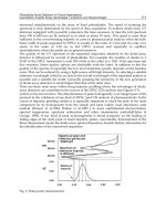
To inspect the relationship between diffusion depth and diffusion time, the electrochemical
C-V (ECV) measurement was applied. The diffusion-depth test was applied to a 3 μm thick
undoped InP epitaxial layer which was grown on an n
+
-InP substrate. The diffusion process
was performed at 550ºC in a RTA with N
2
-purged ambient, and the rising ramp rate of
temperature was set to 5ºC/sec. After driving in of Zn diffusion source and removing
residual glass and dielectric, the diffused wafer routinely underwent RTA process for
impurity activation while virtually eliminating the potentially damaged interstitial zinc. Fig.
2 shows the concentration profiles for the various thermal treatment condition (ramping
rate/temperature/time). The thermal treatment condition used for PD fabrication is 600ºC
RTA for 25 sec in N
2
ambient. This shows that most Zn atoms are activated and act as
acceptors. The net-acceptor concentrations are around 2-4 x 10
18
cm
-3
in all of the samples.
Similar SOD technology is also applied to the case of GaSb wafer. The fabricated p-n
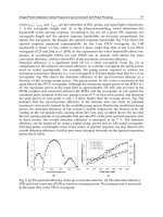
junction structure is shown in the inset of Fig. 3. The diffusion depth measured by
electrochemical C-V profiler is shown in Fig. 3. The junction depth is 0.6 μm and the
concentration of surface can be achieved as high as around 5 × 10
20
cm
-3
.
Photodiodes with High Speed and Enhanced Wide Spectral Range
7
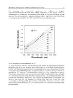
Fig. 2. Concentration profiles of spin-on Zn diffusion in undoped InP after 600ºC RTA for 25
sec in N
2
ambient
Fig. 3. The diffusion depth measured by electrochemical C-V profiler. The inset of Fig. 3
shows the fabricated p-n junction structure.
Photodiodes – Communications, Bio-Sensings, Measurements and High-Energy Physics
8
3. Fabrication of InGaAs/InP p-i-n photodiodes [10]
The InP/InGaAs/InP p-i-n PD is constructed to be capable of speedily and efficiently
detecting light signals of wavelengths ranging from 0.7 m to 1.65 m. This range covers all
the wavelengths of interest nowadays in fiberoptic communications: 0.85 m, 1.3 m, and
1.55 m.
The InP/InGaAs/InP epitaxial device structure was grown by metal-organic chemical vapor
deposition (MOCVD) on the n
+
-InP substrate. A first layer of 0.5-m undoped InP was
grown for buffering the growth process. A second layer of 2.5-m undoped indium gallium
arsenide (InGaAs) was grown for light absorption layer. A third layer of 1.0-m undoped
InP was grown as the wide-bandgap cap layer. Highly reliable SAD planar device process,
either by sealed-ampoule diffusion or spin-on diffusion, was utilized for device fabrication.
Silicon nitride (SiN
x
) film with 1500-Å thickness was deposited onto the entire wafer by
plasma-enhanced chemical vapor deposition (PECVD). Through conventional
photolithographic process and reactive ion etching (RIE), diffusion windows with 50-m
diameter were opened on the dielectric film. Afterwards, wafer was loaded into semi-closed
diffusion system and zinc (Zn)–diffusion process was performed at 550℃ for 10 min. Such a
temperature and period produced a 10
17
cm
-3
acceptor front at 1.2-m deep below the
surface. Due to a rather slow diffusion of Zn in InGaAs (3 times slower than that in InP), the
Zn protrusion depth into the InGaAs can be well controlled to be about 0.1-0.2 m, which
was designed for reliability, wide spectral range, and high-speed operation considerations.
After impurity activation by RTA and conventionally photolithographic process, ring-
shaped p-contact metallization chromium (Cr)/gold (Au)/AuZn/Cr was deposited on
heavily doped p-type InP cap layer. The contact adhesion was enhanced by heat treatment.
Then the InP cap layer inside the 30-m-diameter coupling aperture was removed by a
reactive ion etching with the CH
4
/H
2
source to slightly etch and recondition the InP surface
and then by chemical etching based on the 3H
3
PO
4
: HCl solution to selectively clean the InP
thickness left. Afterwards, double-layer SiN
x
/SiO
x
antireflection (AR) coating and Cr/Au
for bondpad metallizations were deposited in sequence. Wafers were then lapped and
polished down to about 150 m and the polished backside was coated with Ti/Pt/Au n-
contact metallizations. Lastly, samples were annealed at 420℃ for 20 sec to reduce the
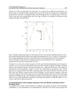
contact resistance. The cross-sectional view of a finished device is schematically drawn in Fig.
4. Then the wafer was separated into chips, and several were packaged for characterizations.
The essence of this PD is to remove the InP cap layer inside the illumination aperture
(directly above the light-absorption layer) while leave a shallow p-n junction in the narrow-
bandgap InGaAs absorption layer. Also, the contact is made on the thick-enough InP cap
layer for preventing the alloy spike from shortening device layers with opposite conducting
types. There are several critical considerations in performing this art.
First, a well-controlled diffusion process needs to be established. The junction protrusion
depth into the InGaAs absorption layer is consequential. Too shallow junction depth would
result in the following two detrimental effects: surface depletion and large sheet resistance.
The former leads to large dark leakage even at low bias, while the latter results in non-
uniform spatial response. To the other extreme, deep junction results in excessive absorption
in the quasi-neutral p-type region. Electrons generated in this low-field region slowly
diffuse (as compared to drift process) out of the region or recombine with holes. As a
consequence, low-efficiency and low-speed device performance can be expected for certain
Photodiodes with High Speed and Enhanced Wide Spectral Range
9
Fig. 4. Schematic drawing of device cross section. Note the absence of the InP cap inside the
aperture.
wavelength operation. Shorter wavelength typically has a larger absorption coefficient that
is equivalent to a shallower absorption depth, and vice versa. How deep the junction can
protrude into the InGaAs absorption layer is thus quite dependent on the operating
wavelength for avoiding slow carrier diffusion process. Typically the depth is designed
about the reciprocal of the absorption coefficient corresponding to the minimum
wavelength the detector operates.
Second, a well-controlled etching process is required to remove the InP cap layer inside the
aperture region. Due to the target region is surrounded by contact metallizations, the metal
films should adhere to the cap layer well enough for inhibiting non-uniform and excessive
localized undercut during wet etching process. The wet etching time should also be
controlled. Excessive undercut could expose the junction periphery in the InGaAs
absorption layer and consequently result in severe surface leakage, which could go further if
there would be process-induced damages. It would be advantageous to have the
metal/semiconductor interface slightly alloyed before etching process. By using a wider p-
contact span “s” or adopting a second dielectric passivation, the wet etching process can be
more tolerable. Of course, this benefit is at the price of reduced coupling aperture. Besides
adhesion consideration, dry etching process can be performed as an assist before wet
process to minimize undercut. Nevertheless, to avoid impact damages, some thickness of
cap layer should be left for wet process. It is essential that the wet process has desired
selectivity; that is, the etching process stops automatically once the etching solution sees the
absorption layer. If the etching solution or the material system has poor selectivity, the
etching time should be accurately controlled, otherwise the shallow p-n junction can be also
removed and, as a consequence, no biasing field for generated carriers.
Photodiodes – Communications, Bio-Sensings, Measurements and High-Energy Physics
10
Third, for high efficiency in all the operating spectral range, device has an anti-reflection
dielectric coating designed for the wavelengths of interest. It is impossible for single-layer
dielectric film to serve a broad spectral range. Therefore, at least two layers of dielectric
films are required.
4. Device characteristics [10]
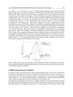
Fig. 5 shows both current-voltage (I-V) and capacitance-voltage (C-V) characteristics of the
devices measured at room temperature. Typically, the InGaAs PD exhibits a 50-pA dark
current and a 0.3-pF capacitance at –5 V. Obviously from this figure, the device leakage
behaves just as of those conventional planar InGaAs p-i-n PDs, which keeps a slightly
increasing leakage as the bias increases till the tunneling-type breakdown is reached. Such a
low dark current indicates that the InP cap is removed without generating the surface
damage and the severe undercut, which might expose the junction periphery in InGaAs. In
addition, the sheet resistance of the p
+
-InGaAs layer was measured as about 720 Ω/,
which is comparable to that of the p
+
-InGaAs base of the InP-based heterojunction bipolar
transistors (HBTs) [15]. The measured series resistance of the InGaAs PD is about 18 Ω,
which indicates that the 0.1-0.2 m p
+
-InGaAs layer has been doped high enough (~10
19
cm
-
3
) for high-speed applications. The low capacitance indicates a well-controlled junction
depth and a significantly reduced parasites, which results in a 0.1-pF junction capacitance
and a 0.2-pF parasitic capacitance, respectively. The estimated frequency response deduced
from the series resistance and the measured capacitance is about 10.1 GHz.
Fig. 5. Characteristics of dark current and capacitance versus reverse bias at room
temperature.