Photodiodes Communications Bio Sensings Measurements and High Energy Part 3 pptx
Bạn đang xem bản rút gọn của tài liệu. Xem và tải ngay bản đầy đủ của tài liệu tại đây (3 MB, 20 trang )
Evaluation of Uni-Traveling Carrier Photodiode
Performance at Low Temperatures and Applications to Superconducting Electronics
31
of the customized modules. On the other hand, misalignment did not occur for the standard
one. The cause of the misalignment was due to the bending of the optical fiber. The problem
was finally resolved by shortening the free space of the fiber without ferrule and by
uniformly gluing the fiber to the ferrule with epoxy resin, as shown in Fig. 5(a). Figure 5(b)
is a photograph of the entire module, which has a coaxial V-connector for a wide-band
electrical output and DC terminals.
(a) (b)
Fig. 5. Photographs of customized UTC-PD; (a) UTC-PD chip and fiber lens and (b) entire
module.
The equivalent circuit of a negative type UTC-PD module is shown in Fig. 6. In the negative
type, the UTC-PD module is usually negatively biased to accelerate electron drift in the
depletion layer, increasing the operating speed. The output signal is inverted to the input
signal. A termination resistor of 50 for impedance matching is integrated at the output of
the chip.
Fig. 6. Equivalent circuit of negative-type UTC-PD module.
2.3 DC characteristics at low temperature
The current versus voltage (I-V) characteristics of our customized UTC-PD module was
measured at operating temperatures from 4 to 300 K, as shown in Fig. 7. No electrical and
Photodiode chip
200 pF2200 pF
50
V
bias
(negative)
50
Output
Photodiode chip
200 pF2200 pF
50
V
bias
(negative)
50
Output
Photodiodes – Communications, Bio-Sensings, Measurements and High-Energy Physics
32
mechanical damage was observed from the I-V characteristics in our experiments when the
UTC-PD module was cooled using a cryocooler at a cooling rate of around 1 degree/minute.
Since the gap energy of the InGaAs increased and thermal energy decreased, the forward
voltage, at which the current rapidly increased, somewhat increased. The forward voltage
increased around 0.16 V by cooling from 300 K to 4 K. The forward current increased
sharply at this forward voltage as the operating temperature decreased.
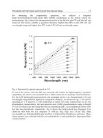
Dependence of optical sensitivity on temperature was measured for both modules, as shown
in Fig. 8. The optical wave length was 1550 nm and the input optical power was 0.7 W. Both
the UTC-PD modules were biased at -2 V, and the output voltage was measured with a digital
voltmeter. The output voltage decreased as the temperature decreased. The output voltage of
the standard UTC-PD module was larger than that of customized UTC-PD module over the
entire temperature range. The temperature dependences, however, showed relatively similar
changes between the two modules. The difference in the results for the two modules was
probably due to the difference in the coupling efficiency between the lens and the chip. The
output voltage of the customized module is still large enough. We can, therefore, conclude that
the customized module using a fiber lens is useful for most applications that require a non-
magnetic environment, such as those for superconducting devices.
Fig. 7. Current versus voltage (I-V) curves at temperatures between 6 and 294 K.
3. High-frequency and high-speed operation
The high-frequency response of a UTC-PD module at low temperature is important. We
evaluated this response using a high-speed optical measurement system. We needed several
electronic and optical instruments to produce an optical signal modulated with various high-
speed bit pattern signals. The measurement system and the high-speed response of our
customized UTC-PD module are discussed in this section. The cryocooling system for cooling
the customized UTC-PD module and superconducting devices is discussed in the next section.
0 0.2 0.4 0.6 0.8
0
0.2
0.4
0.6
294 K
233 K
160 K
120 K
6 K
Voltage (V)
Current (mA)
Evaluation of Uni-Traveling Carrier Photodiode
Performance at Low Temperatures and Applications to Superconducting Electronics
33
Fig. 8. Temperature dependence of sensitivity of standard and customized UTC-PD modules.
3.1 Optical input measurement system
Figure 9 shows a block diagram of the optical measurement system, which can output 47-
Gbps high-speed optical signals. The main clock signal is generated with a signal generator
(Anritsu MG3695B: 2 - 50 GHz), and the pulse pattern is generated with a 4-channel pulse
pattern generator (Anritsu MP1758A: 10 MHz - 12.5GHz) and serialized with a multiplexer
(MUX), which enables us to generate a non-return-to-zero (NRZ) pulse pattern of up to 47
GHz. The MUX and pulse pattern generator (PPG) were synchronized and the timing of the
digital data from the PPG to the clock signal in the MUX was adjusted with delay lines. An
electrical/optical (E/O) converter with a MUX (Anritsu MP1806A), which includes a laser
diode, an optical modulator with an automatic bias controller (ABC), generated arbitrary
optical digital pattern signals with a modulation depth of almost 100%. The optical signal
was amplified with an erbium-doped fiber amplifier (EDFA) and the output power was
adjusted with a power controller and attenuator (Agilent 8163B). The controlled output
signal was applied to the customized UTC-PD module, which converted the optical signal to
an electrical signal at around 4 K. The electrical output was connected to a cryoprobe, which
was also cooled at around 4 K, through a 1.19-mmcopper coaxial cable of 230 mm in
length.
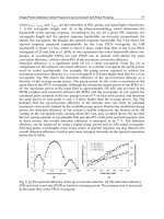
3.2 High-frequency performance
The high-speed performance of the customized UTC-PD module cooled around 4 K was
measured and confirmed for up to a 40-Gbps NRZ signal. The customized UTC-PD module
was set on the 2
nd
stage in the cryocooling system, which is discussed in Section 4.1. Figures
10(a) and (b) show typical eye diagrams of the input optical signal and the output electrical
signal observed with a sampling oscilloscope (Agilent 86100C). The modulation depth was
automatically adjusted to almost 100%. The input signal was a pseudo random bit stream
(PRBS) signal with a data length of 2
31
-1. A block diagram of the measurement system is
0 100 200 300
0.2
0.4
0.6
0.8
Temperature (K)
Sensitivity of UTC-PD (A/W)
Standard (Upper)
Customized (Lower)
0 100 200 300
0.2
0.4
0.6
0.8
Temperature (K)
Sensitivity of UTC-PD (A/W)
Standard (Upper)
Customized (Lower)
Photodiodes – Communications, Bio-Sensings, Measurements and High-Energy Physics
34
shown in Fig. 9. The output line includes a loss of 2.8 dB at 40 GHz in a 510-mm-long coaxial
cable in the cooling system.
Fig. 9. Setup of optical measurement system that can produce optical digital signal at data
rate of up to 47 Gbps
The amplitude of the output signal was 90 mV in a peak-to-peak voltage for an input optical
signal power of 10 mW at a wavelength of 1550 nm. We evaluated the linearity for the
amplitude of the output voltage to the optical input signal power. Since there was no
difference observed for the data length between 2
31
-1 and 2
7
-1 of the PRBS signals, a data
length of 2
7
-1 was used to save time. Figure 11 shows the optical input power versus the
output voltage for 10, 20, and 40-Gbps PRBS data input, resulting in good linearity over the
input optical power of 10 mW. In the above evaluation, the customized UTC-PD module
(a) (b)
Fig. 10. Eye patterns of (a) optical output signal of optical measurement system for 31-stage
pseudo random bit stream (PRBS) digital signal and (b) electrical output signal of
customized UTC-PD module cooled at 5 K.
GND
level
90 mV
GND
level
90 mV
GND
level
90 mV
GND
level
90 mV
UTC-PD
module
Attenuator
EDFALaser
Modulator
MUX with E/O
Voltage
Pulse at f
clk
ABC
Multiplexer (MUX)
PPG (4ch)
4-channel
data
f
clk
/4
f
clk
Signal
generator
4 -10K
Superconductive
microchip
Optical
Pulse at f
clk
Cryocooling system
UTC-PD
module
Attenuator
EDFALaser
Modulator
MUX with E/O
Voltage
Pulse at f
clk
ABC
Multiplexer (MUX)
PPG (4ch)
4-channel
data
f
clk
/4
f
clk
Signal
generator
4 -10K
Superconductive
microchip
Optical
Pulse at f
clk
Cryocooling system
Evaluation of Uni-Traveling Carrier Photodiode
Performance at Low Temperatures and Applications to Superconducting Electronics
35
was DC biased at -2 V, which is definitely required for high-speed performance at room
temperature. It should be noted that the customized UTC-PD module operated at high
speed even at zero DC bias voltage, which may be due to the increment of the built-in
electric field in the absorption and depletion layers.
Fig. 11. Electrical output voltages as function of optical input power of customized UTC-PD
module cooled at 5 K for 10, 20, and 40-Gbps PRBS data input.
4. Applications of UTC-PD module operating at cryogenic temperature to
superconducting electronics
The optical link of the input signal between semiconducting devices operating at room
temperature and superconducting devices at cryogenic temperature has several advantages.
The thermal conductivity of optical fibers is extreamly small compared with metal-based
electric links, such as coaxial and flexible film cables. The themal conductivity of quatz,
which is a base material in a single-mode opitical fiber, is 1.4 W/m/K; therefore, the thermal
conductivity of a single-mode optical fiber having a crad diameter of 125 m and a length of
1 m is as small as 5.2 x 10
-6
W. The signal loss is also extremely small, e.g., < 0.2 dB/km for a
wavelength of 1550 nm and < 0.4 dB/km for 1310 nm. The signal loss of the optical fiber is
negligible for our applications such as analogue to digital converters (ADC) using SFQ
circuits, which require short distance transmission. It is small enough even if we use a
longer, e.g., 1 km, optical fiber. The signal loss seems to be rather large at optical connectors
and other parts.
4.1 Cryocooling system for superconducting electronics system
Single flux quantum circuits have been investigated for superconducting digital and
analog/digital applications. In most of these investigations, superconducting IC chips were
cooled by directly immersing them in liquid helium. It is convenient to cool IC chips to
cryogenic temperature for laboratory use due to the immediate cooling time. Many
Input: PRBS7
0
10
20
30
40
50
60
70
024681012
Optical Input (mW)
Electrical output (mV
p-p
)
10 Gbps
20 Gbps
40 Gbps
Input: PRBS7
0
10
20
30
40
50
60
70
024681012
Optical Input (mW)
Electrical output (mV
p-p
)
10 Gbps
20 Gbps
40 Gbps
10 Gbps
20 Gbps
40 Gbps
Photodiodes – Communications, Bio-Sensings, Measurements and High-Energy Physics
36
superconducting systems, however, require a cryocooler for practical applications. Even for
laboratory use, a cooling system using a cryocooler is desirable for system-level tests and
high-speed or high-frequency tests because the signal loss and distortion between room
temperature and cryogenic temperature may especially cause problems and restrict
experiments. A cryocooling system using a two-stage 4-K Gifford MacMahon (GM)
cryocooler was developed at the international Superconductivity Technology Center
(ISTEC) for demonstrating superconducting digital and analog ICs based on the
Nb/AlOx/Nb Josephson junctions. A photograph and illustration of the system is shown in
Fig. 12. The 2
nd
cold stage, 4-K stage, including a superconducting chip, a cryoprobe, and
our customized UTC-PD module is surrounded with a thermal shield with a temperature of
50 K using the 1
st
cold stage of the cooler. Cryogenic amplifiers are attached to the thermal
shied. The cryocooler (RDK-408D) and the compressor (CSA-71A) are from Sumitomo
heavy industries Ltd. The cooling capacity is 1 W at 4.2 K for the 2
nd
cold stage and 60 W at
50 K for the 1
st
cold stage. The total input AC power of the cooler is 6.5 kW. The system has
twenty-four high-frequency I/O terminals with V-connectors and two optical input ports
using the customized UTC-PD module. The 1
st
cold stage of the cooler, the 50-K stage, can
effectively be used for cooling the cryogenic amplifiers, thermal shied, and thermal anchor.
Fig. 12. Cryocooling system for supeconducting devices. Left is photograph of system and
right is cross-sectional illustration.
Figure 13 shows a photograph of the 2
nd
stage arrangement with a cryoprobe and two
customized UTC-PD modules placed on the sub 2
nd
cold stage located in a short distance
around 100 mm from the SFQ multi-chip module (MCM) on the main 2
nd
stage, as shown in
Figs. 12 and 13; therefore, the temperature was a little high, between 5-6 K. We developed
MCM technology with flip-chip bonding and a cryoprobe for superconducting systems,
which enable us to conduct high-speed measurements of superconducting circuits. The SFQ
Electrical I/O port
Vacuum chamber
(H30 × W36 × L48 cm)
Cryogenic
amplifier
2-stage GM cryocooler
Cryoprobe head
2
nd
main stage
(~4 K)
1
st
stage
(~50 K)
2
nd
sub stage
(~4 K)
50-K shield
Magnetic shield
SFQ MCM
Optical I/O port
UTC-PD
Optical
fiber
Co-axial
cable
Thermal link
(Silver)
Electrical I/O port
Vacuum chamber
(H30 × W36 × L48 cm)
Cryogenic
amplifier
2-stage GM cryocooler
Cryoprobe head
2
nd
main stage
(~4 K)
1
st
stage
(~50 K)
2
nd
sub stage
(~4 K)
50-K shield
Magnetic shield
SFQ MCM
Optical I/O port
UTC-PD
Optical
fiber
Co-axial
cable
Thermal link
(Silver)
Evaluation of Uni-Traveling Carrier Photodiode
Performance at Low Temperatures and Applications to Superconducting Electronics
37
chips mounted on the MCM substrate including the cryoprobe was attached to the main 2
nd
stage, which was magnetically shielded with a two-folded permalloy enclosure. However,
the customized UTC-PD module was placed outside the magnetic shield. The main 4-K
stage was cooled with thermal conduction through a thermal link made of silver and the
magnetic shield from the 2
nd
cold head of the cryocooler. The vibration of the temperature at
the main 4-K stage was then stabilized to as low as 10 mK, which ensured the stable
operation of SFQ circuits.
Fig. 13. Arrangement of 4-K cold stages in cooling system; superconducting IC chip with
multi-chip module (MCM) and cryoprobe surrounded by double magnetic shield (right
side; the lids are removed to show the contents) on main cold stage, and customized UTC-
PD module operating at 4 K for introducing high-frequency optical signal into cryostat
through optical fiber was placed on sub-cold stage.
4.2 Superconducting single flux quantum (SFQ) digital circuits
We designed an SFQ circuit chip, which includes an input interface between the customized
UTC-PD module and SFQ circuit. Figures 14 (a) and (b) show an equivalent circuit and a
microphotograph of the PD/SFQ converter. The chip was fabricated with the ISTEC
standard process 3 (STP3) using Nb/AlOx/Nb Josephson junctions with a current density of
10 kA/cm
2
. The input signal was magnetically coupled to the SFQ circuit, making it possible
to accept both polarities of the input signal by changing the direction of the coupling in the
transformer. The negative polarity signal from the customized UTC-PD module was then
able to be received directly without any offset current and inverter by the PD/SFQ converter
shown in Fig. 14. Josephson junctions, J1 and J2, and inductances, L1 and L2, construct a
superconducting quantum interference device (SQUID). When the input signal, data “1”, is
applied, the SQUID stores the single flux quantum in the superconducting loop, producing
clockwise circulating current. By applying the clock pulse, the SFQ pulse is output by
switching J2 and J3. When data “0” is applied, no SFQ pulse is output. In this case, the SFQ
4-K sub-stage
UTC-PD module
Electrical output of UTC-PD
Optical fiber
MSL
Cryoprobe
Superconducting
device MCM
Magnetic shield
(lower half)
4-K main-stage
4-K sub-stage
UTC-PD module
Electrical output of UTC-PD
Optical fiber
MSL
Cryoprobe
Superconducting
device MCM
Magnetic shield
(lower half)
4-K main-stage
Photodiodes – Communications, Bio-Sensings, Measurements and High-Energy Physics
38
pulse produced by the clock pulse is escaped from J5. The converter can then produce SFQ
pulses from the normal NRZ signal from the customized UTC-PD module, where the SFQ
pulse
15
0
() /2 ~2.07 10 [ ]Vtdt h e Wb
(1)
acts as the quantized information medium in SFQ circuits.
(a) (b)
Fig. 14. UTC-PD to single flux quantum (SFQ) converter; (a) equivalent circuit and (b)
microphotograph.
The SFQ circuit chip for testing the optical input link is composed of the PD/SFQ convertor,
a 1-2 demultiplexer (DEMUX), and two NRZ superconducting voltage drivers (SVDs), as
shown in Fig. 15. Signal flux quantum pulses have a narrow width (~2 ps) and a low signal
level (~1 mV), and the circuit can be operated faster than that in semiconductor devices. The
SFQ output data of the PD/SFQ is alternately output to the two outputs with the 1:2
DEMUX in parallel to reduce the output data rate to half the input data rate. Then, the SFQ
pulse signal is converted to an NRZ signal by the SVDs.
Figure 16 shows an NRZ SQUID voltage driver (NRZ SVD). This NRZ SVD consists of a
splitter (SPL), which divides a single SFQ signal into 16 splitter outputs, RS flip-flops
(RSFFs), each of which stores an SFQ signal, and 16 serially connected SQUIDs, which
amplify the SFQ signal stored in the RSFF to 2-mV NRZ data streams up to 23.5 GHz. There
are a total of 318 junctions, and the bias current is 43 mA. The 5 x 5 mm SFQ chip was flip-
chip bonded on a 16 mm x 16 mm MCM carrier with InSn bumps, as shown in Fig. 17(a).
Both the chip and carrier are made of the same Si substrate, which prevents stress due to
the difference in thermal expansion coefficients when they are cooled. Figure 17 (b) shows
InSn bumps for the signal and ground, in which the signal bump was connected to a 50
micro-strip line (MSL) in the chip. The height of the bump was as small as 8 m, as shown
in Fig. 17(c), which enabled us to transmit high-frequency signals over 100 GHz. The
MCM carrier was mounted on the 4-K main base plate of the cryoprobe, as shown in Fig.
13. Copper-molybdenum alloy was chosen as the base plate material to decrease the
difference in the thermal expansion coefficient. The cryoprobe was adjusted to ensure
contact of the chip pads. The optical link was tested using the test circuit at a high-speed
data rate.
bias
DC
dat_in
clk_in
out
J1 J2
65m
bias
bias
DC
dat_in
clk_in
out
J1 J2
65m
bias
bias clk_in
out
DC
dat_in
J1 J2 J3
J4
J5
L1 L2
LD1 LD2
LIN1 LIN2 R
term
R
term
biasbias clk_in
out
DC
dat_in
J1 J2 J3
J4
J5
L1 L2
LD1 LD2
LIN1 LIN2 R
term
R
term
bias
bias
DC
dat_in
clk_in
out
J1 J2
65m
bias
bias
DC
dat_in
clk_in
out
J1 J2
65m
bias
bias clk_in
out
DC
dat_in
J1 J2 J3
J4
J5
L1 L2
LD1 LD2
LIN1 LIN2 R
term
R
term
biasbias clk_in
out
DC
dat_in
J1 J2 J3
J4
J5
L1 L2
LD1 LD2
LIN1 LIN2 R
term
R
term
bias
Evaluation of Uni-Traveling Carrier Photodiode
Performance at Low Temperatures and Applications to Superconducting Electronics
39
PD/SFQ
1:2
DEMUX
NRZ DRV
NRZ DRV
clk_in
dat_in
DC
out1
out2
f/1 data
f/1 clock
f/2 data
f/2 clock
PD/SFQ
1:2
DEMUX
NRZ DRV
NRZ DRV
clk_in
dat_in
DC
out1
out2
f/1 data
f/1 clock
f/1 data
f/1 clock
f/2 data
f/2 clock
1:2
DEMUX
NRZ DRV
PD/SFQ
NRZ DRV
1:2
DEMUX
NRZ DRV
PD/SFQ
NRZ DRV
Fig. 15. Block diagram and microphotograph of SFQ test chip for optical input.
Photodiodes – Communications, Bio-Sensings, Measurements and High-Energy Physics
40
(a) (b)
Fig. 16. Non-return-to-zero (NRZ) superconducting quantum interference device (SQUID)
voltage driver; (a) block diagram and (b) microphotograph.
(a)
(b) (c)
Fig. 17. Photographs of, (a) flip-chip bonded MCM carrier and superconducting micro-chip,
(b) flip-chip bumps on chip, and (c) cross sectional view of flip-chip bonded bump.
SPL
(1→16)
RSFF
M
RSFF
SQ
SQ
SQRSFF
reset
set
SQUID bias
out
16 stage
SPL
(1→16)
RSFF
M
RSFF
SQ
SQ
SQRSFF
reset
set
SQUID bias
out
16 stage
reset
set
400 mm
520 mm
RSFF+SQUIDSPL
reset
set
400 mm
520 mm
RSFF+SQUIDSPL
SPL
(1→16)
RSFF
M
RSFF
SQ
SQ
SQRSFF
reset
set
SQUID bias
out
16 stage
SPL
(1→16)
RSFF
M
RSFF
SQ
SQ
SQRSFF
reset
set
SQUID bias
out
16 stage
reset
set
400 mm
520 mm
RSFF+SQUIDSPL
reset
set
400 mm
520 mm
RSFF+SQUIDSPL
Evaluation of Uni-Traveling Carrier Photodiode
Performance at Low Temperatures and Applications to Superconducting Electronics
41
The output signals of the SVDs are further amplified by GaAs cryogenic amplifiers mounted
on the 1
st
stage of the cryocooling system, as shown in Fig. 12. The cryogenic amplifier,
SHF105C, was developed by SHF communication Technology AG originally for SFQ circuits
in collaboration with ISTEC. The output voltage of the SVDs was amplified to around 50 mV
with the cryogenic amplifiers, which have a gain of around 30 dB at 23 K and a typical
bandwidth of 30 GHz. The optical digital data of up to 47 Gbps was applied to the
customized UTC-PD module, and the converted electrical signal was applied to the test chip
through a Cu coaxial flexible cable of 1.19 mm in diameter and length of 230 mm. Figure 18
shows the experimental results for the input data rate of 47-Gbps data; (a) the outputs of the
two SVDs for patterned digital data and (b) eye pattern for PRBS of 2
31
-1. We can clearly see
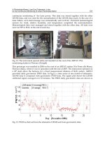
an open eye pattern. The bit error rate (BER) was measured with an error detector
(Advantest D3286). Figure 19 shows the dependences of the BER for PRBS of 2
7
-1, (a) on the
bias current of the PD/SFQ converter and (b) on the input optical power. Sufficiently small
BER of less than 10
-12
at 40 Gbit/s in the output was obtained with the test circuit for the
optical input signal through the customized UTC-PD module as an O/E converter.
Fig. 18. Experimental results of optical input at data rate of 47 Gbps using SFQ test chip; (a)
23.5-Gbps digital output waveforms of two SQUID drivers and (b) eye pattern of one output
for PRBS data input.
out1 (23.5-Gbps NRZ)
out2 (23.5-Gbps NRZ)
0011011100100110
0000101001011111
100 ps
out1 (23.5-Gbps NRZ)
out2 (23.5-Gbps NRZ)
0011011100100110
0000101001011111
100 ps
out1 (23.5-Gbps NRZ)
out2 (23.5-Gbps NRZ)
0011011100100110
0000101001011111
100 ps
out1 (23.5-Gbps NRZ)
out2 (23.5-Gbps NRZ)
0011011100100110
0000101001011111
100 ps
(a)
(b)
Photodiodes – Communications, Bio-Sensings, Measurements and High-Energy Physics
42
Fig. 19. Bit error rate (BER) as function of (a) bias current of PD-SFQ converter and (b)
optical input power for UTC-PD module.
4.3 Josephson voltage standards
Josephson voltage standards (JVS) have been used as a DC voltage standard since 1990
because of their quantum mechanical accuracy. These standards consist of an under-
damped superconductor-insulator-superconductor (SIS) junction array, which is DC biased
and radiated with microwave. The voltage is determined with the microwave frequency and
physical constant, which ensure its quantum mechanical accuracy. Although, JVS are
suitable for DC voltage standards, they cannot be applicable to AC voltage standards.
Because JVS use the hysteresis of SIS junctions, a proper procedure for applying the DC bias
and microwaves and time to fix to the desired voltage is required.
The pulse-driven Josephson arbitrary waveform synthesizer (PD-JVS) is a device for
producing AC voltage standard, which is one of AC JVS. This device is also called as
Josephson arbitrary waveform synthesizer (JAWS). The principle is based on a 1-bit sigma
delta digital-to-analog converter. The basic idea is that the amplitude of a signal waveform
is represented as a pulse density. The pulse pattern is properly calculated for desired
waveform and generated with a pulse pattern generator, which is applied to a JAWS chip.
The JAWS chip consists of over-damped Josephson junction arrays (JJAs), which are capable
of producing quantized voltage pulses. High-speed pulses, of which a pattern is calculated
for producing the desired waveform, is generated in room-temperature electronics, and the
optical signal is transferred to an electrical signal with the customized UTC-PD module at
cryogenic temperature, which enables us to apply the high-speed signal to the SFQ chip
with extremely low noise as well as low signal losses and distortions. The operation of the
synthesizer was demonstrated by the National Institute of Advanced Industrial Science and
Technology (AIST) and ISTEC using the cooling system with the customized UTC-PD
module. We have to use junctions without hysteresis for the JAWS. The JAWS chips were
fabricated in two superconducting microchip processes; one with Nb/AlOx/Al/AlOx/Nb
Josephson junctions, which are superconductor-insulator-normal metal-superconductor
(SINS) junctions, developed by ISTEC, and the other with NbN/TiNx/NbN junctions,
which are superconductor-normal metal-superconductor (SNS) junctions, developed by
AIST. Figure 20 shows an IC chip fabricated with the Nb/AlOx/Al/AlOx/Nb junctions.
The chip consists of an array of 100 serially connected junctions, which can increase the
output voltage. The array was arranged in the center of a 50 coplanar waveguide input
line in the chip. The 5 x 5 mm chip was flip-chip bonded on the MCM carrier, in the same
manner as SFQ chips. PD-JVS chips were also fabricated with the NbN/TiNx/NbN
7.5 X 10
-14
1.E -14
1.E -13
1.E -12
1.E -11
1.E -10
1.E -09
1.E -08
1.E -07
1.E -06
1.E -05
1.E -04
1.E -03
1.E -02
1.E -01
1.E +00
0.18 0.2 0.22 0.24 0.26 0.28 0.3 0.32 0.34
PD/SF Q bias [mA]
BER
7.5 X 10
-14
1.E -14
1.E -13
1.E -12
1.E -11
1.E -10
1.E -09
1.E -08
1.E -07
1.E -06
1.E -05
1.E -04
1.E -03
1.E -02
1.E -01
1.E +00
0.18 0.2 0.22 0.24 0.26 0.28 0.3 0.32 0.34
PD/SF Q bias [mA]
BER
3.8 X 10
-14
1.E-14
1.E-13
1.E-12
1.E-11
1.E-10
1.E-09
1.E-08
1.E-07
1.E-06
1.E-05
1.E-04
1.E-03
1.E-02
1.E-01
1.E+ 00
12345678
Optical input power [mW]
BER
3.8 X 10
-14
1.E-14
1.E-13
1.E-12
1.E-11
1.E-10
1.E-09
1.E-08
1.E-07
1.E-06
1.E-05
1.E-04
1.E-03
1.E-02
1.E-01
1.E+ 00
12345678
Optical input power [mW]
BER
7.5 X 10
-14
1.E -14
1.E -13
1.E -12
1.E -11
1.E -10
1.E -09
1.E -08
1.E -07
1.E -06
1.E -05
1.E -04
1.E -03
1.E -02
1.E -01
1.E +00
0.18 0.2 0.22 0.24 0.26 0.28 0.3 0.32 0.34
PD/SF Q bias [mA]
BER
7.5 X 10
-14
1.E -14
1.E -13
1.E -12
1.E -11
1.E -10
1.E -09
1.E -08
1.E -07
1.E -06
1.E -05
1.E -04
1.E -03
1.E -02
1.E -01
1.E +00
0.18 0.2 0.22 0.24 0.26 0.28 0.3 0.32 0.34
PD/SF Q bias [mA]
BER
3.8 X 10
-14
1.E-14
1.E-13
1.E-12
1.E-11
1.E-10
1.E-09
1.E-08
1.E-07
1.E-06
1.E-05
1.E-04
1.E-03
1.E-02
1.E-01
1.E+ 00
12345678
Optical input power [mW]
BER
3.8 X 10
-14
1.E-14
1.E-13
1.E-12
1.E-11
1.E-10
1.E-09
1.E-08
1.E-07
1.E-06
1.E-05
1.E-04
1.E-03
1.E-02
1.E-01
1.E+ 00
12345678
Optical input power [mW]
BER
Evaluation of Uni-Traveling Carrier Photodiode
Performance at Low Temperatures and Applications to Superconducting Electronics
43
junctions, in which 480 junctions were serially connected to increase the output voltage. The
chip using the NbN junctions can operate at higher temperatures than that using the Nb
junctions, which enable us to use a 10-K cryocooler.
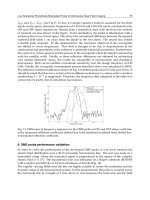
Fig. 20. Microphotograph of pulse-driven Josephson arbitrary waveform synthesizer (PD-
JVS) chip fabricated with Nb/AlOx/Al/AlOx/Nb junction technology.
The JAWS can produce any waveform by applying a properly calculated pulse pattern. Figure
21 shows examples of synthesized waveforms; (a) triangular, (b) rectangular, and (c) saw-
tooth. The left charts show the frequency spectrum and the right ones show generated
waveforms. A high-precision sine wave was generated with a JAWS chips fabricated with both
Nb/AlOx/Al/AlOx/Nb and NbN/TiNx/NbN Josephson junctions. Figure 22 shows the
frequency spectrum of a 152.6-kHz sine wave with the PD-JVS using the Nb junctions. The
sampling frequency was 10 GHz and the output voltage of 1.24 mV with spurious free
dynamic range (SFDR) of -75 dBc was obtained from the chip. Figure 23 shows the frequency
spectrum of a 59.6-Hz sine wave generated with the 480 NbN-SNS junctions, of which the
frequency is important because it is around the commercial (mains) frequencies of 50 and 60
Hz. The sampling frequency was 8 GHz and a 134,217,728-bit-long (=2
27
bit) binary pulse
pattern was used for generating the 59.6-Hz sine wave. A sine wave was clearly observed with
both PD-JVS chips. However, the SFDR was limited to -67 dBc due to odd harmonics of 50 Hz.
The SFDR omitting these harmonics was as low as -80 dBc. The reduction of signal-to-noise
Photodiodes – Communications, Bio-Sensings, Measurements and High-Energy Physics
44
ratio (SNR) due to the odd harmonics of 50 Hz seemed to be affected by noise from the ground
loops. The ground noise could be avoided by isolating the grounds in the I/Os.
Fig. 21. Examples of frequency spectrum and waveforms synthesized using PD-JVS; (a)
triangular, (b) rectangular, and (c) saw-tooth.
Fig. 22. Frequency spectrum of synthesized sine wave of 152.6 KHz with the PD-JVS using
Nb/AlOx/Al/AlOx/Nb junctions.
-80
-60
-40
-20
0
FFT amplitude (dB)
1.00.80.60.40.20.0
Frequency (MHz)
152.6 kHz
SINIS 100 JJs
f
sample
= 10.0 GHz
-80
-60
-40
-20
0
FFT amplitude (dB)
1.00.80.60.40.20.0
Frequency (MHz)
152.6 kHz
-80
-60
-40
-20
0
-80
-60
-40
-20
0
FFT amplitude (dB)
1.00.80.60.40.20.0
Frequency (MHz)
152.6 kHz
SINIS 100 JJs
f
sample
= 10.0 GHz
(a)
(b)
(c)
Evaluation of Uni-Traveling Carrier Photodiode
Performance at Low Temperatures and Applications to Superconducting Electronics
45
Fig. 23. Frequency spectrum of synthesized sine wave of 59.6 KHz with the PD-JVS using
NbN/TiNx/NbN Josephson junctions.
5. Conclusion
We studied the performance of a standard UTC-PD module at low temperature and
developed a customized module for superconducting devices. In the customized module, an
optical fiber lens was used to avoid using ferromagnetic material for fixing the optical lens.
The performance of the customized UTC-PD modules at cryogenic temperature as low as 4
K was confirmed experimentally for the first time. High-speed operation of up to 40 Gbps
was confirmed using a cryocooling system we developed for superconducting circuits,
especially SFQ circuits. This cryocooling system uses a 4-K GM cryocooler and worked well
for evaluating our customized UTC-PD module and for demonstrating superconducting
circuits with high-speed data rate using an optical input link with our customized UTC-PD
module and optical fibers. First, a basic SFQ digital circuit, which has a PD-SFQ converter
with the output signal from the UTC-PD module for the input link, a 1-2 DEMUX, two sets
of driver circuits for the output links, operated at a data rate of up to 47 GHz. Second, the
performance of the PD-JVS with an optical input link was successfully demonstrated using
the same cryocooling system at AIST in collaboration with ISTEC.
6. Acknowledgments
We would like to thank Tadao Ishibashi of NTT Electronics Ltd., and Takeshi Konno,
Koichiro Uekusa, and Masayuki Kawabata of Advantest Lab. Ltd. for their contributions to
the development of the UTC-PD for superconducting devices and their useful comments,
and express our gratitude to Nobuhisa Kaneko, Chiharu Urano, Michitaka Maruyama for
giving the result of a pulse-driven AC voltage standard. We also would like to thank Yoshiji
Hashimoto for his many of contributions to this work, Michiyo Isaka and the members of
ISTEC-SRL for fabricating the IC chips, and Mayumi Katsume for assembling the MCMs.
We also express our gratitude to Seizo Akasaka of Kawashima Manufacturing Co, Ltd. for
developing the MCM package and connector. The National Institute of Advanced Industrial
Science and Technology partially contributed to the circuit fabrication. This work was
partially supported by the New Energy and Industrial Technology Development
8.0 Gbps
134217728 bits
= 59.6 Hz
59.6 Hz
8.0 Gbps
134217728 bits
= 59.6 Hz
8.0 Gbps
134217728 bits
= 59.6 Hz
59.6 Hz
Photodiodes – Communications, Bio-Sensings, Measurements and High-Energy Physics
46
Organization (NEDO) as Development of Next-Generation High-Efficiency Network Device
Project. The National Institute of Advanced Industrial Science and Technology (AIST)
partially contributed to the circuit fabrication.
7. References
E.Zielinski, H.Schweizer, K.Streubel, H.Eisele, G.Weimann, J. Appl. Phys., 59, no.6, pp.2196-
2204(1986)
Goldberg Yu.A. and N.M. Schmidt Handbook Series on Semiconductor Parameters, vol.2,
M. Levinshtein, S. Rumyantsev and M. Shur, ed., World Scientific, London, 1999,
pp. 62-88
K. Likharev and V. K. Semenov, “RSFQ logic/memory family : A new Josephson-junction
technology for sub-terahertz-clock frequency digital systems, ” IEEE Trans.Appl.
Superconductivity, vol. 1, no. 1, pp. 3–28, Mar. 1991
Y. Hshimoto, S. Yorozu, T. Satoh, and T. Miyazaki, “Demonstration of chip-to-chip
transmission of single-flux-quantum pulses at throughputs beyond 100 Gbps, ”
Appl. Phys. Lett., 2005, 022502
Y. Hashimoto, S. Yorozu, T. Miyazaki, Y. Kameda, H. Suzuki, and N. Yoshikawa,
“Implementation and experimental evaluation of a cryocooled system prototype for
high-throughput SFQ digital applications,” IEEE Trans.Appl. Superconductivity, vol.
17, no. 2, pp. 546–551, Jun. 2007
Y. Hashimoto, H. Suzuki, S. Nagasawa, M. Maruyama, K. Fujiwara, and M. Hidaka,
“Measurement of superconductive voltage drivers up to 25 Gb/s/ch,” IEEE
Trans.Appl. Superconductivity, vol. 19, no. 3, pp. 1022–1025, Jun. 2009
M. Maruyama, K. Uekusa, T. Konno, N. Sato, M. Kawabata, T. Hato, H. Suzuki, and K.
Tanabe, “HTS sampler with optical signal input,” IEEE Trans.Appl.
Superconductivity, vol. 17, no. 2, pp. 573–576, Jun. 2007
H. Ito, S. Kodama, Y. Muramoto, T. Furuta, T. Nagatsuma, and T. Ishibashi, “High-speed
and High-output InP-InGaAs unitraveling-carrier photodiodes, ” IEEE J. Selected
Topics in Quantum Electronics, vol. 10, no. 4, pp. 709–727, July/Aug. 2004
H. Ito, T. Furuta, T. Nagatsuma, F. Nakajima, K. Yoshino, and T. Ishibashi, “Photonic
generation of continuous THz wave using Uni-Traveling-carrier photodiode, ”
IEEE J. Lightwave Technology, vol. 23, no. 12, pp. 4016–4021, Dec. 2005
H. Suzuki, T. Hato, M. Maruyama, H. Wakana, K. Nakayama, Y. Ishimaru, O. Horibe, S.
Adachi, A. Kamitani, K. Suzuki, Y. Oshikubo, Y. Tarutani, K. Tanabe, T. Konno, K.
Uekusa, N. Sato, and H. Miyamoto, “Progress in HTS sampler development,”
Physica C 426-431, pp. 1643-1649, 2005
H. Suzuki, M. Maruyama, Y. Hashimoto, K. Fujiwara, and M. Hidaka, “Possible application
of flash-type SFQ A/D converter to optical communication systems and their
measuring instruments,”, IEEE Trans. Appl. Supercon vol. 19, pp. 611-616, Jun. 2009
H. Suzuki, M. Oikawa, K. Nishii, K. Ishihara, K. Fujiwara, M. Maruyama, and M. Hidaka,
“Design and demonstration of a 5-bit flash-type SFQ A/D converter integrated
with error correction and interleaving circuits,” to be published in IEEE Trans. Appl.
Supercon , Jun. 2011
T. Ishibashi, and N. Shimizu “Uni-traveling-carrier photodiode as an optoelectronic driver, ”
OSA TOPS, vol. 28, Ultrafast Electronics and Optoelectronics, John Bowers and
Wayne Knox (eds.)
3
The Optimum Link Design Using a Linear
PIN-PD for WiMAX RoF Communication
Koyu Chinen
Okinawa National College of Technologies
Japan
1. Introduction
Worldwide Interoperability for Microwave Access (WiMAX) is a new standard for high-
speed wireless communication that covers wider area than that of Wireless Local Area
Network (WLAN). In the WiMAX, the original data are first mapped on the symbols of
Quadrature Phase Shift Keying (QPSK), 16 Quadrature Amplitude Modulation (QAM), or
64 QAM, depending on the data speed. The complex numbers of the symbols are allocated
to subcarriers and the subcarriers are converted to time-domain I and Q data by Inverse Fast
Fourier Transform (IFFT) algorithm. The parallel data of I and Q are converted to serial data
by using a parallel to serial converter. The digital serial data are converted to analog data by
using digital to analog converter. The analog I and Q data are orthogonally modulated by a
carrier frequency and multiplexed to generate a time domain waveform. Therefore, in the
Orthogonal Frequency Division Multiplexing (OFDM), the Peak-to-Average Power Ratio
(PAPR) of the waveform becomes higher when the number of sub-carriers increases. When
the waveform is converted by Electrical-Optical converter (E/O) to optical signal and
transmitted over a fiber and is converted by Optical-Electrical converter (O/E) to electrical
signal, the larger PAPR causes larger distortion in those optical components. Therefore it is
strictly important to design the WiMAX communication link by using highly linear optical
signal converters. Since the linearity in the actual optical components is insufficient to cover
all modulation conditions in the WiMAX communications, the optimum design of the E/O,
the O/E, the modulation, and the demodulation is necessity, based on the specific condition
of the communication systems. But it is obvious to use the linear PIN photodiode (PIN-PD)
for all of the WiMAX Radio-over-Fiber (RoF) links. Because, the structure and the
performance are stable and simple, in comparison with that of other active optical
components, such as Avalanche Photo diode (APD) and Distribute feedback Laser diode
(DFB-LD).
2. An RCE calculation model for RoF of WiMAX
Relative Constellation Error (RCE) is an important standard for evaluation of the
transmission quality in the WiMAX. Since the modulation of the WiMAX consists of QPSK,
QAM, and OFDM, the RCE is sensitive to the change in the phase and the amplitude of the
signals. The phase and the amplitude of the signals are influenced with optical components.
Photodiodes – Communications, Bio-Sensings, Measurements and High-Energy Physics
48
Therefore in the Radio over Fiber (RoF) link, the RCE is determined with many component
factors, such as the modulation power, the type of optical transmitters, optical fiber length,
optical receiver, and the type of antennas.
An RCE calculation model was theoretically and experimentally derived, for the RoF system
of the WiMAX, when the system was configured with linear characteristic components and
the Polarization Mode Dispersion (PMD) was suppressed by an optimum modulation
condition. In hybrid optical links, the influence of the WiMAX signal on the digital
baseband was also investigated [1]. It is also important to characterize the WiMAX signal
behavior in the digital optical links.
2.1 RCE degradation due to PMD and PML
The Polarization Mode Dispersion (PMD) and the Polarization Mode coupling Loss (PML)
were suspected in the RoF link. A measurement setup shown in Fig.2.1 was used to
investigate its influence on the RCE. The baseband signal generated at a vector signal
generator (VSG) complies with the IEEE 802.16-2004 downlink standard. The sub-frame
structure of the WiMAX signal generated included three types of the burst data of QPSK,
16QAM, and 64QAM. Three different types of DFB lasers were evaluated as the optical
transmitter [2].
The receiver was an 80micron diameter InGaAs PIN-PD packaged in a coaxial pigtail
module. The responsivity is 0.85A/W in the typical, the cutoff frequency is 2GHz, the
capacitance is 1.3pF or less.
Since this PIN-PD is designed for analog transmissions, the secondary order
Intermodulation Distortion (IMD2) is less than -75dBc, the third order Intermodulation
Distortion (IMD3) is less than -90dBc, with two tones of 244 MHz and 250MHz, at an Optical
Modulation Depth (OMD) of 70%. The load resistance is 50Ω. This low gain circuit is
sensitive to the degradation of the carrier to noise ratio (CNR) of the receiving signal. When
the fiber length, the signal frequency, and the PMD and PML change, the digradation in the
CNR affects the RCE in the WiMAX transmission.
The RCE was measured at a Vector Signal Analyzer (VSA). To investigate the influence of
the carrier frequency and the fiber length, the frequency changed from 1 to 2.5GHz, and the
standard single-mode-fiber (SMF) length changed from 0 to 10km. The measured RCE was
influenced strongly by the modulation carrier frequency and the fiber length, as shown in
Fig.2.2. At higher frequency the RCE measurement results were unstable. This is due to the
PMD caused in the SMF. In case of the lower RCE, the constellation map showed small size
dots, as shown in Fig.2.3 (a). But, the RCE for all sub-frames measured after the 10km SMF,
showed large deviations in the magnitude and the phase, as shown in Fig.2.3 (b). When
increasing the reflected light intensity into the fused-type optical coupler, the RCE showed
increase of the magnitude, as shown in Fig.2.3(c). This was due to the PML caused in the
fused-type optical coupler. The returned light did not affect the transmitter noise, since there
was a 60dB optical isolator in front of the DFB laser. In addition to the fact, it was also
confirmed that the returned light did not cause any instability in the RCE, when the
isolation at the DFB laser decreased to 30dB. These results were the same for the 1550nm
Multi Quantum Well (MQW) laser, 1310nm MQW laser, and 1310nm Electro-Absorption-
Modulator integrated DFB laser. The optimization of the carrier frequency and the fiber
length has to be first carried out to achieve the lower RCE.
The Optimum Link Design Using a Linear PIN-PD for WiMAX RoF Communication
49
Fig. 2.1. The RCE measurement setup configured with DFB laser, single mode fiber, optical
coupler, and optical reflector.
Fig. 2.2. The RCE was measured with different fiber lengths and modulation frequencies.
(a) (b) (c)
Fig. 2.3. (a): Constellation on normal condition, (b): with degradation by the PMD, and (c):
with degradation by the PML.
Photodiodes – Communications, Bio-Sensings, Measurements and High-Energy Physics
50
2.2 An RoF and wireless link system configuration
It was found that the RCE of the WiMAX was determined with the burst signal waveform,
and that the PAPR at a Complementary Cumulative Distribution Function (CCDF) was not
changed by the carrier modulation bandwidth for the burst signal waveform, and was close
to the Gaussian curve. Therefore the RCE was not varied with the carrier modulation
bandwidth between 5 to 20 MHz. When the RoF link was constructed with electrically and
optically linear characteristic components, the RCE was determined with theCNR of the
received burst signal power. Figure 2.4. shows an RoF and wireless system used for the RCE
measurements. The system was configured with a transmitter of the 1550nm DFB laser, a
standard 10km SMF, a PIN-PD receiver, and parabolic grid antennas.
Fig. 2.4. The RoF and wireless system configured with DFB laser, optical single mode fiber,
and 1.7GHz parabolic grid antennas.
2.3 Received power in RoF
By using the power level at each component of the signal generator (VSG), the DFB laser, the
single mode fiber (SMF), the PIN-PD, the coaxial cables, the transmitter (Tx), the transmitter
(Tx) parabolic antenna, space, and the receiver (Rx) parabolic antenna, the received power at
the signal analyzer (VSA) can be expressed as
2
12
1
220log( )
RT F SE
Z
PP L SLL
Z
2
12
10 lo
g
(( ) )
4
GG
D
(2.1)
where,
R
P
[dBm] is the received power at the VSA,
T
P
[dBm] is the DFB laser modulation
power generated at the VSG,
F
L
[dB] is the optical fiber loss,
1
Z
[Ω] is the DFB laser input
impedance,
SE
[mW/mA] is the DFB laser slope efficiency, S [A/W] is the PIN-PD
responsivity,
2
Z
[Ω] is the PIN-PD output impedance,
1
L
[dB]and
2
L
[dB]are the cable loss,
D
[m] is the antennas distance,
[m] is the carrier wavelength,
1
G
[dBi] is the Tx antenna
gain, and
2
G
[dBi] is the Rx antenna gain. In the calculation the following parameters are
used;
F
L
=2dB,
1
Z
=25Ω,
SE
=0.17 mW/mA, S =0.85A/W,
2
Z
=50Ω,
1
L
and
2
L
=5dB in
total,
D
=16m,
=0.17647m,
1
G
=20dBi, and
2
G
=19dBi.
The received power was measured with different system configurations. The first
configuration used coaxial cables only between the VSG and VSA. The second one used the