Photodiodes Communications Bio Sensings Measurements and High Energy Part 5 pot
Bạn đang xem bản rút gọn của tài liệu. Xem và tải ngay bản đầy đủ của tài liệu tại đây (1.66 MB, 20 trang )
Single Photon Detection Using Frequency Up-Conversion with Pulse Pumping
71
where
SFG
I ,
p
um
p
I ,and
si
g
nal
I are the intensities of SFG, pump, and signal light, respectively,
L is the waveguide length, and k
is the phase-mismatching, which determines the
bandwidth of the spectral response. According to Eq. (6), for a given SFG intensity, the
waveguide length and the spectral response bandwidth are inversely proportional; the
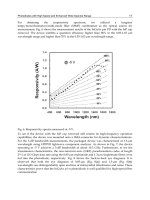
shorter the waveguide, the broader the spectral response bandwidth. Fig. 9 (a) shows the
spectral response measured experimentally for the 1-cm PPLN waveguide. Its 3-dB
bandwidth is about 1.3 nm, which is about 5 times wider than that of the 5-cm PPLN
waveguide (0.25 nm) [Ma et al. 2009]. In this experiment the wider bandwidth allows two
pumps, at wavelengths 1549.2 nm and 1550.0 nm, to operate with almost the same
conversion efficiency, which is about 85% of the maximum conversion efficiency.
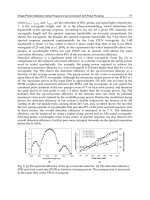
Detection efficiency is a significant trade off for a short waveguide. From Eq. (3), to
compensate for the reduced conversion efficiency in a shorter waveguide the pump power
must be scaled quadratically. For example, the pump power required to achieve the
maximum conversion efficiency in a 1-cm waveguide is 25 times higher than that for a 5-cm
waveguide. Fig. 9(b) shows the detection efficiency of the up-conversion detector as a
function of the average pump power. The pump power on the x-axis is measured at the
input fiber of the PPLN waveguide. Although the maximum output power of the EDFA is 1
W, the maximum power at the input fiber is approximately 510 mW due to losses in the
WDM couplers and connectors between the EDFA and the waveguide. In our system the
combined pulse duration of the two pumps covers 67% of each clock period, and therefore
the peak power of each pulse is only 1.5 times higher than the average power. Fig. 9(b)
indicates that the up-conversion efficiency of the detector does not reach its potential
maximum value and is limited by the available pump power. Besides the insufficient pump
power, the detection efficiency in our system is further reduced by the absence of an AR
coating on the waveguide ends, causing about 26% loss, and, as stated above, the fact that
the two pumps operate at wavelengths that provide 85% of the peak spectral response. Due
to these factors, the overall detection efficiency is measured to be 7 %. The detection
efficiency can be improved by using a higher pump power and an AR-coated waveguide.
Selecting pump wavelengths closer to the center of spectral response can also improve the
overall detection efficiency, but this puts more stringent demands on the spectral separation
before the Si APDs.
Fig. 9. (a) The spectral efficiency of the up-conversion detector. (b) The detection efficiency
(DE) and dark count rate (DCR) as function of pump power. The pump power is measured
in the input fiber of the PPLN waveguide.
Photodiodes – Communications, Bio-Sensings, Measurements and High-Energy
72
Similar to other single photon detectors, the dark counts of this detector is caused by the
anti-Stokes components of SRS in this waveguide and the intrinsic dark counts of Si APD.
The SRS photons are generated over a broad spectrum, while the up-converted signal can be
quite narrow. To further reduce the noise count rate, it is beneficial to use a bandpass filter
with a very narrow bandwidth behind the waveguide. As stated above, in this experiment
the iris in front of the Si APDs and the holographic grating constitute a band-pass filter with
a bandwidth of about 0.4 nm. From Fig. 9 (b), the total dark count rate of the two Si APDs in
the up-conversion detector are approximately 240 and 220 counts per second, respectively,
at the maximum pump power.
3.2 Increasing transmission rate of a communication system
For a quantum communication system, inter-symbol interference (ISI) can be a significant
source of errors. ISI can be caused by timing jitter of single photon detectors, and to avoid a
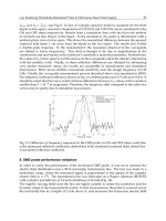
high bit-error rate, the transmission data cycle should be equal to or larger than the FW1%M
of the response histogram. For the 220-ps signal pulse used in our system, the response
histogram of an up-conversion detector with a single wavelength pump is shown in Fig. 10
(black). The FW1%M of the histogram is about 1.25 ns and this detection system can
therefore support a transmission rate of 800 MHz. When such a detection system is used to
detect a 1.6 GHz signal, the insufficient temporal resolution of the detector results in severe
ISI, as indicated by the poor pulse resolution, shown in Fig. 10 (grey). The application of
optical sampling with two spectrally and temporally distinct pump pulses and a separate Si
APD for each pump wavelength, as described above, accommodates the 1.25-ns FW1%M of
each individual pump channel but supports an overall transmission rate of 1.6 GHz with
low ISI. Fig. 11 (a) show the response histogram of each APD in the optical-sampling up-
conversion system for a repetitive signal pattern “11111111”. For each APD, the detection
window is larger than FW1%M of APD response, so the ISI is greatly diminished. To
illustrate both the temporal demultiplexing and the ISI in this system, Fig. 11 (b) shows the
response histogram of each of the two APDs for a repetitive signal pattern “10010110”. The
0.001
0.01
0.1
1
012345
Time (ns)
Normalized Counts
FW1%M
1.25 ns
Fig. 10. Response histogram of the up-conversion detector with a single pump wavelength.
The response histogram of single pulse (black) shows the FW1%M is 1.25 ns and its
temporal resolution is insufficient to resolve, with low ISI, the repetitive data pattern
“11111111” at 1.6 GHz (grey).
Single Photon Detection Using Frequency Up-Conversion with Pulse Pumping
73
APD 1 receives the signal at odd time bins, resulting in the pattern “1001” and APD 2
receives the signal at even time bins resulting in the pattern “0110”, and the original signal
can be reconstructed from the data recorded by the two APDs. To measure the ISI in the
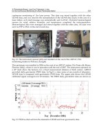
optical sampling up-conversion system under conditions found in a typical QKD system we
also drove the signal with a 1.6 Gb/s pseudo-random data pattern. After comparing the
received data to the original data, the error rate was found to be approximately 1.2 %.
Subtracting the error rate caused by the imperfect extinction ratio of the modulator and the
intrinsic dark counts of APDs, the error rate caused by ISI is less than 1%.
Fig. 11. Response histogram of the up-conversion detector with two spectrally and
temporally distinct pump pulses (a) response histogram of APD 1 and APD 2, for a
repetitive signal pattern “11111111” at 1.6 GHz. (b) response histogram of APD 1 and
APD 2, for a repetitive data pattern 10010110 at 1.6 GHz.
The above experimental results demonstrate that an up-conversion single-photon detector
with two spectrally and temporally distinct pump pulses can operate at transmission rates
that are twice as fast as can be supported by its constituent APDs. Further sub-division of
the APD’s minimum resolvable period (e.g. the FW1%M) is possible with more pump
wavelengths and a corresponding number of Si APDs, allowing further increases in the
maximum supported transmission rate of the single-photon system. However, the ability to
increase the temporal resolution is ultimately limited by the phase-matching bandwidth of
the nonlinear waveguide and available pump power.
Photodiodes – Communications, Bio-Sensings, Measurements and High-Energy
74
Fourier analysis shows that shorter pulse duration corresponds to a broader frequency
bandwidth. Considering only transform limited Gaussian pulses, the relationship between
the pulse duration and spectral bandwidth for such “minimum uncertainty” pulses is given
by [Donnelly and Grossman, 1998]:
4ln(2)
FWHM FWHM
t
, (6)
where
FWHM
t and
FWHM
are the FWHM of temporal width and frequency bandwidth,
respectively. For the pump wavelengths in our experiment (~1550 nm), pulse widths shorter
than 3 ps correspond to frequency bandwidths larger than 1.2 nm, which covers most of the
3-dB quasi-phase matching bandwidth of our 1-cm PPLN waveguide and thus precludes
any other up-conversion pump wavelengths. A 100-ps pump pulse corresponds to a
transform-limited bandwidth of 0.035 nm, in which case the waveguide used in our
experiment could support more than 10 pump channels with greater than 50% quasi-phase
matching efficiency. In this case, its temporal resolution can be increased by one order-of-
magnitude compared to an up-conversion detector with just one pump wavelength. To
provide uniform detection efficiency across all temporal regions, the pump power can be
reduced in the well-phase-matched regions to match the conversion efficiency in the
outlying spectral regions.
As the pump wavelengths become closer together, or if a shorter nonlinear waveguide is
used to increase the quasi-phase matching bandwidth, technical issues associated with
obtaining high optical powers in each pump, and efficient spectral separation of the up-
converted photons become significant. We note that novel nonlinear crystal structures, such
as chirped gratings or adiabatic gratings [Suchowski et al. (2010)] can provide broad
bandwidth and relatively high conversion efficiency. With these new technologies, we
believe it is reasonable to consider an up-conversion single-photon detector using spectrally
and temporally distinct pump pulses with temporal resolution better than 10 ps. It should
be noted that this scheme is not only suitable for up-conversion detectors using Si APDs;
other single-photon detectors with better temporal resolution, such as SSPDs, can also be
integrated into the scheme for further improvement of their temporal resolution.
4. Conclusion
Frequency up-conversion single photon detector technology is an efficient detection
approach for quantum communication systems at NIR range. Traditionally, an up-
conversion single photon detector uses CW pumping at a single wavelength. In CW pump
mode, the pump power is usually set at a level where the conversion efficiency is the
highest. In that case, the noise counts caused by the SRS in the waveguide might induce
high error rates in a quantum communication system. An up-conversion single photon
detector with a pulsed pump can reduce the noise count rate while maintaining the
conversion efficiency. Furthermore, in a CW pump mode, the temporal resolution is
determined by the timing jitter of the Si APD used in the detection system. A multiple
wavelength pumping technique adds a new wavelength domain into the upconversion
process. The data detected within a period of the Si APD’s time jitter can be projected into
the wavelength domain so that the spectrally and temporally distinct pulse pumping
increases both the temporal resolution and the system data transmission rate.
Single Photon Detection Using Frequency Up-Conversion with Pulse Pumping
75
5. Acknowledgement
The authors would like to thank for the support from NIST Quantum Information Initiative.
The authors also thank Dr. Alan Mink, Dr. Joshua C. Bienfang and Barry Hershman for their
supports and discussions.
6. References
Bennett, C. H. (1992). Quantum cryptography using any two nonorthogonal states. Phys.
Rev. Lett.
, Vol. 68, pp 3121-3124
Diamanti, E.; Takesue, H.; Honjo, T.; Inoue, K. & Yamamoto, Y. (2005). Performance of
various quantum-key-distribution systems using 1.55-μm up-conversion single-
photon detectors.
Phys. Rev. A, Vol. 72, 052311
Donnelly, T. D. and Grossman, C. (1998) Ultrafast phenomena: A laboratory experiment for
undergraduates.
Am. J. Phys. Vol. 66, pp 677-685
Fejer, M.; Magel, G.; Jundt, D. & Byer, R. (1992). Quasi-phase-matched second harmonic
generation: tuning and tolerances. IEEE J. Quantum Electron. Vol.28, pp 2631-2654
Gol’tsman, G. N.; Okunev, O.; Chulkova G.; Lipatov, A.; Semenov, A.; Smirnov, K.;
Voronov, B. & Dzardanov, A. (2001). Picosecond superconducting single-photon
optical detector.
Appl. Phys. Lett. Vol. 79, pp 705-707
Hadfield, R. (2009). Single-photon detectors for optical quantum information applications,
Nat. Photonics, Vol. 3, pp 696-705
Hamamatsu. (2005). Near infrared photomultiplier tube R5509-73 data sheet.
Langrock, C.; Diamanti, E.; Roussev, R. V.; Yamamoto, Y.; Fejer, M. M. & Takesue, H. (2005).
Highly efficient single-photon detection at communication wavelengths by use of
upconversion in reverse-proton-exchanged periodically poled LiNbO3
waveguides.
Opt. Lett. Vol. 30, pp. 1725-1727
Ma, L., Slattery, O. and Tang, X. (2009) Experimental study of high sensitivity infrared
spectrometer with waveguide-based up-conversion detector.
Opt. Express Vol 17,
pp 14395–14404.
Martin, J. & Hink P. (2003) Single-Photon Detection with MicroChannel Plate Based Photo
Multiplier Tubes.
Workshop on Single-Photon: Detectors, Applications and Measurement
Methods, NIST
.
Mink, A.; Tang, X.; Ma, L.; Nakassis, T.; Hershman, B.; Bienfang, J. C.; Su, D.; Boisvert, R.;
Clark, C. W. & Williams, C. J. (2006). High speed quantum key distribution system
supports one-time pad encryption of real-time video.
Proc. of SPIE, Vol. 6244,
62440M,
Mink, A., Bienfang, J., Carpenter, R., Ma, L., Hershman, B., Restelli, A. and Tang, X. (2009)
Programmable Instrumentation & GHz signaling for quantum communication
systems.
N. J. Physics, Vol. 11: 054016,
Pelc, J. S., Langrock, C., Zhang, Q. and Fejer, M. M. (2010) Influence of domain disorder on
parametric noise in quasi-phase-matched quantum frequency converters.
Opt. Lett.,
Vol. 35, pp 2804-2806
Restelli, A., Bienfang, J. C., Mink, A. and Clark, C. (2009) Quantum key distribution at GHz
transmission rates.
Proc. of SPIE Vol. 7236, 72360L,
Smith, R. G. (1972) Optical power handling capacity of low loss optical fibers as determined
by stimulated Raman and Brillouin scattering.
Appl. Opt. Vol. 11, pp. 2489-2494
Photodiodes – Communications, Bio-Sensings, Measurements and High-Energy
76
Suchowski, H., Bruner,B. D., Arie, A. and Silberberg, Y. (2010) Broadband nonlinear
frequency conversion.
OPN Vol. 21, pp 36-41
Tanzilli, S.; Tittel, W.; Halder, M.; Alibart, O.; Baldi, P.; Gisin, N. & Zbinden, H. (2005). A
photonic quantum information interface.
Nature, Vol 437, pp 116-120
Thew, R. T.; Tanzilli, S.;, Krainer, L.; Zeller, S. C.; Rochas, A.; Rech, I.; Cova, S.; Zbinden, H.
& Gisin, N. (2006). Low jitter up-conversion detectors for telecom wavelength GHz
QKD.
New J. Phys. Vol. 8, pp 32.
Vandevender, A. P. & Kwiat, P. G. (2004). High efficiency single photon detection via
frequency up-conversion.
J. Mod. Opt., Vol. 51, 1433-1445
Wiza, J. (1979). Microchannel plate detectors.
Nuclear Instruments and Methods Vol. 162: pp
587-601
Xu, H.; Ma, L.; Mink, A.; Hershman, B. & Tang, X. (2007). 1310-nm quantum key distribution
system with up-conversion pump wavelength at 1550 nm.
Optics Express, Vol 15,
No.12, pp 7247- 7260
Part 2
Photodiode for High-Speed
Measurement Application
Hamidreza Memarzadeh-Tehran, Jean-Jacques Laurin and Raman Kashyap
École Polytechnique de Montréal
Department of Electrical Engineering
Montreal, Canada
1. Introduction
The space surrounding a radiating or scattering object is often divided into three regions,
namely reactive near-field, near-field (NF) or Fresnel region and far-field (FF) or Fraunhoffer
zones. In addition, the term “very-near-field" region is sometimes defined as very close to the
antenna (e.g., antenna aperture). There are no abrupt boundaries between these three zones,
however there are some commonly used definitions. For antennas with a size comparable
to the wavelength (λ), the NF to FF boundary is calculated as r
≈ 2D
2
/λ , where D is the
maximum dimension of the radiating device and r is the distance between the device and
observation point.
The most widespread use of near-field measurement is in antenna diagnostics. In this
case, fields are sampled near the antenna, typically in the Fresnel region, and a NF-to-FF
transformation is used to obtain the radiation patterns (Petre & Sarkar, 1992). Rather than
extrapolating away from the antenna, another possible application consists of reconstructing
the field and current on the radiating device. This may require sampling within the reactive
near-field region, i.e., with r
< λ. Such in-situ near-field diagnostics have been made on
antennas (Laurin et al., 2001), microwave circuits (Bokhari et al., 1995) and device emissions
(Dubois et al., 2008). They can also be used to measure the wave penetration into materials
and their radio-frequency (RF) characterization purposes (Munoz et al., 2008). Dielectric
properties reconstruction (Omrane et al., 2006) is another use of NF measurement. Measuring
the coupling between components of microwave circuits (Baudry et al., 2007), calculating
FF radiation pattern of large antennas (Yan et al., 1997), and testing for electromagnetic
compatibility EMC (Baudry et al., 2007) and EMI (Quilez et al., 2008) are among the other
uses of NF measurement.
1.1 Statement of the problem— Obtaining accurate NF distribution
In applications such as the source or dielectric properties reconstruction, an ill-posed inverse
problem has to be solved. The solution process is highly sensitive to noise and systematic
measurement error. Accurate and sensitive NF measurement systems therefore need to be
designed and implemented. Typically, NF imagers suffer from three important issues: limited
accuracy and sensitivity, long measurement durations and reduced dynamic ranges, all of
which depend on the measuring instruments and components used.
Low Scattering Photodiode-Modulated Probe
for Microwave Near-Field Imaging
5
2 Photodioes
1.2 Modulated Scatterer Technique (MST)—An accurate approach for NF imaging
The distribution of near fields can be acquired using a direct (Smith, 1984) or an indirect (Bassen
& Smith, 1983) technique. In the direct methods a measuring probe connected to a transmission
line (e.g., coaxial cable) scans over the region of interest. The transmission line carries
the signals picked-up by the probe to the measurement instruments. The major drawback
associated with such technique is the fact that the fields to be measured are short-circuited on
the metallic constituents of the transmission line. Multiple reflections may also occur between
the device under test (DUT) and the line (Bolomey & Gardiol, 2001) resulting in perturbed
field measurement. Moreover, flexible transmission lines such as a coaxial cables, which
are widely used in microwave systems, do not always give accurate and stable magnitude
and phase measurements (Hygate, 1990). This phenomenon in turn leads to inaccurate
measurement, particularly where the measuring probe has to scan a large area. In contrast,
indirect methods (Justice & Rumsey, 1955) are based on scattering phenomenon and require
no transmission lines. Instead, a scatterer locally perturbs the fields at its position and the
scattered fields are detected by an antenna located away from the region of interest, so as to
minimize perturbation of the fields. This antenna could be the DUT itself (i.e., monostatic
mode, in which case the signal of interest appears as a reflection at the DUT’s input port)
or an auxiliary antenna held remotely (i.e., bistatic mode). The variations of the received
signals induced by the scatterer are related to the local fields at the scatterer’s positions and
are interpreted as the field measurement (magnitude and phase) by means of a detector. The
indirect method employs a scatterer which is reasonably small, does not perturb the radiating
device under test but is sufficiently large so that it is able to perturb the field up to the system’s
measurement threshold. Thus, a trade-off has to be made between accuracy and sensitivity.
The indirect method suffers from limited dynamic range and sensitivity (King, 1978).
To overcome the drawbacks mentioned above, a technique known as the modulated scatterer
technique (MST) was proposed and developed. MST was addressed and generalized by
Richmond (Richmond, 1955) to remedy the drawbacks of both the direct and indirect methods.
Basically, it consists of marking the field at each spatial point using a modulated scatterer,
which is called the MST probe (Bolomey & Gardiol, 2001). This technique brings some
outstanding advantages in the context of NF imaging such as eliminating the need to attach
a transmission line to the measuring probe and improving the sensitivity and dynamic range
of the measurement. From the point of view of probe implementation, tagging the field
(modulation) can be done either electrically (Richmond, 1955), optically (Hygate, 1990), and
sometimes, mechanically (King, 1978). Unlike optical modulation, the other modulation
techniques somehow show the same disadvantages as the direct method. In an electrically
modulated scatterer a pair of twisted metallic or resistive wires carry modulation signals
to the probe. The presence of these wires may perturb the field distribution near the DUT,
resulting in inaccurate measurements, whereas in an optically modulated scatterer (OMS) the
modulating signal is transferred with an optical fiber that is invisible to the electromagnetic
radio-frequency signal (Hygate, 1990). Thus, it can be assumed that it will only weakly
influence the DUT’s field distribution to be measured.
In this chapter, the design and implementation of a NF imager equipped with an array of
optically modulated scatterer (OMS) probes that is able to overcome the drawbacks associated
with the conventional direct and indirect methods are addressed. Additionally, a method
to improve the dynamic range of the NF imager using a carrier cancellation technique is
discussed.
80
Photodiodes – Communications, Bio-Sensings, Measurements and High-Energy Physics
Low Scattering Photodiode-Modulated Probe For Microwave Near-Field Imaging 3
2. Photodiode-loaded MST probe— Optically modulated scatterer
An OMS probe includes a small size antenna loaded with a light modulated component. The
modulation signal is carried by an optical fiber coupled to the photoactivated component.
It is switched ON and OFF at an audio frequency causing modulation on the antenna
load impedance, which results in a corresponding modulation of the fields scattered by the
probe. In the bistatic configuration the scattered field is received by an auxiliary antenna,
as illustrated in Fig. 1. In the monostatic case the antenna under test is used to receive the
modulated signal. In the following, the design and implementation of an optically modulated
scatterer (OMS) is explained and discussed. Criteria for antenna type and modulator selection,
tuning network design and implementation, and an OMS probe assembly will be also covered.
Finally, the probe is characterized in terms of sensitivity, accuracy, and dynamic range.
OMS probe
Modulation si
g
nal
: Modulation
: Carrier frequency
AUT
(Transmit antenna)
Carrier signal
Modulated signal
Receiving antenna
(Auxiliary Antenna)
To homodyne receiver
Fig. 1. Schematic of an MST-based NF imager in bistatic mode.
2.1 Antenna type
In practice, there is a limited number of antenna types that can perform as MST probes.
Dipoles, loops, horns and microstrip antennas have been reported. The leading criterion to
select the type of antenna is to keep the influence of the probe on the field to be measured as
small as possible. The concept of a “minimum scattering antenna" (MSA) provides us with an
appropriate guideline for selecting the scattering antenna. Conceptually, an MSA is invisible
to electromagnetic fields when it is left open-circuited (Rogers, 1986) or connected to an
appropriate reactive load (Iigusa et al., 2006). The horn and microstrip antennas do not fulfill
MSA requirements due to their bulky physical structures and large ground plane, respectively,
which cause significant structural-mode scattering regardless of antenna termination. The
short-dipole (length
< λ/10) and small-loop approach the desired MSA characteristics. A
dipole probe might be a better choice because of its simpler structure. Moreover, a loop probe
may measure a combination of electric and magnetic fields if it is not properly designed (King,
1978).
2.2 Modulator selection criteria
From the concept of AM modulation, we can introduce modulation index m as the ratio of
the crests (1+μ) and troughs (1-μ) of the modulated signal envelope, where μ is the level of
AM-modulation (King, 1978). Therefore, m can be defined as:
81
Low Scattering Photodiode-Modulated Probe for Microwave Near-Field Imaging
4 Photodioes
m =
crest − troug h
crest + troug h
(1)
Assuming two states of the modulator with load impedance Z
ON
and Z
OFF
, and a probe
impedance Z
p
=Z
dip ole
+Z
tn
, where Z
tn
stands for the tuning network impedance
1
, the
modulation index of the signal scattered by the probe is given by (King, 1978):
m
=
|
Z
p
+ Z
ON
|−|Z
p
+ Z
OFF
|
|Z
p
+ Z
ON
|+ |Z
p
+ Z
OFF
|
(2)
whereas the ratio of the currents flowing in the probe terminals in both states is given by:
CR
≡
|
I
ON
|
|I
OFF
|
=
|
Z
p
+ Z
OFF
|
|Z
p
+ Z
ON
|
(3)
We can thus write:
m
=
1 −CR
1 + CR
(4)
If a small resonant probe is used, the real and imaginary parts of Z
p
can be made very small,
and possibly negligible compared to Z
ON
and Z
OFF
, such that:
m
≈
|
Z
ON
|−|Z
OFF
|
|Z
ON
|+ |Z
OFF
|
CR ≈
|
Z
OFF
|
|Z
ON
|
(5)
The maximum possible magnitude of the modulation index occurs when CR
= 0(m = 1) or
CR
→ ∞ (m = −1). Ideally, it is desired to maximize |m|in order to have the strongest possible
sideband response for a given level of a measured field. The selected modulated load should
have either
|Z
ON
||Z
OFF
| or |Z
OFF
||Z
ON
|. In other words, input impedance of the
device in the ON and OFF states should differ significantly. The results that will be presented
in the next sections were obtained with probes based on a photodiode manufactured by
Enablence (PDCS30T). This device was selected due to its high impedance variation as a
function of input light level at a target test frequency of 2.45 GHz. The input impedance
of the photodiode was measured on a wafer probing station using a calibrated Agilent 8510C
vector network analyzer for different optical power levels (no light, and with a sweep from
-10 dBm to 13 dBm) in the 2-3 GHz frequency range. The optical power in this measurement,
was applied to the photodiode via an optical fiber, which was held above its active area by an
accurate x-y positioning device.
Fig. 2a shows the impedance magnitude, revealing saturation for light power greater than +6
dBm (NB. In this figure we use the following definition dBΩ
≡ 20log
10
Ω). The impedance
of the diode in the "no-light" or OFF state and +6 dBm or ON state is shown in Fig. 2b. The
diode can be modelled approximately by a series RC circuit, with R
OFF
= 38.8Ω and C
OFF
=
0.31pF. In the ON state, a similar model with R
ON
= 15.8Ω and C
ON
= 13.66pF can be
assumed. These models are approximately valid in a narrow frequency band centered at
2.45GHz. According to Equation 3, at 2.45 GHz these measured data lead to CR=13.38 (22.5
dB) and m
= −0.86.
1
It is assumed that this network consists of a series reactance in this example but other topologies are of
course possible.
82
Photodiodes – Communications, Bio-Sensings, Measurements and High-Energy Physics
Low Scattering Photodiode-Modulated Probe For Microwave Near-Field Imaging 5
It is worth mentioning that the model used for this photodiode (i.e., series RC connection), it
is only valid for small-signal operation. The photodiode switch-ON and breakdown voltages
are 1.5 V and 25 V respectively. In addition, the maximum optical power should not exceed
10 dBm to prevent nonlinear operation.
(a) (b)
Fig. 2. (a) Input impedance magnitude of the photodiode (PDCD30T manufactured by
Enablence), and (b) Input impedance (normalized to 50Ω) of the photodiode chip in the 2-3
GHz range with and without illumination. The measurement results and those obtained with
a model of the photodiode are compared.
2.3 Selection of OMS probe length
Usually, the scatterer (i.e., OMS probe) should have minimum interaction with the source of
the fields to be measured. The dynamic range of the measurement system depends on the
minimum and maximum field levels the probe is able to scatter, and the detection threshold
and saturation level of the receiver. Achieving a high dynamic range necessitates using a
larger scatterer at the expense of oscillations in field measurements and deviation from the
true field. In general for electrically small probes, the smaller the dimension of the scatterer
the smaller the expected disturbance, but at the cost of lower sensitivity. Smaller probes also
lead to better image resolution. Thus, a trade-off has to be made between the dynamic range
on one side and the resolution and sensitivity of the probe on the other side. The first MST
dipole probe reported by Richmond (Richmond, 1955) had a length of 0.31λ. Liang et al.
used a length ranging between 0.05λ-0.3λ in order to make fine and disturbance-free field
maps (Liang et al., 1997). Measured electromagnetic fields were also reported in (Budka et al.,
1996) for operation in the 2-18 GHz band using MST probes that are 150 μm, 250 μm, and
350 μm long. A length of 8.3 mm was used by Hygate (Hygate, 1990) for signals below 10
GHz. Nye also used 3 mm and 8 mm MST probes at f=10 GHz to obtain NF maps of antennas
or any passive scatterers (Nye, 2003). The probe presented here has a length of λ/12 at a
design frequency of 2.45 GHz. The impedance of the printed short dipole at this frequency, as
obtained by method of moment, is Z
p
= 1.22 − j412Ω.
In order to ensure that a λ/12 dipole probe not only meets the requirements of MSA but
also has a negligible influence on the field to be measured, let us consider the measurement
83
Low Scattering Photodiode-Modulated Probe for Microwave Near-Field Imaging
6 Photodioes
mechanism by MST probe using a network approach, as demonstrated in Fig. 3. The AUT in
this figure acts as a radiating source and also a collecting antenna (i.e., port #1), and the scatter
represents a measuring probe which is loaded with Z
L
at port #2 (e.g., input impedance of the
modulator) (King, 1978). Using of the impedance matrix of the passive network we can write:
-
Scatterer
I2
V2
ZL
+
-
AUT
(Source)
I
1
V1
+
V1
I1
V2
I2
ZL
Z11 Z12
Z21 Z22
Fig. 3. Modelling of measurement mechanism using network approach, monostatic
implementation.
V
1
= Z
11
I
1
+ Z
12
I
2
(6)
V
2
= Z
21
I
1
+ Z
22
I
2
(7)
The current induced in the probe (i.e., I
2
) yields a voltage V
2
= −I
2
Z
L
on port 2. One can
obtain Equation 8 by solving Equation 7 for V
1
:
V
1
=
Z
11
−
Z
12
Z
21
Z
22
+ Z
L
I
1
(8)
It is also assumed that the voltage on port 1 in the absence of the scatterer is given by V
0
1
=
Z
0
11
I
1
, where Z
0
11
is the input impedance of the AUT. Then, by subtracting it from Equation 8,
it yields,
V
1
−V
0
1
= ΔV
1
=
(Z
11
− Z
0
11
) −
Z
12
Z
21
Z
22
+ Z
L
I
1
(9)
It has been assumed that current I
1
fed to the AUT is unchanged in the two cases. Based on
Equation 9, it can be shown that the measuring probe has two separate effects at the receiver’s
voltage, namely, the effect due to its physical structure (i.e., structural mode) and its loading
(i.e., antenna mode). On the right hand side, the first term is present even when the probe is
left open-circuited (i.e., when Z
L
→ ∞), that results from the probe’s structural mode. The
second term appears when the probe loading (i.e., Z
L
) is finite or zero, allowing current to
flow in port 2. This contribution is therefore called the antenna mode. Only the latter term
is modulated in MST-based probes. The first term is present and varies when the probe is
moved from one measurement point to another but those variations are slow compared to
the rate of modulation. It can thus be assumed that they will not affect the measurement at
the modulation frequency. By considering an open-circuited scatterer (i.e., Z
L
→ ∞), ΔV
1
84
Photodiodes – Communications, Bio-Sensings, Measurements and High-Energy Physics
Low Scattering Photodiode-Modulated Probe For Microwave Near-Field Imaging 7
gives (Z
11
− Z
0
11
)I
1
; this represents the variation of the induced voltage across the AUT’s
terminal compared to the case in absence of the scatterer. Ideally, it is expected that ΔV
1
will
vanish for MSA antennas, i.e., structural mode radiation is vanishingly small. Now, in order to
Fig. 4. AUT impedance variation due to the probe structural modes, as a function of the
probe length.
investigate whether the chosen length (i.e., λ/12) for the OMS probe fulfills the requirements
of the MSA antenna, we performed a simulation in Ansoft HFSS, a 3D full wave finite element
solver, wherein, a planar dipole with a length of L
= 10mm, width of w = 1mm and a center
gap of g
= 100μm was considered. The dipole was positioned in front of the aperture of a
horn antenna operating at a test frequency of 2.45 GHz. Then, the value of Δ =
Z
11
−Z
0
11
Z
0
11
versus
the length for probe was calculated. The results plotted in Fig. 4 show that Δ varies by less
than 1.5% for probes shorter than 0.15λ. Therefore, an OMS probe consisting of a short dipole
with length of λ/12 can be considered as a good MSA when it is used to characterize this horn
antenna.
2.4 Tuning network design
As shown in (King, 1978), scattering by the probe can be increased by adding an inductive
reactance in series with the capacitive short-dipole (i.e., Z
p
= Z
dip ole
+ jωL) so that a resonance
occurs in one of the two states. The inductance value should be chosen such that the
numerator or the denominator in Equation 3 is minimized, leading to an increased modulation
index. This effect, however, is frequency selective.
The value of the inductance should make the loaded short dipole resonant when the light is
ON (denominator of Equation 3 minimized) and increase its impedance when the light is OFF
(or vice versa). To find the optimum inductance value, one may try to maximize CR. Fig. 5
represents CR versus inductance. The inductance of 25 nH associated with the peak in the
curve is referred to as the optimal point of the tuning network and it can be seen that the
maximum CR is close to the estimated value 22.5 dB calculated in Section 2.2. The minimum
of CR near L
= 42nH also leads to a local maximum of |m| but it is not as high.
85
Low Scattering Photodiode-Modulated Probe for Microwave Near-Field Imaging
8 Photodioes
Fig. 5. Current ratio versus the inductance value used for tuning.
3. Matching network impact on the OMS probe performance
The impact of the tuning network on the probe performance is presented here. The difference
between the scattered field when the dipole is in ON and OFF states (i.e. Z
OFF
= 38.8 −
j206.2Ω and Z
ON
= 15.9 − j4.8Ω) at 2.45 GHz was calculated versus frequency for two cases:
with and without considering a tuning network in an OMS probe structure. To do this, a
method of moment code was developed to calculate the ON and OFF states scattered field in
the 1-4 GHz frequency range.
(a)
Photodiode
Z
Spiral inductor
Matching Network
d
w
d
s
d
w
d
s
Short-dipole
(Printed circuit)
Dipole
Z
OC
V
Incident wave
Equivalent
circuit
(b)
Fig. 6. (a) Schematic depicting the equivalent circuit of the OMS probe, wherein R
d
= 1.22 Ω,
C
d
= 0.15 pF, R
p
(ON)=15.85 Ω, C
p
(ON)=13.65 pF, R
p
(OFF)=38.78 Ω,
C
p
(OFF)=0.31 pF and L1 = L2 = 12.7 nH, and (b) Matching network for the proposed
OMS probe (d=0.99 mm, s=63.5 μm and w=50.8 μm). Dipole length: 1 cm. Drawing is not to
scale.
In this model (see Fig. 6a), the scattered field was calculated 1 cm away from the dipole
when a uniform plane wave illumination is considered. The results shown in Fig. 7 exhibits a
significant improvement of about 23 dB in scattered field when the tuning network is added.
As a consequence, the sensitivity of the OMS probe is significantly improved. The two peaks
on the solid curve correspond to resonances that occur in the ON and OFF states of the OMS
probe.
86
Photodiodes – Communications, Bio-Sensings, Measurements and High-Energy Physics
Low Scattering Photodiode-Modulated Probe For Microwave Near-Field Imaging 9
0.5 1 1.5 2 2.5 3 3.5 4 4.5 5
x 10
9
-70
-60
-50
-40
-30
-20
-10
Frequency in Hz
Magnitude in dB
Scattered field - matching network
Scattered field - No matching network
Fig. 7. Frequency response of an OMS probe: Solid line probe with tuning network and
dashed line probe without tuning network.
4. OMS probe fabrication
The OMS probe was fabricated on a thin ceramic substrate (alumina) with a thickness of 250
μm, a relative permittivity of 10.2 and tanδ
= 0.004. An optical fiber is coupled to the active
surface of the photodiode using a precision positioning system by monitoring photo-induced
DC current while the fiber is moved to find the optimal position. Finally, the fiber is
permanently fixed by pouring epoxy glue when in the position corresponding to the current
peak. In addition, in order to prevent any damage to the coupling by mishandling the probe,
a strain relief structure made of a low permittivity material (
r
≈ 2.7) is added. Fig. 8 shows
the photograph of the completed probe assembly. The dimensions of the ceramic substrate are
7 mm and 15 mm. The tuning element is implemented with two spiral inductors (see Fig. 6b).
Each inductor occupies an area of 1mm
×1mm. The photodiode area is 0.2mm
2
. Wire-bonding
provides the electrical contacts between the photodiode and the inductor terminals on the
substrate.
(a) 3D view (b) Top view
Fig. 8. Photograph of the implemented OMS probe.
87
Low Scattering Photodiode-Modulated Probe for Microwave Near-Field Imaging
10 Photodioes
5. Validating the fabrication process
Once the OMS probe is fabricated, including fiber coupling, it is necessary to verify whether
it operates at the frequency at which it was designed. As the photodiode saturates at an input
power of +6 dBm (see Fig. 2), no further modulation index change is anticipated beyond this
point.
The OMS probe was tested by exposing it to a constant power electric field (e.g., near a horn
antenna or microstrip transmission line) at 2.45 GHz. An optical signal (waveguide of 1.3 μm)
modulated at
∼100KHz with a power between -10 dBm to 13 dBm was applied to the OMS
probe. The sidebands were recorded during this measurement at the input port of the horn
using a spectrum analyzer. Fig. 9 illustrates the results obtained by this experiment. It can be
seen that the level of the sidebands (normalized to its maximum) increases linearly with the
optical power when it is smaller than +6 dBm. As expected, beyond this limit the probe is not
able to scatter more fields. This test not only confirms that the probe is operating at a desired
working point but it also shows the quality of the fiber/photodiode coupling.
−10 −5 0 5 10
−15
−10
−5
0
Input optical power to OMS probe (dBm)
Normalized sideband level in dB
+6dBm
Saturation level
Fig. 9. Variation of sideband power level (dB) versus input optical power (dBm) to the OMS
probe.
6. Omnidirectional and cross-polarization characterization
6.1 Omnidirectional response
A desirable feature for a near-field probe is to be able to measure a specific component of
the E or H field. In the case of a short dipole it is the component of the E field parallel to
the dipole axis, independently from the direction of arrival of the incoming wave(s). For a
thin-wire dipole, rotational symmetry of the response about the dipole axis is expected. In
practice the presence of a substrate, the flat strip geometry of the dipole and the presence of
the dielectric support structure break the symmetry. A detailed model of the probe including
these elements was simulated with Ansoft-HFSS as shown in Fig. 10a. In these simulations,
the probe is on the z-axis and centered at the origin. A near-field plot of E
z
(Co-pol.) and E
φ
(Cross-pol.) on a 36 mm circle and in plane z = 0 are shown in Fig. 10b. The probe operates
as a transmit antenna but the response in the receive mode is the same due to reciprocity. The
results show a fluctuation of less than 0.45 dB in the desired E
z
component, and very low level
of cross-polarization.
Rotational symmetry of the response was also studied experimentally with the setup shown
in Fig. 11a. In this case, the probe operates in the receiving mode and it is located near the
88
Photodiodes – Communications, Bio-Sensings, Measurements and High-Energy Physics
Low Scattering Photodiode-Modulated Probe For Microwave Near-Field Imaging 11
(a) Magnitude (b) Phase
Fig. 10. Schematic of the OMS probe when investigated for omnidirectivity characteristic.
Co-polarized (E
z
solid line) and Cross-polarization (E
φ
dashed line) radiation of the OMS
probe in the H-plane at a distance of 36 mm from the probe axis, as predicted by HFSS (the
data is normalized with respect to the maximum value of E
z
).
aperture of a transmitting horn antenna. The experiment was done by rotating the OMS probe
about its axis while recording the power levels of the sidebands on a spectrum analyzer. The
measured pattern at a distance of 12.2 cm ( one free-space wavelength) shown in Fig. 11b
exhibits a fluctuation of about 0.6 dB. The figure also shows simulation results obtained with
HFSS. In this case, the magnitude of the difference between the horn’s S
11
parameter, in the
absence and the presence of the rotated probe, is plotted. The experimental and simulated
curves were normalized to make the comparison easier. In the simulation results, the effect
of the dielectric substrate and support structure is barely perceptible. On the contrary, the
experimental curve does not exhibit such a good rotational symmetry, as a difference of 0.6
dB can be observed between the maximum and minimum values. It is believed that this
fluctuation may be due to mutual interactions between the probe rotation fixture and the horn
antenna, which were not taken into account in the simulations.
(a) (b)
Fig. 11. The setup for testing the omnidirectional performance of an OMS probe (a).
Measured radiation pattern in the probe H-plane at a distance of one wavelength from the
illuminating waveguide (magnitude in dB) (b).
89
Low Scattering Photodiode-Modulated Probe for Microwave Near-Field Imaging
12 Photodioes
6.2 Cross polarization
According to Fig. 10a, the cross-polarization of the OMS probe is give by Equation 10.
E
φ
= E
cross −pol.
= −E
x
sin(φ)+E
y
cos(φ) (10)
HFSS simulations predicts a cross-polarization rejection of more than 55 dB for the OMS probe.
To verify this result experimentally, the coupling between two identical open-ended WR-284
rectangular waveguides that face each other (Fig. 12) was measured. Although rectangular
waveguides already have very good on-axis cross-polarization rejection, it was further
improved by inserting a grid of parallel metal-strips (3 strips per cm) printed on a thin
polyimide substrate (thickness of 5 mil and a relative permittivity of 3.2). These polarizers
were mounted on the apertures of the transmit and receive waveguides. The strips, illustrated
on the Tx waveguide in Fig. 12, are oriented perpendicular to the radiated field. The Tx
waveguide did not show significant change of the return-loss after adding the polarizers.
In the experiment, the apertures were aligned and set one wavelength apart from each other.
Then, the OMS probe was mounted on a fixture made of foam transparent to microwaves
(
r
≈1) and was inserted between the aperture of the waveguide as illustrated in Fig. 12.
The setup operated in a bistatic mode, i.e. the sidebands generated by the OMS probe were
measured at the output port of the receive waveguide. Measurements were made with the
receive waveguide rotated about its axis by 0 and 90 degrees; the level of the sidebands
introduced by the probe changed by 60.55 dB. This should be considered as a lower bound
on the probe-induced cross-polarization, as the cross-polarization rejection of the polarizers is
not infinite in practice.
Fig. 12. Setup to measure co-to-cross polarization (E
φ
) rejection of the OMS probe (only one
of the polarizer sheets is shown for clarity).
7. OMS probe frequency response
The frequency response of the OMS probe was assessed by using it in a monostatic scheme.
The probe was inserted in a rectangular WR-284 rectangular waveguide and aligned with the
main component of the E-field. With the photodiode in the OFF state, the waveguide was
connected to a calibrated vector network analyzer through a 3-stub tuner that was adjusted to
give the minimum possible reflection coefficient (less than -65 dB) over the tested frequency
band. Then, an optical power level of +6 dBm was applied to drive the photodiode in the ON
state. The difference between the complex reflection coefficient at the tuner’s input port in
both states was then normalized to have the maximum at 0 dB. The results displayed in Fig. 13
show two peaks. It is believed that they are due to the different resonance frequencies of Z
p
+
90
Photodiodes – Communications, Bio-Sensings, Measurements and High-Energy Physics