New Perspectives in Biosensors Technology and Applications Part 2 potx
Bạn đang xem bản rút gọn của tài liệu. Xem và tải ngay bản đầy đủ của tài liệu tại đây (4.2 MB, 30 trang )
New Perspectives in Biosensors Technology and Applications
22
Fig. 20. Photo of the MEMS Faraday cup
Fig. 21. Photos of the MEMS Faraday cup packaged
5.4 Testing of the micro Faraday cup
For the MEMS Faraday cup chip packaged with PCB, a base should be fabricated to realise a
reliable connection between the MEMS Faraday cup and the ion source. The base is made of
red copper, which can effectively shield the noise from the environment. The photos of the
red copper shielding base, assembled MEMS Faraday cup and the ion source are shown in
figure 21.
In order to test the performance of the MEMS Faraday cup, the chip is tested with
KEITHLEY237. In this experiment, the carrier gas is nitrogen gas and the sample is acetone,
the concentration of which is about 100ppm. The experimental system is shown in figure 22.
V- 1
1
23
4
5
1 N
2
2 Flowmeter
3 UV ion source and sample cell
4 Micro-FCA
5 Electrometer
Fig. 22. Experimental apparatus of the MEMS Faraday cup
FAIMS Detection Technology Based on MEMS
23
(1) Ion collection experiment with the MEMS Faraday cup
In the experimental system of figure 22, the carrier gas flow is adjusted to 100L/h. We make
the comparison of the ion collection results among the chips of the MEMS Faraday cup with
different structural parameters. Through comparison of the signal, the absorption efficiency
of the MEMS Faraday cup with different structural parameters is evaluated.
Figure 23 shows a typical ion signal curve collected by the MEMS Faraday cup. This means
that the signal of the MEMS Faraday cup is stable, which can work in the atmospheric
environment, and is completely capable of detect ion.
0 50 100 150 200
0.00E+000
5.00E-011
1.00E-010
1.50E-010
2.00E-010
2.50E-010
Signal (A)
Sampling points
Fig. 23. Ion signal curve received by the MEMS Faraday cup
0 1020304050
-2.00E-013
-1.00E-013
0.00E+000
1.00E-013
2.00E-013
Signal(A)
Sampling Points
Without-Chip
Fig. 24. Noise in the body of KEITHLEY
(2) Anti-interference experiment
Shut off the carrier gas and apply the radio frequency voltage (the maximum is 300V and
the frequency is 200kHz) between the upper and lower electrodes in the front of the micro
New Perspectives in Biosensors Technology and Applications
24
Faraday cup. We test the influence of different shielding methods and different chip
structures on the ability of anti-interference.
First of all, in the case without the chip, we tested the background noise of the system with
KEITHLEY current testing module, as shown in figure 24. The average value of the noise
curve is 67.2fA. The offset current may be from the interference source in the environment
or the offset of the instruments. We have found biased data always from 40 to 80 fA in many
measurements. In the following data treatment, the biased current should be subtracted
from the original data.
1) The influence of RF electric field on the noise under different connection ways
The experimental results are shown in figure 25. In this experimental system, we found the
influence of the RF electric field and the copper shielding base on the noise of the chip is not
obvious. The level of the noise is about 0.1pA. It means that under this experimental system
setup there is no influence of different connections on the noise of the chip.
01020304050
-2.00E-013
-1.00E-013
0.00E+000
1.00E-013
2.00E-013
Signal(A)
Sampling Points
Without-Chip
With-RF-Without-Shield
With-RF-With-Shield
Without-RF-Without-Shield
Without-RF-With-Shield
Fig. 25. The noise level of the same chip under different connections. Note: corresponding
biased current has been subtracted in each curve.
2) Influence of different chip structures on the noise
Connecting ways and RF electric fields have no influence on the noise, so we have
conducted the noise test for the chip with different structural parameters, without the
copper shielding base and RF electric field.
It can be seen from the figure 26 that in this experimental system, whether or not the gate
electrode in the chips exists or the side wall of the drift regions and the side of the Faraday
cup are separated has no influence on the noise.
FAIMS Detection Technology Based on MEMS
25
01020304050
-3.00E-013
-2.00E-013
-1.00E-013
0.00E+000
1.00E-013
2.00E-013
3.00E-013
Signal(A)
Sampling Points
1
2
3
4
Fig. 26. Noise level with different chip structures. Note: 1) corresponding biased current has
been subtracted in each curve 2) Structure1: no gate electrode, the side wall of the drift
region is separated with the silicon side wall of the Faraday cup 3) Structure2: gate electrode
with three silicon columns, the side wall of the drift region is separated with the silicon side
wall of the Faraday cup 4) Structure3: gate electrode with five silicon columns, the side wall
of the drift region is separated with the silicon side wall of the Faraday cup 5) Structure4:
gate electrode with five silicon columns, the side wall of the drift region is connected with
the silicon side wall of the Faraday cup
6. Sample analytical experiment
6.1 Experimental system of FAIMS chip
The experimental system of FAIMS is composed of a sample injection unit, ion source,
FAIMS chip, square wave radio frequency power, and data collection unit, as shown in
figure 27. The sample injection unit contains the nitrogen tank, flowmeter and sample cell.
The ion source is composed of the ion source power and a 10.6eV ultraviolet lamp. The data
collection unit contains amperometer, compensation voltage data collection card and
computer.
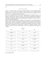
6.2 Influence of the changing of the square wave radio frequency voltage amplitude
on the sensitivity of FAIMS
We take absolute ethyl alcohol as the sample in this experiment. The flow velocity of the
carrier gas is 0.8L/min in this experiment, the square wave radio frequency voltage
frequency is 2MHz, and the duty ratio is maintained at about 30%. The amplitude of the
square wave radio frequency voltage is increased to 380V from 220V, at 20V intervals. When
the compensation voltage automatically scans in the scope of +10V~-10V, the FAIMS
spectrogram of alcohol is shown in figure 28. In figure 28, the ion peak near the compensation
voltage 0V is the background noise signal, which will be ignored in the following analysis.
New Perspectives in Biosensors Technology and Applications
26
12
7
6
11
1
2
3
8
9
10
4
5
1 Nitrogen tank, 2 Flowmeter, 3 Sample cell, 4 Ion source power, 5 Ultraviolet lamp, 6 Drift region,
7 Column array micro Faraday cup, 8 Amperometer, 9 Computer, 10 Collection card, 11 Compensation
voltage, 12 Square wave radio frequency voltage
Fig. 27. FAIMS chip experimental system block diagram
220
240
260
280
300
320
340
360
380
-10
-5
0
5
10
0
1
2
3
4
x 10
-11
Square wave RF voltage amplitude/V
C
ompensation voltage /V
Current /A
Fig. 28. The FAIMS spectrogram of alcohol corresponding with different radio frequency
voltage amplitude
It can be seen from figure 28 that in the FAIMS system when the amplitude of the radio
frequency voltage increases, the intensity of the ion peak signal detected will be lower. This
is oppose to the influence of the voltage amplitude on the intensity of the ion peak in the
FAIMS Detection Technology Based on MEMS
27
IMS system. The relation between the square wave radio frequency voltage amplitude and
the ion peak signal current is shown in figure 29. With an increase of the voltage amplitude,
the current will gradually decrease to 16.1pA at 380V from 41.7pA at 220V.
220 240 260 280 300 320 340 360 380
1.5
2
2.5
3
3.5
4
4.5
x 10
-11
Square wave RF voltage amplitude/V
Current /A
Fig. 29. Influence of the amplitude of the square wave RF voltage on the peak of the ethanol
For substances with small molecules such as ethanol, the ion mobility
K will increase when
the amplitude of the voltage
H
V
increases.
(/ )EN
α
will also increase when the amplitude
of voltage
H
V increases, and so will the compensation voltage
cv
V and resolution R . Figure
30 and figure 31 show the curve of compensation voltage and the resolution of the ethanol
with the radio frequency voltage, respectively. It can be seen from the figures that the
compensation voltage and the resolution are increased to -4.86V and 6.57 at 380V from -
0.64V and 1.12 at 220V, respectively. The changing trend fits closely with the theoretical
analysis.
220 240 260 280 300 320 340 360 380
-5
-4.5
-4
-3.5
-3
-2.5
-2
-1.5
-1
-0.5
Square wave RF voltage amplitude/V
Compensation voltage /V
Fig. 30. Relation curve between the compensation voltage and the amplitude of the square
wave radio frequency voltage
New Perspectives in Biosensors Technology and Applications
28
220 240 260 280 300 320 340 360 380
1
2
3
4
5
6
7
Square wave RF voltage amplitude/V
Resolution
Fig. 31. Relation curve between the resolution and the amplitude of the square wave radio
frequency voltage
6.3 Influence of the radio frequency voltage amplitude, frequency and flow velocity of
the carrier gas on the FAIMS detection result of 2- pentane
(1) Influence of the amplitude of the voltage
If the flow velocity of the carrier gas is kept at 1L/min, the square wave RF voltage
frequency is 2MHz, and the duty ratio is 30%, when the amplitude of the square wave radio
frequency voltage increases from 220V to 320V at 20V intervals we can obtain the FAIMS
spectrogram as shown in figure 32. We can see from figure 32 that with an increase in the
amplitude of the square wave radio frequency voltage, the compensation voltage value
(absolute value, same as below) will increase and the ion signal intensity will fall.
220
240
260
280
300
320
-10
-5
0
5
10
0
2
4
6
8
x 10
-11
Current /A
CompensaƟon voltage
/V
Square wave R
F voltage am
plitude/V
Fig. 32. The FAIMS spectrogram of 2- pentane corresponding to different square wave RF
voltage amplitudes
FAIMS Detection Technology Based on MEMS
29
The ion mobility of the 2-pentane will increase with increasing electric field intensity
(Papanastasiou et al., 2008). So with increasing voltage amplitude, the amplitude of the ion
will increase under the effect of the high electric field, the net displacement in one cycle will
increase, and the compensation voltage for reverse compensation on the net displacement
will also increase. On the other hand, the diffusion coefficient of the ion will increase with
increasing ion mobility, so the ion loss caused by diffusion will increase while the ion signal
intensity falls.
(2) Influence of the frequency
The frequency of the square wave radio frequency voltage is an important parameter of
FAIMS, the value of which has directly affected the passing efficiency of ions in the drift
region. Under the condition that the square wave radio frequency voltage amplitude is
320V, the duty ratio is 30% and the flow velocity of the carrier gas is kept at 1L/min, the
FAIMS spectrogram of 2-pentane when the frequency is 2MHz, 1.75MHz, 1.5MHz and
1.25MHz is as shown in figure 33. We can see from figure 33 that the ion signal intensity will
decrease with decreasing frequency. It drops from 28pA at 2MHz to 9.43pA at 1.25MHz,
while the compensation voltage Vc stays the same at -1.33V. At the same time, the FAIMS
spectrogram will become narrower as the frequency decreases, namely the resolution
increases. The reason is that the decreasing frequency will increase the cycle, which
increases the amplitude of ions, making the effective width smaller. In this way the ion loss
due to collisions with the electrode becomes larger, and the ion signal intensity decreases,
thus the resolution increases. It was shown from theoretical formula that the frequency
change does not affect the value of compensation voltage (Papanastasiou et al., 2008).
-10 -8 -6 -4 -2 0 2 4 6 8 10
-0.5
0
0.5
1
1.5
2
2.5
3
x 10
-11
2MHz
1.75MHz
1.5MHz
1.25MHz
Compensation voltage /V
Current /A
Fig. 33. The FAIMS spectrogram of 2-pentane corresponding with different square wave
radio frequency voltages
(3) Influence of the flow velocity of the carrier gas
When the square wave radio frequency voltage amplitude is 320V, the duty ratio is 30%,
and the frequency is 2MHz, the flow velocity of the carrier gas increases from 0.6L/min to
1.4L/min. It can be identified from figure 34 that when the flow velocity of the carrier gas
New Perspectives in Biosensors Technology and Applications
30
increases, the signal intensity of the ion will increase, while the compensation voltage value
Vc stays the same at -1.33V. When the flow velocity increases, the FAIMS spectrogram will
broaden, namely the resolution is reduced. The increase of the carrier gas velocity makes the
time the ion takes to travel through the drift region shorter and the number of movement
cycles in the drift region is reduced, so the ion loss due to ion diffusion and neutralisation of
the positive and negative ions becomes smaller. But the net displacement in one cycle stays
the same so the ion signal intensity is improved, the compensation voltage stays the same,
and the resolution is reduced.
-10 -8 -6 -4 -2 0 2 4 6 8 10
-1
0
1
2
3
4
5
6
7
8
9
x 10
-11
0.6L/min
0.8L/min
1L/min
1.2L/min
1.4L/min
Compensation voltage /V
Current /A
Fig. 34. Influence of the flow velocity of the carrier gas on FAIMS spectrogram
-10 -8 -6 -4 -2 0 2 4 6 8 10
-4
-2
0
2
4
6
8
10
12
14
x 10
-12
Compensation voltage /V
Current /A
Fig. 35. FAIMS Spectrogram of 0.1ppm acetic acid
FAIMS Detection Technology Based on MEMS
31
6.4 FAIMS chip detection limit experiment
The experimental sample is acetic acid. The sample bottle is sealed with a film with a 160μm
diameter hole at its centre, to reduce volatilisation of the sample and acquire a sample of
lower concentration. The carrier gas is high purity nitrogen (99.999%), the flow of which is
100L/h. The concentration of the acetic acid is about 0.1ppm through acid base titration with
NaOH of known concentration.
The parameter setting in this experiment is as follows: the square wave radio frequency
voltage amplitude is 220V, the frequency is 2MHz, and the duty ratio is 30%, the
polarisation voltage of the ultraviolet lamp is -150V, the FAIMS Spectrogram of the acetic
acid is shown in figure 35.
It can be concluded from figure 35 that a -2.4pA current signal can be obtained with 0.1ppm
acetic acid through the FAIMS chip test. It means that the detection sensitivity of the FAIMS
chip is high, with which a 0.1ppm acetic acid sample signal can be detected.
7. References
West, C.; Baron, B. & Minet, J. J. (2007). Detection of gunpowder stabilizers with ion mobility
spectrometry. Forensic Science International, Vol.166, No.2, (March 2007), pp. 91-101,
ISSN 0379-0738
Laiko, V. V. (2006). Orthogonal extraction ion mobility spectrometry. J Am Soc Mass
Spectrom, Vol.17, No.4, (April 2006), pp. 500-507, ISSN 1044-0305
Borsdorf, H.; Nazarov, E. G.; Miller, R. A. (2006). Atmospheric-pressure ionization studies
and field dependence of ion mobilities of isomeric hydrocarbons using a miniature
differential mobility spectrometer. Analytica Chimica Acta, Vol.575, No.1, (August
2006), pp. 76-88, ISSN 0003-2670
Miller, R. A.; Nazarov, E. G. & Eiceman, G. A. (2001). A MEMS radio-frequency ion mobility
spectrometer for chemical vapor detection. Sens Actu A, Vol.91, No.3, (July 2001),
pp. 301-312, ISSN 0924-4247
Miller, R. A.; Eiceman, G. A. & Nazarov, E. G. (2000). A novel micromachined high-field
asymmetric waveform-ion mobility spectrometer. Sens Actu B, Vol.67, No.3,
(September 2000), pp. 300-306, ISSN 0925-4005
Barnett, D. A.; Ells, B. & Guevremont, R. (2002). Application of ESI-FAIMS-MS to the
analysis of tryptic peptides. J Am Soc Mass Spectrom, Vol.13, No.11, (November
2002), pp. 1282–1291, ISSN 1044-0305
Shvartsburg, A. A.; Smith, R. D. & Wilks, S. A. (2009). Ultrafast differential ion mobility
spectrometry at extreme electric fields in multichannel microchips. Anal Chem,
Vol.81, No.15, (July 2009), pp. 6489-6495, ISSN 0003-2700
Eiceman, G. A.; Nazarov, E. G. & Miller, R. A. (2000). A micro-machined ion mobility
spectrometer-mass spectrometer. Int J Ion Mobil Spec, Vol.3, No.1, (January 2000),
pp. 15-27, ISSN 1435-6163
Guevremont, R.; Purves, R. W. (1999). Atmospheric pressure ion focusing in a high-field
asymmetric waveform ion mobility spectrometer. Rev. Sci. Instrum., Vol.70, No.2,
(February 1999), pp. 1370-1383, ISSN 0003-46748
Nazarov, E. G.; Miller, R. A.; Eiceman, G. A.; Stone, John A. (2006). Miniature differential
mobility spectrometry using atmospheric pressure photoionization. Analytical
Chemistry, Vol.78, No.13, ( July 2006), pp. 4553-4563, ISSN 0003-2700
New Perspectives in Biosensors Technology and Applications
32
Shvartsburg, A. A.; Tang, K. & Smith, R. D. (2004). Modeling the resolution and sensitivity
of FAIMS analyses. J Am Soc Mass Spectrom, Vol.15, No.10, (October 2004), pp. 1487-
1498, ISSN 1044-0305
Barnett, D. A.; Belford, M.; Dunyach, J. J.; Purves, R. W. (2007). Characterization of a
Temperature-Controlled FAIMS System. J Am Soc Mass Spectrom, Vol.18, No.9,
(September 2007), pp. 1653-1663, ISSN 1044-0305
Eiceman, G. A.; Tadjikov, B.; Krylov, E.; Nazarov, E. G.; Miller, R. A.; Westbrook, J.; Funk, P.
(2001). Miniature radio-frequency mobility analyzer as a gas chromatographic
detector for oxygen-containing volatile organic compounds, pheromones and other
insect attractants. Journal of Chromatography A, Vol.917, No.1-2, (May 2001), pp. 205-
217, ISSN 0021-9673
Buryakov, I. A.; Krylov, E. V.; Nazarov, E. G.; Rasulev, U. K. (1993). A new method of
separation of multi-atomic ions by mobility at atmospheric pressure using a high-
frequency amplitude-asymmetric strong electric field. Int J Mass Spectrom Ion
Processes, Vol.128, No.3, (October 1993), pp. 143-148, ISSN 0168-1176
Krylov, E. V. (2003). Comparison of the planar and coaxial field asymmetrical waveform ion
mobility spectrometer. Int J Mass Spectrom, Vol.225, No.1, (February 2003), pp. 39-
51, ISSN 1387-3806
Khayamian, T.; Tabrizchi, M.; Jafari, M. T. (2003). Analysis of 2,4,6-trinitrotoluene,
pentaerythritol tetranitrate and cyclo-1,3,5-trimethylene-2,4,6-trinitramine using
negative corona discharge ion mobility spectrometry. Talanta, Vol.59, No.2,
(February 2003), pp. 327-333, ISSN 0039-9140
Tabrizchi, M.; Rouholahnejad, F. (2004). Corona discharge ion mobility spectrometry at
reduced pressures. Rev. Sci. Instrum., Vol.75, No.11, (November 2004), pp. 4656-
4661, ISSN 0003-46748
Jafari, M. T.; Khayamian, T.; Shaer, V.; Zarei, N. (2007). Determination of veterinary drug
residues in chicken meat using corona discharge ion mobility spectrometry. Anal.
Chim. Acta., Vol.581, No.1, (January 2007), pp. 147-153, ISSN 0003-2670
Khayamian, T.; Tabrizchi, M. (2001). Direct determination of ultra-trace amounts of acetone
by corona-discharge ion mobility spectrometry. Fresen. J Anal. Chem., Vol.370, No.8,
(August 2001), pp. 1114-1116, ISSN 0937-0633
Papanastasiou, D.; Wollnik, H. & Rico, G. (2008). Differential mobility separation of ions
using a rectangular asymmetric waveform. J Phys Chem A, Vol.112, No.16, (March
2008), pp. 3638-3645, ISSN 1089-5639
2
Intelligent Sensory
Micro-Nanosystems and Networks
Vladimir M. Koleshko
1
, Yauhen A. Varabei
1
and Nikita A. Khmurovich
2
1
Belarusian National Technical University,
Dept. of Intelligent Systems
2
Belarusian State University of Informatics and Radioelectronics,
Dept. of Information Technologies Software
Minsk,
Belarus
1. Introduction
The presented chapter on the theme of “Intelligent sensory micro-nanosystems and
networks” is devoted to scientific research, modeling and designing of sensory systems on a
chip of the types of “electronic nose” (e-nose), “electronic tongue” (e-tongue), “electronic
eye” (e-eye) to recognize multidimensional information patterns in modern micro-
nanosensory technology, electronics, industrial biotechnology, biochemistry, bioinformatics,
medicine, ecology, precision agriculture, economy, finances, logistics, computer systems and
networks, personal and social safety etc. A human biosystem has an enormous number of
different micro-nanobiosensors and micro-nanoactuators which are able sensitively to
perceive, to transform and to transmit any patterns changes of external matters or
homeostasis, therefore all in the world can be and has to be sensory and motoric. Design of
surface acoustic waves (SAW) sensors in wireless micro-nanosensory laboratories on a chip
e-nose and e-tongue allows to identify physico-acoustic and electroacoustic properties
(viscosity, mass, impedance, dielectric conductivity, electroconductivity and etc.), e.g., of
investigated human biomatters (blood, sweat, saliva, urine, tears and etc.) and to form on
their basis an information pattern. A micro-nanosensory system e-eye makes it possible to
analyse quantitative concentration characteristics, molecular features and acoustooptical
properties of information biomatters. At the same time, an intensive development of
multicore data processing systems opens up ample possibilities for express analysis and
pattern recognition.
Presented developed intelligent micro-nanodiagnostic laboratories find exceptional practical
and individual applications and are a new class of self-adjusting sensory and portable
mobile devices with flexible learning softwares for reliable continuous control of personal
and social safety using Internet intelligent global sensory networks. They don’t require
special application conditions, highly skilled specialists to form fast and exactly information
patterns of any diagnostic object. Using of the intelligent software for processing of
registered sensory data enables to get “electronic maps” of objects, their online full
information descriptions and to predict efficiently future changes.
New Perspectives in Biosensors Technology and Applications
34
This chapter will be useful for students, young scientists, lecturers, businessmen,
information theory and telecommunications specialists, neurocomputer, neural, intelligent
and sensory networkers. In addition, creative persons interested in understanding,
modeling, designing of intelligent sensory systems and in development of smart devices,
machines and productions can find a lot of worthy of their attention.
2. Intelligent sensory systems e-nose and e-tongue
2.1 Hardware components of SAW sensory systems
2.1.1 SAW structures
Development of intelligent system engineering is of enormous importance practically in all
advanced countries at the present time. The great attention is caused owing to a possibility
of intelligent systems to solve tasks of a broad spectrum of applications. It is well known
that any product, object, technology can be described as information patterns. The
developed biosensor intelligent system (“BIS”) presents a new class of intelligent analytical
devices and systems including advantages of state-of-the-art micro-nanoelectronics,
biochemistry, intelligent computing and up-to-date production of express-diagnostic
systems on a chip. One of the most perspective directions of intelligent micro-nanosensory
systems on a chip is the application of thin-film nanostructured materials acoustic properties
and the design of micro-nanosystems on SAW. Micro-nanosensory systems of e-nose and e-
tongue on SAW enable to generate fast a high-resolution information pattern and are
distinguished by their sensitivity, rapid responses, low power consumption and
nonlinearity. Developed SAW devices can be applied in any external environment and
under the influence of different strains over a long period of time. A planar structure of
SAW transducers defines a simple embodiment and their including in a batch process, but
light weight, high reliability and high-noise protection make possible their embedding in
intelligent microprocessor-based recognition systems and remote transferring in
communication and computer networks (Barkaline & Polynkova, 2002).
Functioning of any SAW sensor systems is based on the influence of physically and
chemically adsorbed molecules on geometrical, electrical and acoustic properties of a SAW
sensitive layer (e.g., nanostructure), on changing of elastic properties and mass loading of a
piezo-active substrate surface. Labs on a chip of e-tongue and e-nose on SAW are a
piezoelectric thin plate (quartz, LiNbO
3
, LiTaO
3
, GaAs, Si/SiO
2
/ZnO, Si/SiO
2
/AlN) with
evaporated metal electrodes for two systems of interdigital transducers (IDTs) and reflecting
matrices. As a rule IDTs are used for a SAW excitation as metal electrodes pairs on a
functional surface of piesoactive waveguides. Electrodes are linked to an alternating current
generator in bandwidth up to 10 GHz. The alternating voltage induces an acoustic wave
spreading at a rate of about 3000 mps on surface of a piezo-active substrate. The acoustic
wavelength is determined by IDTs electrodes separation. E-tongues and e-noses on SAW
structures can function in some modes (resonator, delay lines) or use a differential circuit of
two resonators, two delay lines, one delay line and one resonator (Koleshko, 1974, 1976,
1984, 1986, 1988, 1990), which enables to measure two mechanical (physico-acoustic) and
two electrical (acoustoelectric) parameters of solid, gaseous, liquid and heterogeneous
investigated matters. Figure 1 presents a sensory system of e-tongue and e-nose with two
delay lines: the first delay line, e.g, Au metallized measures mechanical parameters
(viscosity, mass, impedance), but the second one – capacitivity and electrical conduction of a
Intelligent Sensory Micro-Nanosystems and Networks
35
matter. A sensitive element is placed on delay lines representing the sensitive layer:
nanotubes, DNA chains or their combination (Fig. 1d, 1e).
Fig. 1. SAW sensory system. (a, b, c) Sensory system of e-tongue and e-nose on SAW.
(d, e) Placements of carbon nanotubes and double DNA chains on SAW delay lines.
2.1.2 Parameters of SAW micro-nanosensors
A bandwidth of SAW transformer depends on a number of electrodes: increase of an
electrodes number reduces the one, but a number of electrodes are to be minimized to
decrease a device capacitance. Moreover, a number of electrodes are to be consisted of many
pairs to reduce any noise, but a reduction of diffraction loss takes place in case of a wide
aperture. Therefore, SAW devices are developed in which properties of input and output
transducers are optimally adjusted in. Critical parameters of SAW sensors depending on
materials of acoustic lines are given in the table 1.
A special circuit board contained an investigated matter is developed to control the delivery
of matters, which measures 32 by 20 mm with an allocated reservoir in size 6,8 by 2,5 by 8
mm and in volume of 136 μl. A sample is placed in the centre exactly between IDTs (Fig. 2а).
A new class of wireless microlabs on a chip with radio frequency identification is designed
(Fig. 2b) (Polynkova, 2007).
Material of acoustic line LiTaO
3
SiO
2
GaAs LiNbO
3
electrodes width of IDTs, µm 17 3 2 2
velocity of SAW, mps 4212,6 3159 2604 3488
frequency synchronism, MHz 55-65 263,03 325,5 436
pairs number of IDTs electrodes 28 19 67 4
IDTs aperture, µm 30 46 4 221
SAW length, µm 7513 12 8 8
Table 1. Parameters of SAW micro-nanosensors for e-tongue and e-nose.
New Perspectives in Biosensors Technology and Applications
36
Fig. 2. Wireless multisensory system on SAW (a) with radio frequency identification (b).
Such smart labs on a chip are not expensive, don’t require special operating conditions and
first line maintenance men, make it possible to get biochemical information patterns, e.g., of
ecological production status, technological processes, human health and to take samples
promptly and on-site avoiding any delays and inaccuracies caused by data transfer in
centralized expensive research labs (Fig. 3) (Gulay & Polynkova, 2010).
Fig. 3. Developed intelligent sensory system in smartphone. (a) Structure of SAW sensor
on a chip e-tongue and e-nose. (b, c, d, e, f, g) Developed SAW structures. (i) Smartphone
with sensors on SAWs and intelligent software for recognition of sweat information
patterns.
Intelligent Sensory Micro-Nanosystems and Networks
37
2.2 Materials of intelligent sensory micro-nanosystems on SAW
2.2.1 Strain effects in SAW structures
Оne of the ways for developing of intelligent sensory micro-nanosystems and networks is
using of new materials. This is an important factor for high-sensitivity physical quantities
transducers which sensitivity values at extreme points are determined by constants of a
used material. Elasticity modules of the 2
nd
and 3
rd
orders inhere in mechanical quantities
transducers (pressure, acceleration, force, angular frequency etc.) on SAW. A limited
influence on sensitivity of SAW transducers and substantial dependence on parameters and
on a waveguide crystallographic orientation (crystal plane, SAW propagation direction)
determines a profound study of SAW propagation properties depending on deformations
(“strain effect”) on the basis of different materials. The strain effect implies a variation in
SAW propagation characteristics in a strained waveguide. Using of the strain effect in
multilayer SAW structures plays a significant role in analysis and development of SAW
devices. This effect also determines operating principles of precision micro-electronic
mechanical transducers based on SAW structures
(Koleshko, 1985, 1987).
One of the most important SAW structure parameters is a phase shift ψ
0
as SAW with a
phase velocity V and a frequency f propagating between two points of the laminated
structure located at a distance L from each other. Any deformation of this thin film SAW
structure because of mechanical loading leads to change in a SAW phase shift due to a SAW
phase velocity change dV and a concurrent length change dL. For a given method of
substrate loading dψ/ψ
0
can be found by determining dV/V and calculating dL/L and by
means of known methods from the elasticity theory.
Analysis is carried out for a laminated structure (Fig. 4) (Koleshko, 1981, 1983, 1990) based
on a semiinfinite crystal non-conducting substrate characterized by density, permittivity
and the 2
nd
and 3
rd
order elastic moduli of a single-crystal silicon. SiO
2
layer is simulated by
isotropic dielectric with parameters similar to those of a fused silica, but ZnO or AlN layer
by 6 mm piezoelectric moduli and the 2
nd
order elastic moduli similar to those of ZnO or
AlN single-crystal. The 3
rd
order elastic moduli of ZnO (AlN) are ignored because of weak
bonds between crystallites in a thin polycrystalline film.
The effect of longitudinal and lateral mechanical strains on a SAW phase velocity in ZnO or
AlN/ SiO
2
/ Si thin film structures for {001}, {111} and {110} silicon crystal planes within the
temperature range 293-673 K is studied. The obtained results enable a determination of
SAW structure parameters with predetermined maximum sensitivity to a longitudinal and
lateral homogeneous tension (compression) and bending as well as parameters of stable
SAW structures are insensitive to mechanical loading. The Si {110}-based SAW structure
with the SAW wave vector oriented in <
110
> direction is shown to possess maximum
operating frequency sensitivity to both longitudinal and lateral strains (Meshkov &
Barkaline, 1990). ZnO or SiO
2
layer deposition on silicon increases the SAW phase velocity
sensitivity to the longitudinal strain and decreases the one to the lateral strain. SAWs in
waveguides from quartz single-crystal of YZ, XZ, XY orientations have equal peak
responses to mass loading of a surface, but XY orientation is the least SAW responsive in the
waveguide from sapphire. Using of a copper metallization appears to be more perspective
as contrasted to other materials. Results of more than 60 isotropic cubic materials with
different functional properties (metals, dielectrics, semiconductors, piezoelectric,
magnetostrictive stuffs and superconductors) are presented in (Barkaline & Polynkova,
2002).
New Perspectives in Biosensors Technology and Applications
38
Fig. 4. Different mechanical loadings of SAW. (a) Multilayer thin film SAW structure.
(b) Mechanical loading of SAW structure substrate.
2.2.2 Single-crystal silicon-based multilayer SAW structures
The strain effect is determined in cubic single-crystal SAW waveguides because of these
materials have a broad variety of functional properties including semiconducting,
piezoelectrical, magnetostricting and superconducting ones, the most examined constants
are the simplest for analysis. Semiconducting materials (Si, GaAs and InSb) are of a
particular interest in terms of developing SAW-based integrated devices with built-in
information processing including sensing, executive and processor units. Piezoelectronic
properties of A
III
B
V
crystals make it possible to avoid a deposition of piezoelectric layers
which are necessary for IDTs to induce SAW required by Si waveguides. Iron ittrium
granatum (Y
3
Fe
5
O
15
) or IIG has a low elastic anisotropy. High strong magnetostriction of
Y
3
Fe
5
O
15
allows its using in devices which are based on interactions between SAWs and
magnetostatic waves (spin waves).
A new approach for sensitivity coefficients definition of a SAW phase velocity to quasistatic
volumetric effects on waveguide is developed on the basis of an algebraic properties
research of the SAW phase velocity as a function of effective material constants. It is
founded on introducing of a tensor W of SAW phase velocity partial derivatives in a
crystallophysical coordinate system. Values of W component are determined by the material
anisotropy factor η=2·C
55
/(C
11
-C
12
) and the parameter a=C
11
/C
55.
Orientation relations of the
phase velocity and factors of the deformation sensitivity at longitudinal and lateral
deformations for base planes of Si, InSb, GaAs, IIG, SrTiO
3
are investigated. These crystals
can be arranged on SAW phase velocity values as V
InSb
< V
GaAs
< V
IIG
< V
SiTiO
3
< V
Si
for all
investigated SAW directions. Figure 5 depicts an investigated materials distribution in the
Intelligent Sensory Micro-Nanosystems and Networks
39
plane (а,η), but the solid line describes the limiting value а=2/η. The considered materials
concentrate evidently in the range 2<a·η<7, therefore to predict characteristics of SAW
devices on the basis of new materials it is important previously to know a value of partial
sensitivity coefficients to different exposures. Superconducting ceramics YBa
2
Cu
3
O
7-x
has a
record high level of deformation sensitivity because of acoustic nonlinearity large values of
this material (~100).
0246810
0
2
4
6
8
10
0246810
0
2
4
6
8
10
KI
KCl
Nb
AgCl
CsCl
AgBr
TlBr
NaCl
CaO
Mo
V
YBaCuO
LaCuO
W
C
Al
MgO
Ta
Si
Fe
LiF
InSb
ZnS
Ni
Au
Ag
Cu
Th
Pb
Ca
Na
Li
a
η
poly-Si
Fig. 5. Materials in plane of anisotropy factor η and calculated parameter a.
Results of a theoretical study into an orientation dependence of the SAW strain sensitivity
on longitudinal and lateral deformations of Si, GaAs, InSb, Y
3
Fe
5
0
15
(YIG), SrTiO
3
waveguides for {100}, {110}, {111} cuts are presented in (Barkaline & Polynkova, 2002) (Fig.
8). The wave vector direction of SAWs is characterized by an angle Θ calculated from
directions <100>, <
101
> and <
211
>. A value d is determined under longitudinal and
lateral deformations of the cantilever, which is loaded at the free end by the force F (Fig. 4d,
4e) (Meshkov & Barkaline, 1990). The calculated orientation dependences of d are shown in
figure 6 for {001}, {110} and {111} under longitudinal (d
11
) and lateral (d
⊥
) waveguide
deformations, respectively (Koleshko, 1986, 1987, 1988, 1989, 1990).
The strain effect orientation dependencies in SrTiO
3
differ from each other and from
corresponding dependencies for Si, GaAs and InSb which are similar. However, the strain
effect is practically isotropic for the both types of materials in plane {111}. The strain effect is
displayed weakly in YIG thereby indicating that it is promising for constructing stable SAW
devices. At the same time, the strain effect value in SrTiO
3
exceeds considerably all data
New Perspectives in Biosensors Technology and Applications
40
presented in literature on single-crystal materials indicating that it is promising as a material
for highly sensitive SAW transducers of mechanical quantities and especially when
superconducting metallization is used in IDTs electrodes. In addition the strain effect in
semiconductors InSb and GaAs is weaker than in Si, therefore these materials are promising
for single-crystal SAW transducers of mechanical quantities (Meshkov & Barkaline, 1990).
Fig. 6. Orientation dependence under longitudinal (d
11
) and lateral (d
⊥
) deformations:
(a, b)
||
d
and
d
⊥
for plane {001}, (c, d)
||
d
and
d
⊥
for plane {110}, (e, f)
||
d
and
d
⊥
for plane {111}.
2.2.3 High-temperature superconductors thin films-based SAW structures
SAW properties in micro-nanoelectronic structures with components based on new high-
temperature superconductors (HTSC), e.g., YBa
2
Cu
3
O
7-X
are of interest from the point of
view of a potential application of these materials in various acoustoelectronic devices as a
superconducting metallization for possible reduction of a noise level in them or as a
substrate. The strain effect in such SAW structures is described in the work (Koleshko, 1989).
In (Meshkov & Barkaline, 1990) a non-dissipative SAW propagation is considered, for which
a nonelastic contribution to the SAW phase velocity is small enough with respect to the
elastic one. It means the validity of the relation w⋅τ<<1 where w is SAW angular frequency
and t - relaxation time of propagation medium. For YBa
2
Cu
3
O
7-X
ceramic samples at a room
temperature when it has semiconductor-like properties evaluations of t give 3·10
-10
sec. The
data on the 3
rd
order elastic moduli for all materials forming a SAW propagation medium is
necessary for theoretical analysis of SAW sensitivity to strains. This data for YBa
2
Cu
3
O
7-X
material is not presented in literature yet. To evaluate appropriate data on the 2
nd
order
elastic moduli C
IJ
of the ceramic YBa
2
Cu
3
O
7-X
pressure dependence is used. High values of
dC
IJ
/dP (P denotes pressure) are the YBa
2
Cu
3
O
7-X
intrinsic property not caused by ceramic
Intelligent Sensory Micro-Nanosystems and Networks
41
nature of samples and connected with valence fluctuations of copper ions which are
characteristics of copper HTSC (Meshkov & Barkaline, 1990).
2.2.4 Diamond-like carbon films-based SAW structures
Diamond-like films that reveal unique practically useful properties find a wide application
nowadays in micro-nanosensory technologies due to a carbon atoms capacity to form strong
chemical bonds of different character. Properties of carbon films can differ greatly from
diamond and graphite varying while there is a small difference between chemical potentials
of carbon phases and a high probability of transitions. In (Barkaline & Polynkova, 2002) a
problem of controlled magnetron deposition of a-C:H films on various substrates in order to
produce an “intelligent” carbon material for acoustoelectronic applications is studied and
solved. Dispersion curves for a SAW phase velocity in a-C\ZnO\SiO
2
\Si SAW-structures
with different layers thicknesses for a SAW fundamental mode and ten highest modes show
a possibility to realize multimode SAW propagation in such structures.
One of the most promising application areas of a-C:H films it seems to be SAW-based
chemical sensors. Dominating diamond-like phase is characterized by high SAW phase
velocity V and small waveguide factor F values (upper curves on fig. 7), but in case of
dominating graphite-like phase this relation is inverse (lower curves). It means that SAW
energy concentrates in the waveguide internal region leading to increasing of the SAW
device chemical stability.
Fig. 7. Dispersion curves for SAW structures with a-C layer.
2.2.5 Dispersion relations of SAW in LiNbO
3
/a:C structures
One of the most perspective material of a SAW substrate is a single-crystal LiNbO
3
with a
high electromechanical coefficient and used in different passive and active acoustoelectronic
devices from filters up to nonlinear circuits of memory and SAW sensors. The single crystal
of LiNbO
3
is one of the most studied acoustic crystals, for which all material constants of the
2
nd
and 3
rd
orders are known. At the same time, the SAW deformation sensitivity in this
crystal and a range of a SAW characteristics control by introducing of different functional
New Perspectives in Biosensors Technology and Applications
42
layers in LiNbO
3
acoustic line are obscure. These problems can be clarified by means of a
nanostructured carbon material layer containing, in particular, an ordered set of carbon
nanotubes. The material parameters of the carbon material layer are determined by effective
elastic medium method. The composite layer with a cylindrical form carbon nanotube in
diameter 10 nm is estimated, but a composite matrix is modelled by material with
parameters of amorphous carbon.
The relation of the SAW phase velocity from the carbonic layer thickness has non-linear
nature. In Z-directions on X- and Y- cuts, on X- and Z-cuts a sharp reduction of the SAW
velocity is evident at increasing of the carbonic layer depth. It allows to suspect sharp
responses to exposures. The introducing of nanotubes in the material layer enables to
execute SAW phase velocity controlling in a broad band. Thus, conducted researches show
prospects of using of a nanostructured carbon material for new acoustoelectronic devices on
the basis of LiNbO
3
(Koleshko, 1981, 1983, 1987).
2.3 Sensing elements of intelligent systems on SAW
2.3.1 Sensitivity of SAW transformers
Each piezoelectric crystal is defined by resonance oscillation frequency about 10 MHz which
depends on its environment, mass and absorbed materials on a substrate. Absorption of a
matter causes a change of its resonance frequency (Δf) which can be measured with the
exceptional high sensitivity (500-2500 Hz/μg) and is based on sensors characterized by
detection limit about some picogram. The mass change of a sensitive layer because of
substance adsorption can be estimated by SAW velocity and resonance frequency:
Δf/f
0
=k·Δv/v
0
=-k·c
m
·f
0
·m·n, (1)
where k – SAW track length between IDTs on a piezocrystal, c
m
– device mass sensitivity
(~ 1,3·10
–6
g/cm
2
), n – adsorbed molecules concentration, m – adsorbed molecules mass.
In this connection, chemical sensors are the important factor of wireless monitoring and
security systems which use sensible elements possessing specific reactions to environment
(Meshkov & Barkaline, 1990). Carbonaceous nanotubes are structures consisting of a
convoluted hexagonal lattice with carbon atoms in site. This carbon form finds a wide
application along with graphite and fullerene (Deinak et al., 2009).
Sorbate molecules and radicals make possible a creation of highly sensitive devices for
controlling of dangerous and hazardous substances in environment (H
2
, O
2
, СО etc.). Data
of the SAW transformers sensitivity to NO
2
, NH
3
, CO
2
, CO, H
2
O, CH
4
with a phtalocyanme
sensitive layer in 0,32 μm thickness and in 236,25 MHz SAW operating frequency is shown
in the table 2. Positive values of frequency variations in relation to a light gas concentration
(NH
3
, CO, H
2
O, CH
4
) can be explained by current desorption of oxygen.
2.3.2 Molecular sieves, nanotubes and nanowhiskers
Molecular sieves can be used for different applications as adsorbents for dehumidification
and cleaning of gas streams, for separation of gas mixtures depending on a molecules size.
So nanotubes and nanowhiskers can be considered as sensitivity elements of SAW
intelligent micro-nanosystems (Table 3). Therefore, achievements in the field of micro-
nanotechnologies enable to develop “labs on a chip” for detection and analysis of different
matters using multidimensional sensors.
Intelligent Sensory Micro-Nanosystems and Networks
43
Gas concentration
Δ
C, one millionth
100 200 3500 1200 8000 400
gases
Substrate
material
Orientation
NO
2
NH
3
CO
2
CO H
2
O CH
4
ST,X -4,900 0,800 -0,01 0,03 0,02 0,200
Z,X -2,97 0,49 -0,006 0,018 0,012 0,12
quartz
Y,Z -8,15 1,33 -0,017 0,05 0,033 0,33
Z,X -1,65 0,27 -0,003 0,01 0,007 0,07
X,Z -1,981 0,323 -0,004 0,012 0,008 0,081
sapphire
Y,Z -1,986 0,324 -0,004 0,012 0,008 0,081
Z,X -3,235 0,528 -0,007 0,020 0,013 0,132
Y,X -3,467 0,566 -0,007 0,021 0,014 0,142
lithium
niobate
X,Y -3,213 0,525 -0,007 0,020 0,013 0,131
silicon X,Z -6,048 0,988 -0,012 0,037 0,025 0,247
germanium X,Z -4,599 0,751 -0,009 0,028 0,019 0,188
Y,Z -2,022 0,330 -0,004 0,012 0,008 0,083
zinc oxide
Z,X -2,567 0,419 -0,005 0,016 0,010 0,105
Table 2. SAW transformer sensitivity of gas concentration in air Δf/ΔC.
Nanomaterial
Original
compound
Crystallization
temperature, °С
Nanotubes
strength σ
т
kg-force/mm
2
Nanotubes
length, µm
CuI, H
2
590–800 360 1–60
CuCl, H
2
430–800 450 1–10
Cu
CuBr, H
2
600 360 1–10
Аg AgCl, H
2
460–925 176 1–10
Рt PtCl
x
, H
2
800 430 1–10
Pd PdCl
2
, Ar 860–1000 270 1–6
CoBr
2
, H
2
690–730 330 1–18
Со
CoCl
2
, H
2
600 330 1–15
С C
2
H
2
, CH
4
, Ar 600–800 2450 0,1–5
Table. 3. Basic materials for creation of nanotubes and nanowhiskers.
New Perspectives in Biosensors Technology and Applications
44
Nanotubes bundle have better absorption of gases than graphite because of the potential
well maximum value on graphite equals -2.89 kcal/mole, but on nanotubes bundle
-5.18 kcal/mole in consideration of an oxygen interaction on bundle nanotubes and graphite
(Fig. 8).
Fig. 8. Adsorption of sensitive sensor: oxygen absorption on nanotubes bundle (a, b) and on
graphite film (c, d).
Modeling results of the sorption interaction of single-shell nanotubes with Н
2
, NO
2
and СО
show the substance dependence on its binding energy. A potential well depth difference for
Н
2
and nanotubes bundle (D ≈ 1,36nm) equals approximately -0,73 kcal/mole, NO
2
≈ –2,77
kcal/mole, CO ≈ –1,81 kcal/mole (Fig. 9) (Deinak et al., 2009).
Fig. 9. Binding energy in case of adsorption in nanotubes bundle 10×10 for different gases.
Intelligent Sensory Micro-Nanosystems and Networks
45
The investigation results of the dangerous substance interaction with a nanotube bundle
(Fig. 10) indicate that nanotubes have higher sensitivity regarding explosive materials
(minimal interaction energy of a molecule ≈ 17,8 kcal/mole) and concerning RDX, TNT and
NG (Barkaline & Polynkova, 2002).
Fig. 10. Binding energy of dangerous substances.
Fig. 11. Interaction energy on graphene plates for dangerous substances.
