Photodiodes World Activities in 2011 Part 7 pptx
Bạn đang xem bản rút gọn của tài liệu. Xem và tải ngay bản đầy đủ của tài liệu tại đây (3.04 MB, 30 trang )
Avalanche Photodiodes in High-Speed Receiver Systems
171
components. No noise specifications for the instrumentation are given. Assuming that their
system adds no noise other than the thermal noise of the 50Ω input impedance within the
measurement bandwidth then the signal-to-noise ratio can be computed using
2
SNR
4
p
hin
B
in
qi BR
B
kT
R
, where R
in
= 50Ω, B = 1MHz, T = 300°K and i
ph
= 1μA. The junction
capacitance which can be tolerated by Ando and Kanbe’s system is calculated in a similar
way to Bulman’s system and produces the same answer C = 106pF.
The authors claim that noise power as low as -130dBm/Hz can be measured with 0.5dB
accuracy. This represents a current of 0.125μA developing full shot noise.
6.1.3 A measurement after Xie et al.
The system proposed by Xie et al. (1993) is similar to that proposed by Toivonen et al.
(Toivonen et al., 1992). The APD is connected to a micro-strip line and DC voltage is applied
via a bias tee.
The measurement is made using a CW light source and a noise figure meter such as the
Hewlett Packard 8970A. The system has two significant advantages over PSD systems such
as those of Bulman (1983) and Li (Lau et al., 2006). Several measurement frequencies are
available up to the limit of the circuits or analyser. Presently Agilent Technologies
manufactures noise figure meters capable of measuring 10MHz to 26GHz with variable
effective measurement bandwidth. This upper limit can be increased by using heterodyne
methods. Xie’s system (Xie et al., 1993) was limited to 1.3GHz maximum measurement
frequency and 4MHz noise measurement bandwidth. The measurement is, in principle,
quicker than a PSD system. The operation of PSD is discussed fully elsewhere (Horowitz
and Hill, 1989) but it is sufficient to realise that the time constant of a PSD measurement
may be expected to be longer than of a noise figure meter. DC measurements have several
disadvantages over PSD however. For example the lowest practically measurable photo-
generated noise is higher in CW systems than in some PSD systems. Using a
transimpedance amplifier, Li (Li, 1999, Li et al., 1998) has shown that the transimpedance
amplifier reported by Lau et al. (2006) can be used as the basis of a noise measuring system
with greater (less negative) noise signal to noise ratio than is possible by using a 50Ω
measurement system. A further objection to CW systems is that the noise without
illumination – the dark noise - should be periodically measured in order to maintain
consistency. The dark noise should be stable and sufficiently small, compared to the noise
with illumination – combined light and dark noise – that the noise with illumination is
dominated by the light noise. If this condition is not met the confidence of the measurement
is compromised. Xie et al. (1993) reported measuring noise power as low as -182dbm/Hz
without difficulty using the CW system shown in Figure 4. In a 50Ω system -182dbm/Hz is
equivalent to full shot noise generated by 8μA of photocurrent. The capacitance which can
be tolerated by this measurement system is computed at the lowest useable frequency, as
this produces the most favourable result. By the same first order approximation used in
Bulman’s and Ando and Kanbe’s systems Xie’s system will exhibit a -3dB (half power)
bandwidth of 10MHz when loaded with 636pF.
6.1.4 A PSD system after Li et al.
The system of Li (Lau et al., 2006, Li, 1999) employs phase sensitive detection and a
transimpedance amplifier. A schematic diagram is shown in Figure 5.
Photodiodes - World Activities in 2011
172
Fig. 4. CW excess noise measurement system after Xie et al.
The laser is chopped by mechanical means at 180Hz and is presented to the diode via a
system of optics which is not shown. The TIA is used to convert the diode current into a
voltage. This voltage is amplified using a commercial low noise wide band amplifier
module (Minicircuits ZFL-500). A precision stepped attenuator (HP355D) is used to vary the
system gain permitting measurement of high and low noise devices. The noise signal is
separated from the low frequency component of the photocurrent by a Minicircuits SBP-
10.7+ LC ladder filter which also defines the noise measurement bandwidth. After filtration,
the signal resembles an amplitude modulated noise waveform, where periods of diode
illumination produce greater noise amplitude than periods of darkness. Further
amplification follows, prior to a wide band squaring and averaging circuit. The output of
the squaring and averaging circuit is an approximately square voltage signal, the amplitude
of which is proportional to the noise power contained in the measurement bandwidth. The
fundamental frequency of the noise power signal is 180Hz. The squaring circuit is based on
an Analogue Devices AD835 analogue multiplier. The averaging circuit is a first order RC
filter with a time constant of approximately 100μs. The output from the squaring and
averaging circuit is measured using a lock-in-amplifier. The photocurrent signal is taken
from an auxiliary output of the TIA where the amplitude of the 180Hz square wave is
proportional to the photocurrent. The photocurrent signal is measured on a second lock-in-
amplifier.
Fig. 5. Schematic diagram of an excess noise measurement system after Li
The system after Li (Lau et al., 2006, Li, 1999) is superior in noise performance to prior
reported systems. The transimpedance amplifier provides a signal to noise ratio which is
superior to that possible in a 50Ω system. Consider the connection of a photodiode and a
50Ω resistor. Assume that full shot noise generated by i
ph
= 1μA flows through the resistor
Avalanche Photodiodes in High-Speed Receiver Systems
173
which exhibits thermal noise at T = 300°K. The noise signal to noise ratio is then,
10
50 2
NSNR 20lo
g
30.15 dB
50 4
ph
B
qi
kT
. The noise signal to noise ratio (also considering
1μA photocurrent) of Li’s system is -25.7dB (Li, 1999).
The dynamic range of Li’s system is limited at the lower bound by the ability of the lock in
amplifier to extract the in-phase excess noise signal from the system’s background noise.
Practical experimentation by the authors and their colleagues has shown that full shot noise
developed by 1μA is approaching the limit and the shot noise from 0.1μA is not reliably
measurable. The precise limit is difficult to quantify because it is affected by the prevailing
electromagnetic conditions both radiated (passing through the experiment volume) and
conducted into the power supply lines. At the upper bound the maximum attenuation of the
stepped attenuator provides a limitation however more attenuation could be added without
difficulty. The linearity of the transimpedance amplifier at high input current is a second
limit. When driven from +/-5V supplies a TIA with a gain of 2200V/A will saturate at
approximately 2.25mA input current. Because the relationship between excess noise factor
and photo-multiplication varies between material systems it is unwise to speculate the
maximum multiplication which can be used. Furthermore if a device is available which can
be operated with a very large gain the optical illumination may be reduced in order to
reduce the multiplied photocurrent and the excess noise power. In this way higher
multiplication values may be measured. In order to measure lower multiplication values a
larger primary photocurrent is required. By performing two or more measurements with
differing primary photocurrents it is possible, assuming the APD is sufficiently robust, to
measure multiplication and excess noise power over any desirable range above the system
limit.
The capacitance tolerated by Li’s transimpedance amplifier (Lau et al., 2006, Li, 1999) is
lower than all of the other systems. The interaction of the APD junction capacitance and the
feedback capacitor permits the existence of resonance in the transimpedance amplifier.
When the capacitance is sufficiently large oscillation breaks out and the measurement
system is saturated. There limit of measureable junction capacitance is however not
governed by the presence of oscillation. A result of the interaction of the diode junction
capacitance and the feedback capacitance is a dependence of the effective noise power
bandwidth of the system on the diode junction capacitance, which is itself dependant on the
DC bias voltage applied to the APD. As a result a correction to the measurement bandwidth
must be made when processing the measurement data. The limitation of the measurable
device capacitance is governed by the quality of the correction which can be achieved and
by the presence of oscillation. While it is known that up to 56pF does not cause oscillation,
Li placed the limit at 28pF (Li, 1999). This limit was obtained by calibrating the bandwidth
of the transimpedance amplifier with several values of capacitance. Having performed the
calibration, shot noise due to photo-generated carriers was measured using a unity-gain
silicon photodiode. A second data set was gathered in which extra capacitance was placed
in parallel with the photodiode to simulate a diode of greater capacitance. The simulated
higher capacitance shot noise data was processed using the original calibration. The quality
of the fitting of the standard photodiode shot noise and the simulated extra capacitance shot
noise data was used as a basis for defining the quality of the correction and hence the
maximum capacitance.
Photodiodes - World Activities in 2011
174
6.2 An improved CW noise measurement
We propose two possible improvements to the design proposed by Xie et al. (1993). Both are
essentially improvements to the method by which the instrumentation is calibrated. The
introduction of a calibrated noise source (HP346B) permits the use of direct noise figure
measurement – as opposed to hot/cold measurements, which is a considerable
improvement. The noise figure meter (N8973A, or an older model such as the N8970) is
designed such that the noise source is connected to the device (for example an LNB) under
test. Of course if the device is an electro-optical transducer this is impossible as there is no
place to attach the noise source. This leads to the use of a pre-test calibration followed by
hot/cold measurements. It would be preferable to use the noise figure analyser (NFA)
according to its design principle, i.e. with the noise source in the measurement. The NFA is
provided with prior calibration - by the manufacturer - of the noise source’s contribution to
the system. The system gain is also computable by measuring the effect on the noise output
when the noise source is switched on and off - it is pulsed by the NFA. The time average of
the change in noise level can provide the gain from the noise input port to the NFA input
port. The prior knowledge of the known noise input from the calibrated source (HP346B)
allows the NFA to compute the gain and noise figure nearly instantly, a considerable
improvement in measurement speed, accuracy and precision. The question is then “How
can the noise source be applied to the APD?” It cannot be directly applied. However, a
secondary port can be created which permits the connection of an APD and the noise source
to the NFA simultaneously. We provide two example designs here, the first uses a 50Ω
matched topology similar to that of Xie et al. (1993). The second describes a similar overall
structure but using a commercial transimpedance amplifier.
The APD multiplication, excess noise factor and noise power bandwidth can be established
simultaneously in one measurement. The limitation of the system bandwidth can be
alleviated by two methods. Firstly a higher maximum frequency noise figure meter can be
obtained. Agilent Technologies presently manufactures noise figure meters/analysers
capable of directly measuring up to 26GHz. The use of heterodyne techniques could extend
this considerably. However a relatively inexpensive alternative is to use a lower bandwidth
noise figure meter but begin measuring bandwidth once the APD has been biased to achieve
a high gain. The high frequency roll off due to a finite gain bandwidth product can be
observed at lower frequencies; the unity noise gain bandwidth product can then be inferred.
The importance of correct impedance matching cannot be overemphasized.
6.2.1 50Ω system
The system diagram in Figure 6 shows the structure of the measurement setup. A Source-
Measure Unit
1
drives a bias tee composed of L
1
and C
1
. An example of a suitable tee is the
PicoSecond Model 5541A. The APD is connected to a microwave DC block (C
1
) and this is in
turn connected to a termination (50Ω). The DC block and the termination must be
electrically close to the APD even at the highest measurement frequency. It is preferable to
fabricate the DC block and the 50Ω termination with the APD as an integrated circuit. From
the point of view of the first amplifier the APD is a Norton source coupled to the end of a
properly terminated transmission line. Approximately half of the noise power will escape to
ground via R
1
, the rest will enter the measurement system. It is possible to calibrate the
1
A precision voltage source and current measuring device, e.g. Keithley models 237, 2400 and 2612
Avalanche Photodiodes in High-Speed Receiver Systems
175
measurement system either manually (i.e. use a 50Ω signal generator to list a table of
adjustments for each frequency and post process the measured device data based on these
reading) or automatically by using the HP 346B Noise source connected to the first amplifier
input instead of the APD. The attenuator setting must be noted down when the calibration
is carried out. The first amplifier in the chain must be of the lowest possible noise. Examples
include Minicircuits ZFL-1000LN+, ZX60-33LN+ and Pasternack PE1513. The ZFL-1000 has
low noise and a reasonably flat gain vs. frequency profile from 100kHz to 1GHz however
bandwidth is limited to 1GHz. The ZX60-33LN+ has exceptionally low noise, and
reasonable gain vs. frequency characteristics from 50MHz to 3GHz. The PE1513 has
relatively poor noise especially as frequency increases, the gain vs. frequency profile is not
ideal either; however it is the only device which covers the whole frequency range of the
NFA, which is 3 GHz in the case of the N8973A. Unless APDs possessing bandwidths below
50MHz are to be routinely measured the authors preferred choice is the ZX60-33LN.
Fig. 6. 50Ω 10MHz to 3GHz excess noise measurement system
The specifications of the second and third amplifiers are considerably less critical than the
first. Any microwave device with reasonable noise and gain vs. frequency characteristics
will be acceptable. The stepped attenuator should be of the precision type for example the
Trilithic RSA35-100 (0dB to 100dB in 10dB steps) would be ideal. The power combiner may
be of any type which covers the required bandwidth. A suitable resistive splitter/combiner
is the Minicircuits ZX10E-14-S+.
The maximum device capacitance is approximately 2pF to obtain a 3dB point of
approximately 3GHz. R
1
must be electrically close to the APD, consequently it is unlikely
that the noise contribution of this resistor could be minimised by cooling as was reported by
Xie et al. (1993). If the APD was measured at low temperature however it would be
plausible to place R
1
and C
1
in the cryostat chamber with the APD, thus obtaining a noise
advantage at lower temperatures. A laser is often used to excite electro-optical transducers
in characterisation experiments. In this case the laser should be a gas laser possessing a
single longitudinal mode, preferably frequency and amplitude stabilised. The authors have
met with little success in noise characterisation experiments using semiconductor lasers, the
laser relative intensity noise (RIN) is often too great to permit measurement of the detector
noise.
Photodiodes - World Activities in 2011
176
6.2.2 TIA CW noise measurement system
The structure of this measurement system is nearly identical to the 50Ω system previously
described. The principle difference is the use of a transimpedance amplifier front end
instead of a 50Ω system. Figure 7 shows the system diagram.
C
1
provides an AC ground for the APD such that the very great majority of the noise current
flows into the TIA. Example TIAs are given in the figure. Commercial TIAs often have input
impedance which is not a good approximation to a virtual earth. As a result the maximum
permissible device capacitance is often lower than in the 50Ω system case, and is dependent
on the particular TIA in use. The MAX3910 provides ~9GHz small signal bandwidth and
nearly linear output voltage to input current relationship for photocurrents in the range 0 to
900μA
pk-pk
. The small signal gain of this TIA is approximately 1.6kV/A in the linear region.
Fig. 7. Transimpedance amplifier excess noise measurement system
Unlike the 50Ω system it is not possible to connect the noise source to the TIA input for
calibration purposes. Impedance matching considerations preclude it. This is a major
limitation of the TIA measurement compared with the 50Ω measurement. Calibration of the
TIA signal path with the noise source is only possible at the TIA output. A plausible method
of calibration is to use a unity gain wide band p-i-n diode which is known to exhibit shot
noise. Any deviation from shot noise can be calibrated out.
7. 10 Gb/s optical communications receiver BER analysis
This section will use the model described in section 3 to analyse the sensitivity of an APD-
based receiver system by first investigating the performance of a 10 Gb/s receiver system
using InP APDs followed by a discussion on the competing effects of excess noise, APD
bandwidth, and tunnelling current on the receiver sensitivity. Similar calculations will then
be performed for systems using InAlAs APDs to provide a straightforward and fair
comparison with InP.
7.1 Parameters and coefficients
The non-local impact ionisation coefficients and threshold energies of Tan et al. (2008) for
InP and Goh et al. (2007a) for InAlAs are used due to the extensive electric field range over
which they are valid. The un-multiplied tunnelling current (Forrest et al., 1980b) defined by
Equation (34) will use reported experimental InP (Tan et al., 2008) and InAlAs (Goh et al.,
Avalanche Photodiodes in High-Speed Receiver Systems
177
2007b) tunnelling fitting parameters. Since the tunnelling fitting parameters vary with
avalanche width, the lowest value, 1.16 for InP and 1.26 for InAlAs, was used for all
investigated avalanche widths to assume the worst case scenario. The Johnson noise due to
the TIA in the receiver at 10 Gb/s was assumed to be 636 electrons per bit, corresponding to
an input noise current density of 10.7 pA/Hz
½
. Calculations were performed for a series of
InP and InAlAs APDs, with active area radius of 15m and avalanche widths ranging from
0.1 to 0.5µm. A complete list of the parameters used in this section is shown in Table 1.
Parameters InP InAlAs
v
e
(×10
5
m/s) 0.68 0.68
v
h
(×10
5
m/s) 0.7 0.7
E
the
(eV) 2.8 3.2
E
thh
(eV) 3.0 3.5
E
g
(eV) 1.344 1.45
m
*
0.08m
o
0.07m
o
σ
T
1.16 1.26
Table 1. Parameters used to simulate the receiver sensitivity performance of InP, InAlAs,
and InP and InAlAs APDs.
7.2 InP APD optimisation
Sensitivity versus gain curves were calculated for the InP APDs and the results are shown in
Figure 8. The key observation is that for each APD, there exists an optimum mean gain that
achieves the lowest sensitivity. In Figure 9, the optimum sensitivity for each device and
corresponding mean gain are plotted as functions of the avalanche region width. This allows
identification of the optimum avalanche width for a given transmission speed, thereby
yielding the optimised sensitivity for a given transmission speed; in this case, 10 Gb/s. The
calculations predicted an optimum avalanche width of 0.19 μm for InP APDs, yielding a
sensitivity of -28.1 dBm at a gain of 13 for a 10 Gb/s system.
-29
-28
-27
-26
-25
-24
-23
0.15
0.20
0.25
0.30
0.35
0.40
0.45
0.50
4
6
8
10
12
14
16
18
20
S
e
n
s
i
t
i
v
i
t
y
(
d
B
m
)
A
v
a
l
a
n
c
h
e
Wi
d
t
h
(
m
)
G
a
i
n
Fig. 8. Receiver sensitivity versus gain for the InP p-i-n APDs, of different avalanche widths,
investigated for a 10 Gb/s transmission system.
Photodiodes - World Activities in 2011
178
Fig. 9. Lowest sensitivity (solid line, left axis) and its corresponding optimal mean gain
(dashed line, right axis) versus InP APD avalanche width for a 10 Gb/s transmission system.
7.3 Competing performance-determining factors
In order to independently assess the significance of (i) ISI, (ii) device bandwidth, and (iii)
tunnelling current, three additional sets of calculations were carried out, which shall be
referred to as incomplete calculations (all at 10 Gb/s). Each set in the incomplete calculations
ignores one of the aforementioned three effects. ISI is excluded from the calculations by
setting L = 0 in (35) and (36). The device bandwidth constraint is removed by setting λ = ∞,
which corresponds to an instantaneous APD. The effect of ISI is also automatically ignored
in an instantaneous APD. It is important to note that when ISI is excluded from the model
by means of setting L = 0, the receiver output is still affected by the bandwidth through the
parameter λ in the second terms of (37) and (38), which in turn, represent the attenuation in
the receiver output resulting from the APD’s bandwidth constraint. This shows the
capability of the model to exclude ISI effects alone without the need for assuming an infinite
APD bandwidth. Tunnelling current is excluded by setting n
d
= 0.
Results from each of these three sets of incomplete calculations are compared to those from
the complete calculation in Figure 10. By observing Figure 9, it is clear that the optimum
sensitivity versus width characteristic for a given transmission speed is controlled in a very
complex fashion by three device-related factors, namely the tunnelling current, excess noise,
and device bandwidth. As the device width decreases, the operating field increases,
resulting in increased tunnelling current. The excess noise also decreases with thinner
devices confirming, as the dead-space effect becomes more significant (Tan et al., 2008,
Forrest et al., 1980a). At the same time, the APD’s bandwidth decreases with w; this causes
weaker receiver output as well as an increase in the significance of ISI, thereby causing an
elevation in the sensitivity.
For the complete calculation results, high sensitivity values for diodes narrower than the
optimum avalanche width optimum are due to high tunnelling current. For diodes wider
than the optimum avalanche width, sensitivity increases with w, as described above.
However, the relative dominance of increasing k
eff
(resulting in an increase in the excess
noise) and decreasing diode bandwidth becomes clear through careful observation of the
incomplete calculations. Sensitivity results from the calculations that exclude the bandwidth
constraint are only affected by changes in the excess noise when w is increased beyond the
Avalanche Photodiodes in High-Speed Receiver Systems
179
optimum width. Consequently, the sensitivity is observed to increase more slowly with
avalanche width compared to that obtained from the complete calculation, suggesting that a
decreasing device bandwidth plays a more dominant role than increasing excess noise on
sensitivity as w increases. As such, calculations that ignore bandwidth effects will
erroneously predict higher optimal device gains compared to those predicted by the
complete calculation.
Avalanche Width (m)
0.10 0.15 0.20 0.25 0.30 0.35 0.40 0.45 0.50
Sensitivity (dBm)
-30.0
-29.5
-29.0
-28.5
-28.0
-27.5
-27.0
-26.5
-26.0
Complete calculations
Excluding ISI
Excluding bandwidth constraint
Excluding tunneling current
Fig. 10. Sensitivity versus avalanche width for the complete and various incomplete
calculation conditions for a 10Gb/s system. Different curves identify the distinct roles of ISI,
device bandwidth, avalanche excess noise, and tunneling current.
7.4 Comparison of InP and InAlAs APDs
The optimum sensitivity (optimized over the mean gain) and its corresponding mean gain
from the InP and InAlAs calculations are plotted against the avalanche region width, as
shown in Figure 11, for a 10 Gb/s system. The calculations predict an optimum w of 0.15m,
with sensitivity of -28.6 dBm and gain of 15, for InAlAs APDs in a 10 Gb/s system.
For any given width, InAlAs provides better sensitivity than InP. However, the
improvement is not significant. At their respective optimum avalanche widths, the
difference in receiver sensitivities is only 0.5 dBm at both transmission speeds,
corresponding to a reduction of 11% in optical signal power at the receiver input. This
marginal improvement was also reported by Marshall et al. (2006) albeit with higher
sensitivity values, as a result of ignoring the effects of APD bandwidth and ISI. The modesty
in this improvement is partly due to a diminishing advantage, as w decreases, in excess-
noise characteristics in InAlAs over InP, as shown in Figure 11 in the form of effective
ionization coefficient ratio, k
eff
. At the optimum avalanche widths, the values for k
eff
are 0.21
and 0.29, for InAlAs (at 0.15m) and InP (at 0.18m), respectively. Another factor is the
slightly higher gain-bandwidth product in InAlAs compared to InP, 220 and 180 GHz,
respectively, at their optimum widths, as shown in Figure 11. The slightly lower tunnelling
current in InAlAs APDs compared to those in InP APDs (expected from the slightly larger
bandgap of InAlAs), also shown in Figure 11, also contributes slightly to the improvement
in receiver sensitivity.
Photodiodes - World Activities in 2011
180
Sensitivity (dBm)
-28.5
-28.0
-27.5
-27.0
-26.5
-26.0
InAlAs
InP
Avalanche Width (m)
0.10 0.15 0.20 0.25 0.30 0.35 0.40 0.45 0.50
Tunneling Current Density (A/cm
2
)
10
-8
10
-7
10
-6
10
-5
10
-4
10
-3
10
-2
10
-1
InAlAs
InP
GBP (GHz)
50
100
150
200
250
300
k
eff
0.20
0.25
0.30
0.35
0.40
InAlAs
InP
Avalanche Width (m)
0.10 0.15 0.20 0.25 0.30 0.35 0.40 0.45 0.50
Gain
6
8
10
12
14
Fig. 11. Optimum sensitivity (left; top) and the corresponding mean gain (left; bottom)
versus avalanche width for a 10Gb/s system using InAlAs (closed symbols) and InP (open
symbols) APDs. Effective ionization coefficient ratio (right; top), gain-bandwidth product
(right; middle), and tunnelling current density (right; bottom), as functions of avalanche
width for a 10 Gb/s transmission system using InAlAs and InP. Lines are present to aid
visualization.
8. Conclusions
In this chapter the impact ionisation process, from the perspective of APD detector design,
has been introduced. The beneficial multiplicative effect on current, and the associated
detrimental current fluctuations, excess noise, has been derived. The RPL model has been
introduced. This model is routinely used to compute the multiplication and excess noise of
thick and thin APD structures. A comprehensive survey of the measurement systems used
to characterise the excess noise properties of photodiode structures has been presented, and
two improved measurement systems have been suggested. A BER model which includes ISI,
excess noise, and tunnelling current has been outlined. The key performance-determining
factors which influence the APD and receiver design choices have been analysed. A
comparison of InAlAs and InP APDs has been presented and InAlAs offers a marginal
sensitivity improvement. An example 10 Gb/s detector and receiver combination has been
presented for InAlAs and InP APDs.
Avalanche Photodiodes in High-Speed Receiver Systems
181
9. Acknowledgements
The work reported here was carried out in the Department of Electronic and Electrical
Engineering at the University of Sheffield, UK, within the research group of Prof. John
David and Dr. Jo Shien Ng, whom the authors thank most sincerely for securing the
necessary funding and helping to direct the work.
Daniel S. G. Ong is funded by the University of Sheffield studentship and James E. Green is
funded by Engineering and Physical Sciences Research Council (EPSRC).
10. References
Agrawal, G. P. (1997). Fiber-Optic Communication Systems, 2nd ed New York, John Wiley & Sons, Inc.
Ando, H. & Kanbe, H. (1981). Ionization coefficient measurement in GaAs by using
multiplication noise characteristics. Solid-State Electronics, 24
, 629-634.
Baertsch, R. D. (1966). Low-frequency noise measurements in silicon avalanche photodiodes.
IEEE Transactions on Electron Devices, ED13
, 383-385.
Bulman, G. E. (1983). The experimental determination of impact ionisation coefficients in GaAs and
InP. PhD thesis, University of Illinois.
Campbell, J. C. (2007). Recent advances in telecommunications avalanche photodiodes.
Journal of Lightwave Technology, 25
, 109-121.
Forrest, S. R., DiDomenico, M., Jr., Smith, R. G. & Stocker, H. J. (1980a). Evidence for
tunneling in reverse-biased III-V photodetector diodes. Applied Physics Letters, 36
,
580-582.
Forrest, S. R., Leheny, R. F., Nahory, R. E. & Pollack, M. A. (1980b). In
0.53
Ga
0.47
As
photodiodes with dark current limited by generation-recombination and tunneling.
Applied Physics Letters, 37
, 322-325.
Goh, Y. L., Marshall, A. R. J., Massey, D. J., Ng, J. S., Tan, C. H., Hopkinson, M., David, J. P.
R., Jones, S. K., Button, C. C. & Pinches, S. M. (2007a). Excess avalanche noise in
In
0.52
Al
0.48
As. IEEE Journal of Quantum Electronics, 43, 503-507.
Goh, Y. L., Massey, D. J., Marshall, A. R. J., Ng, J. S., Tan, C. H., Ng, W. K., Rees, G. J.,
Hopkinson, M., David, J. P. R. & Jones, S. K. (2007b). Avalanche multiplication in
InAlAs. IEEE Transactions on Electron Devices, 54
, 11-16.
Kinsey, G. S., Hansing, C. C., Holmes, A. L., Streetman, B. G., Campbell, J. C. & Dentai, A. G.
(2000). Waveguide In
0.53
Ga
0.47
As-In
0.52
Al
0.48
As avalanche photodiode. IEEE Photonics
Technology Letters, 12
, 416-418.
Lau, K. S., Tan, C. H., Ng, B. K., Li, K. F., Tozer, R. C., David, J. P. R. & Rees, G. J. (2006).
Excess noise measurement in avalanche photodiodes using a transimpedance
amplifier front-end. Measurement Science & Technology, 17
, 1941-1946.
Li, K. F. (1999). Avalanche noise in submicron GaAs and InP structures. PhD thesis, University
of Sheffield.
Li, K. F., Ong, D. S., David, J. P. R., Rees, G. J., Tozer, R. C., Robson, P. N. & Grey, R. (1998).
Avalanche multiplication noise characteristics in thin GaAs p
+
-i-n
+
diodes. IEEE
Transactions on Electron Devices, 45
, 2102-2107.
Marshall, A. R. J., Goh, Y. L., Tan, L. J. J., Tan, C. H., Ng, J. S. & David, J. P. R. (2006). A
comparison of the lower limit of multiplication noise in InP and InAlAs based
APDs for telecommunications receiver applications. 2006 IEEE LEOS Annual
Meeting Conference Proceedings, Vols 1 and 2
, 789-790.
Photodiodes - World Activities in 2011
182
McIntyre, R. J. (1966). Multiplication noise in uniform avalanche diodes. IEEE Transactions on
Electron Devices, ED13
, 164-168.
Ong, D. S., Li, K. F., Rees, G. J., David, J. P. R. & Robson, P. N. (1998). A simple model to
determine multiplication and noise in avalanche photodiodes. Journal of Applied
Physics, 83
, 3426-3428.
Ong, D. S. G., Ng, J. S., Hayat, M. M., Sun, P. & David, J. P. R. (2009). Optimization of InP
APDs for high-speed lightwave systems. Journal of Lightwave Technology, 27
, 3294-
3302.
Singh, J. (1995). Semiconductor Optoelectronics: Physics and Technology, McGraw-Hill.
Stillman, G. E. & Wolfe, C. M. (1977). Avalanche photodiodes. In: Semiconductors and
semimetals, R. K. Williardson & A. C. Beer (eds.)
, 291-393. Academic Press, Inc.
Sun, P., Hayat, M. M., Saleh, B. E. A. & Teich, M. C. (2006). Statistical correlation of gain and
buildup time in APDs and its effects on receiver performance. Journal of Lightwave
Technology, 24
, 755-768.
Tager, A. S. (1965). Current fluctuations in a semiconductor (dielectric) under the conditions
of impact ionization and avalanche breakdown. Soviet Physics Solid State, 6
, 1919-
1925.
Tan, L. J. J., Ng, J. S., Tan, C. H. & David, J. P. R. (2008). Avalanche noise characteristics in
submicron InP diodes. IEEE Journal of Quantum Electronics, 44
, 378-382.
Tan, L. J. J., Ong, D. S. G., Ng, J. S., Tan, C. H., Jones, S. K., Qian, Y. H. & David, J. P. R.
(2010). Temperature dependence of avalanche breakdown in InP and InAlAs. IEEE
Journal of Quantum Electronics, 46
, 1153-1157.
Toivonen, M., Salokatve, A., Hovinen, M. & Pessa, M. (1992). GaAs/AlGaAs delta-doped
staircase avalanche photodiode with separated absorption layer. Electronics Letters,
28
, 32-34.
Wei, J., Dries, J. C., Wang, H. S., Lange, M. L., Olsen, G. H. & Forrest, S. R. (2002).
Optimization of 10-Gb/s long-wavelength floating guard ring InGaAs-InP
avalanche photodiodes. IEEE Photonics Technology Letters, 14
, 977-979.
Xie, F. Z., Kuhl, D., Bottcher, E. H., Ren, S. Y. & Bimberg, D. (1993). Wide band frequency
response measurements of photodetectors using low-level photocurrent noise
detection. Journal of Applied Physics, 73
, 8641-8646.
9
Silicon Photo Multipliers Detectors Operating
in Geiger Regime: an Unlimited
Device for Future Applications
Giancarlo Barbarino, Riccardo de Asmundis, Gianfranca De Rosa,
Carlos Maximiliano Mollo, Stefano Russo and Daniele Vivolo
Università di Napoli “Federico II” - Departement of Physics Sciences
and Istituto Nazionale di fisica nucleare - Section of Napoli
Italy
1. Introduction
Photon detectors are indispensable in many areas of fundamental physics research,
particularly in the emerging fields of particle astrophysics, nuclear and particle physics, as
well as in medical equipment (i.e. PET), in physical check-ups and diagnosis as in-vitro
inspection (Radioimmunoassay and Enzyme immunoassay as luminescent, fluorescent,
Chemiluminescent Immunoassay), biomedicine, industrial application, in environmental
measurement equipment (like dust counters used to detect dust contained in air or liquids,
and radiation survey monitors used in nuclear power plants). In astroparticle physics,
photons detectors play a crucial role in the detection of fundamental physical processes: in
particular, most of the future experiments which aimed at the study of very high-energy
(GRB, AGN, SNR) or extremely rare phenomena (dark matter, proton decay, zero neutrinos-
double beta decay, neutrinos from astrophysical sources)[3-7] are based on photons
detection. The needs of very high sensitivity push the designing of detectors whose sizes
should greatly exceed the dimensions of the largest current installations. In the construction
of such large-scale detectors no other option remains as using natural media - atmosphere,
deep packs of ice, water and liquefied gases at cryogenic temperatures [8-13]. In these
(transparent) media, charged particles, originating from interaction or decays of primary
particles, emit Cherenkov radiation or fluorescence light, detected by photosensitive
devices. Hence, for the improvement in the quality of the experimental results a particular
attention should be paid to the improvement of photon detectors performances. In
underwater neutrino telescopes (but this is applicable also to other experiments) Cherenkov
light, emitted by charged leptons stemming from neutrino interaction, hits photomultipliers
(PMT) situated at different distances from the track. This implies, that the response of PMTs
should be linear in a very wide range from high illumination to the single photon. Another
area of interest is the direct searches of Dark Matter in form of WIMPs: in these experiments
it is exploited the scintillation properties of double-phase (liquid-gas) detectors, where
primary and secondary scintillation light signals are detected by high-efficiency PMTs,
immersed in cryogenic liquids or low temperature gases (89 K for the liquid argon) [14-17].
The next generation of experiments requires further improvement in linearity, gain, and
sensitivity (quantum efficiency and single photon counting capability) of PMTs.
Photodiodes - World Activities in 2011
184
To date, the photon detection capabilities of the Vacuum Photomultiplier Tube (VPMT)
seem to be unrivalled. Nevertheless standard photomultiplier tubes suffer of the following
drawbacks:
- fluctuations in the first dynode gain make single photon counting difficult;
- the linearity is strongly related to the gain and decreases as the latter increases;
- the transit time spreads over large fluctuations;
- the mechanical structure is complex and expensive;
- they are sensitive to the magnetic fields;
- the need of voltage dividers increases failure risks, complexity in the experiments
designs and power consumption.
2. Alternatives to the standard photomultipliers tubes
To overcome these limitations, alternatives to VPMT, mainly concentrated on solid-state
detectors, are under study. After about one century of standard technology (photocathode
and dynode electron multiplication chain), the recent strong developments of modern
silicon devices have the potential to boost this technology towards a new generation of
photodetectors, based on an innovative and simple inverse p–n junction, PN or PIN
photodiodes, avalanche photodiodes—APD and avalanche photodiodes in linear Geiger-
mode (GM-APD, SiPM from now on) [18-25]. These solid-state devices present important
advantages over the vacuum ones, namely higher quantum efficiency, lower operation
voltages, insensitivity to the magnetic fields, robustness and compactness. The step by-step
evolution of solid-state photon detectors was mainly determined by their internal gain: a
PIN has no gain, an APD can reach a gain of few hundreds, while the GM-APD 10
5
–10
6
,
comparable with that of the vacuum photodetectors; this would allow the GM-APD to
achieve single-photon sensitivity and to be used in low-level light applications. This silicon
device has become commercially available in the recent years.
We will first discuss the detection of light by silicon devices and then move on to the
description of the SiPM and its properties and possible applications.
2.1 Light detection with the photodiode
The basis for detection of light in silicon photodiodes is the p-n junction described in Figure
1, where a depleted region is formed due to carriers diffusion [26].
A junction is formed by diffusing a donor impurity to a shallow depth into silicon which is
originally high purity p-type, sometimes called π-type silicon. Thus the layer at the
surface is highly doped n-type, often referred as n
+
type with an high concentration of
electrons, and the material inside is p type with a relatively low concentration of holes. A
schematic view of the structure is shown in Figure 2. The resulting structure, referred to
as an n
+
-p junction, presents a configuration n
+
pπp
+
, where π is a very slight p-type
doping. In an analogous fashion a diffused p
+
n junction detector can be constructed. Since
the density of acceptors in the p-type region is much lower relatively to that of donors in
the n
+
-type region, the space charge region extends much further into the p region than
into the n
+
region. This space-charge region, characterized primarily by acceptor centres
in the p-region and filled by donor electrons from the n
+
region, is a charge depleted
region of very high resistivity. If electron-hole pairs are produced in this region, the
electric field will drive electrons toward the n and holes toward the p side producing a
current through the device.
Silicon Photo Multipliers Detectors Operating in
Geiger Regime: an Unlimited Device for Future Applications
185
Fig. 1. p-n junction with reversed bias. Energy band diagram is also shown.
2.2 Photon absorption in silicon
Pairs can be produced by light if the energy of the photon is sufficient to bring the electron
over the energy band gap.
Fig. 2. Schematic view of a p+n junction.
The photon absorption process for photo generation, that is the creation of electron-hole
pairs, requires the photon Energy to be at least equal to the band gap energy E
gap
of the
semiconductor material to excite an electron from the valence to the conduction band,
namely hν>E
gap
, corresponding to hc/λ>E
gap
:
ph gap
hc
Eh E=ν= >
λ
The upper cut-off wavelength (or the threshold wavelength) λ
th
is therefore determined by
the bandgap energy E
gap
:
()
()
1.24
th
gap gap
hc
m
EEeV
λμ = =
(1)
Photodiodes - World Activities in 2011
186
In some semiconductors, such as Si and Ge, the photon absorption process for photon
energies near E
gap
requires the absorption and emission of lattice vibrations (vibrations of
the Si atoms), namely phonons. The absorption process is said, in these cases, to be indirect
as it depends on lattice vibrations which in turn depends on the temperature [27]. Since the
interaction of a photon with a valence electron needs a third body, a lattice vibration, the
probability of photon absorption is not as high as in a direct transition. As a consequence,
the threshold wavelength is not as sharp as for direct band gap semiconductors. During the
absorption process, a phonon may be absorbed or emitted. If ξ is the frequency of the lattice
vibrations, then the phonon energy is hξ and the photon energy should be hν > E
gap
± hξ.
Actually, since hξ is small (<0.1 eV), the energy needed for absorption is very close to E
gap
.
In silicon, for which E
gap
=1.12 eV, the threshold wavelength as given by the Equation 1 is
≈1100 nm.
Incident photons with wavelengths shorter than λ
th
become absorbed as they travel in the
semiconductor and the light intensity, which is proportional to the number of photons,
decays exponentially with distance into the semiconductor. The absorption coefficient α
determines how far into a material the light of a particular wavelength can penetrate before
absorption. In a material with a low absorption coefficient, light is only poorly absorbed,
and if the material is thin enough, it will appear transparent to that wavelength.
The absorption coefficient, α, is related to the extinction coefficient, k, by the following
formula:
4
kπ
α=
λ
where λ is the wavelength. Thus, defining the complex index of refraction as ñ= n – ik, the
imaginary component k is related to the absorption, whereas the real component n= c/v
phase
is related to reflectivity. In Figure 3 the real and imaginary part of the refractive index of
silicon is shown [28].
Fig. 3. Real and (negative) imaginary components of the refractive index for silicon at 300 K.
As a consequence of the cut-off wavelength, direct bandgap semiconductor materials (as
GaAs, InP) have a sharp edge in their absorption coefficient. Actually, even for those
Silicon Photo Multipliers Detectors Operating in
Geiger Regime: an Unlimited Device for Future Applications
187
photons which have an energy above the band gap, the absorption coefficient is not
constant, but still depends strongly on the wavelength. The probability of absorbing a
photon depends on the probability that a photon and an electron interact in such a way as to
move from one energy band to another. For photons which have an energy very close to that
of the band gap, the absorption is relatively low since only those electrons directly at the
valence band edge can interact with the photon to cause absorption. As the photon energy
increases a larger number of electrons can interact with the photon, resulting in a higher
absorption probability.
In indirect bandgap semiconductor materials, like silicon, there is a long tail in
absorption out to long wavelengths. Figure 4 [27] shows the absorption coefficient α as a
function of wavelength λ for various semiconductors: it is clear the different behaviour
of α with the wavelength in the case of direct band gap semiconductors (e.g. GaAs, InP)
with respect to indirect band gap semiconductors (e.g. Si, Ge). In Figure 5 [29], instead,
the absorption length or penetration depth, defined as 1/α, as a function of wavelength
for Si is shown.
Fig. 4. Absorption coefficient α as a function of wavelength λ for various semiconductors.
To detect light by a photodiode, it first has to enter through the surface and then absorbed in
the active volume of the device. Due to the high value of real part of the refractive index of
silicon, which is above 3.5 for wavelengths below 1100 nm at 300 K as shown in Figure 3, an
antireflective coating is needed to reduce the strong Fresnel reflection of light from the
surface of the device.
Photodiodes - World Activities in 2011
188
Fig. 5. Absorption length 1/α as a function of wavelength λ for Silicon.
Actually, not all the incident photons are absorbed to create pairs that can be collected and
give rise to a photocurrent. The efficiency of the conversion process is measured by the
quantum efficiency QE of the detector, defined as
number of electron hole pairs generated andcollected
QE
number of incident photons
−
=
which depends on the wavelength. In the evaluation of QE, the number of electrons
collected per seconds is given by I
ph
/e, where I
ph
is the measured photocurrent, whereas the
number of photons arriving per second is P
o
/hν, with P
o
the incident optical power.
Then the QE can be also defined as [27]
/
/
ph
o
Ie
QE
Ph
=
ν
A typical photodiode QE is shown in Figure 6 [30].
If the semiconductor length is comparable with the penetration depth not all the photons
will be absorbed, resulting in a low QE.
Therefore, to obtain an high quantum efficiency, the thickness of the depleted layer has to
be larger than the absorption length. The absorption length shows strong variations from
about 10 nm, for near UV light, to more than 1 mm, in the infrared region. To enhance the
sensitivity in the range of blue light, the active region needs to be close to the surface and
for the detection of longer wavelengths it has to be thick compared to the absorption
length.
Silicon Photo Multipliers Detectors Operating in
Geiger Regime: an Unlimited Device for Future Applications
189
Fig. 6. Typical photodiode QE as a function of wavelength.
2.3 Reverse biased photodiodes
The thickness of the layer can be increased by applying a reverse bias to the diode junction.
To obtain a thick depletion layer with low reverse bias, a PIN photodiode is used with an
intrinsic layer between the p and n faces of the diode. The photodiode does not present any
internal amplification of the signal so the number of charges generated it is equal to the
number of detected photons. It can be used for applications in which more than about 10,000
photons are simultaneously detected by the device. Taking into account that the capacitance
per unit area C/A, expressed in picofarad per square centimetre, is C/A=1,061/x
0
where x
0
is the depletion layer thickness expressed in cm, millivolt ranged signal is expected using
typical parameters [31]. A typical application in high energy physics for such a device is the
calorimetry, in which a large amount of photons has to be detected.
To detect weaker signals, instead, internal amplification is required. This can be obtained, as
in gas based devices, by increasing the applied voltage. In fact, if the electric field in the
silicon is high enough, primary carriers can produce new pairs by impact ionization. These
generated electron-hole pairs are further accelerated by the electric field to a sufficiently
high kinetic energy to cause new impact ionization, releasing more electron-hole pairs,
which leads to an avalanche of impact ionization processes. Thus, with a single photon
absorption, one can generate a large number of electron-hole pairs, all of which contribute to
the observed photocurrent, leading an internal gain mechanism. Each absorbed photon
creates in average a finite number M of electron–hole pairs exploiting the impact ionization
process. The multiplication of carriers in the avalanche region depends on the probability of
impact ionization which strongly depends on the reverse bias V
bias
.
This mode of operation is called linear because the number of the collected carriers is
proportional (by a factor M) to the number of absorbed photons. A photodiode with such an
amplification region is called the avalanche photodiode (APD). The ionization rate is higher
for electrons than for holes, so the amplification process for electrons starts at lower fields
and the avalanche grows in the direction of the electrons movement. With the increase in the
electric field also holes start to ionize. When the ionization probability is high enough, the
amplification can no longer be controlled. This limits the amplification factor in APDs to
about ~100. Due to the low amplification, these devices are still not appropriate for detection
Photodiodes - World Activities in 2011
190
of signals of a few photons only. However, signals coming from about 100 photons can be
detected.
2.4 Geiger mode APD silicon photomultiplier
To obtain the single photon sensitivity in a silicon device, one needs to operate the APD in
the Geiger mode [32]. A diode working in a region near the breakdown voltage can be
operated in two different ways depending on whether the bias voltage is below or above the
breakdown point. In the first case the device is called avalanche photodiode (APD)
described above. In the second case the device is referred to as Geiger-mode APD (GM-
APD). In this bias condition, the electric field is so high that a single carrier injected into the
depletion region can trigger a self-sustaining avalanche. The carrier initiating the discharge
can be either thermally generated (noise source of the device) or photo-generated (useful
signal).
In Figure 7 the schematic view of the gain as a function of reverse bias is shown.
Fig. 7. Schematic view of gain as a function of Vbias.
The main limitation of a single diode working in GM is that the output signal is the same
regardless of the number of interacting photons. In order to overcome this limitation, the
diode can be segmented in tiny micro-cells (each working in GM) connected in parallel to a
single output. Each element, when activated by a photon, gives the same current response,
so that the output signal is proportional to the number of cells hit by a photon and the
output signal is the sum of the Geiger mode signals of microcells. The dynamic range is
limited by the number of elements composing the device, and the probability that two or
more photons hit the same micro-cell depends on the size of the micro-cell itself. This
structure is called Silicon Photo Multiplier (SiPM) [1].
All the microcells are identical, independent and operate in single photon counting mode. A
quenching mechanism is implemented thanks to a specially resistive material technology.
Together with the common electrode structure all this gives the possibility to act as a
proportional detector for measurements of low intensity photons flux.
The typical density of microcells that can be produced is 1000–5000 per mm
2
and the total
number of microcells on our tested photodetectors with sensitive area of 1 mm
2
is of the
order of 2000. This defines the dynamic range of the device. The noise conditions of the
Silicon Photo Multipliers Detectors Operating in
Geiger Regime: an Unlimited Device for Future Applications
191
SiPM is defined by dark count rate, as in Geiger mode a single thermally generated electron
or hole can initiate an avalanche, leading to an electrical pulse that is indistinguishable from
the one of a single photon. This gives the main limitation of increasing the sensitive area of
SiPM operated in single photon counting mode, but it is not so significant for low photon
flux measurement when N
phot
> 3.
Fig. 8. Structure of the multi cell matrix of a SiPM.
3. Structure of the SiPM
The structure of the silicon photomultiplier is a combination of large number of avalanche
microcells on a single substrate and with common quenching mechanism (resistive layer)
and common electrodes.
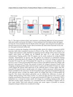
3.1 Structure of avalanche microcell
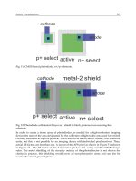
The schematic structure of the avalanche microcell of a SiPM is shown in Figure 9 and
presents a configuration n
+
-p-π-p
+
, where π represents very slight p-type doping.
Fig. 9. Schematic structure of avalanche microcell of SiPM.
Photodiodes - World Activities in 2011
192
The n
+
side is thin and is the one which receives light through a window. A thickness of
about 1µm of depletion region between the thin n
+
(thickness = 0.1–1.5 µm) and p layers is
created thanks to the reverse electric field. There are three p-type layers of different doping
levels next to the n
+
layer to suitably modify the field distribution across the structure. The
first is a thin p-type layer, the second is a thick lightly p-type doped (almost intrinsic) π-
layer of ≈300 µm, and the third is a heavily doped p
+
layer ≈ 3µm thick. On the surface of the
avalanche microstructure a thin metal layer is placed (≈ 0.01 µm) with an antireflection
coating. Above the n
+
region, a resistive SiO
2
layer (thickness ≈0.15 µm, ρ ≈ 10
5
-10
7
Ωcm)
limits the Geiger breakdown propagation by a local reduction of the electric field.
The electric field is at a maximum at the n
+
p junction, then decreases slowly through the p-
layer. The field vanishes at the end of the narrow depletion layer in the p
+
side, as shown in
Figure 10 [33].
Fig. 10. Configuration of the electric field. The high-field region (E≈5×10⁵ V/cm) is built up
in the highly doped n+p.
The absorption of photons of λ≈400 nm takes place mainly in the π-layer. The nearly
uniform field here separates the electron–hole pairs and drifts them at velocities near
saturation towards the n
+
and p
+
sides, respectively. When the drifting electrons reach the p-
layer it may be accelerated by the high fields to sufficiently large kinetic energies to further
cause impact ionization and release more electron-hole pairs which leads to an avalanche of
impact ionization processes. Thus, from a single electron entering the p-layer, one can
generate a large number of electron-hole pairs all of which contribute to the observed
photocurrent. In this mode, any electron event in the sensitive area will produce a very large
current flow with amplification gain of up to 10
6
.
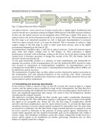
3.2 Operation principle of a SiPM
As mentioned in the previous paragraph the SiPM is a matrix of GM-APDs connected in
parallel. A schematic representation of the device is shown in Figure 11. The connection
between the cells is made on one side by the low-resistivity substrate and on the other side
by a metal layer. The diodes (labelled as D) are asymmetric p–n junctions. Each GM-APD
has in series a quenching resistor (R
Q
) which is needed to stop the avalanche current and,
then, to restore the initial bias condition enabling the detection of a new incoming photon. A
reverse bias voltage (V
bias
) is applied to each junction through the common substrate
electrode to deplete the n
+
–p junctions.
Silicon Photo Multipliers Detectors Operating in
Geiger Regime: an Unlimited Device for Future Applications
193
Fig. 11. Equivalent electric scheme of the SiPM
4. Test of static characteristics
The breakdown voltage (V
break
) and the R
Q
values are determined thanks to the reverse and
forward current–voltage (I–V) characteristics curves.
The MPPCs used for this work have an active surface of 1 X 1 mm
2
, divided into 1,600 pixels
of 25μm x 25μm (Figure 12, Figure 13 and Figure 14), and of 3 X 3 mm
2
, divided in 14,400
pixels of 25μm x 25μm (Figure 15 and Figure 16 : from Hamamatsu data sheet) [34].
Fig. 12. Aspect and external dimensions of the MPPC 1 X 1 mm
2
under characterization.
Photodiodes - World Activities in 2011
194
Fig. 13. Operating parameters of the MPPC 1 X 1 mm
2
as delivered by the supplier.
Fig. 14. a) A Photograph of the MPPC S10362-11-025U by Hamamatsu. b) Structure of a
MPPC pixel.
Fig. 15. Aspect and external dimensions of the MPPC 3 X 3 mm
2
under characterization.
Silicon Photo Multipliers Detectors Operating in
Geiger Regime: an Unlimited Device for Future Applications
195
Fig. 16. Operating parameters of the MPPC 3 X 3 mm2 as delivered by the supplier.
A V
break
of 70.1 V has been obtained for S10362-11-025U 1 X 1 mm
2
SiPM, thus demonstrating a
good uniformity of the V
break
for different SiPM’s. The value of the quenching resistor
extracted from the forward characteristics is of ~145 Ω, giving for a single micro-cell a value of
230 kΩ (see Figure 17). In fact the global resistance measured is related as:
R
SiPM
= R
micro_cell
/N
micro_cell
where N
micro-cell
= 1,600 for the S10362-11-025U model of 1 X 1 mm
2
SiPM and N
micro-cell
=
14,400 for the S10931-025P model of 3 X 3 mm
2
SiPM.
Fig. 17. Forward characteristics of S10362-11-025U SIPM (1 x 1 mm
2
).
A similar measurement on the 3x3 mm
2
SiPM led to a global resistance of 26 Ω, giving a
single pixel quenching resistance of ~ 380 kΩ.
In the Figure 18, the reverse biased portion of the I-V curve is shown, for the 3x3 mm
2
SiPM.
This side of the curve is used to extrapolate from the fit, the most convenient bias voltage to
apply to the device.
5. Dynamic characteristic and basic performances
A circuit model, which emulates the evolution of the signal of a GM-APD was developed in
the 1960s to describe the behaviour of micro-plasma instability in silicon [35, 36]. According
to this model, the pre-breakdown state can be represented as a capacitance (junction
capacitance, C
D
) in series with the quenching resistor.