Superconductivity Theory and Applications Part 12 docx
Bạn đang xem bản rút gọn của tài liệu. Xem và tải ngay bản đầy đủ của tài liệu tại đây (1.45 MB, 25 trang )
4 Will-be-set-by-IN-TECH
An inhomogeneous applied field and imperfect gradiometer balance result in a crosstalk of
the field to the SQUID and reduce a dynamic range of the CRSM. In SSSM a compensation
coil wound on an upper part of the solenoid and supplied with an adjustable current derived
from the solenoid supply current minimizes crosstalk. A careful design and construction
keeps down deformation of the field affected by a proximity of magnetic or superconducting
materials (solder) and frequency dependent eddy currents in metallic (nonsuperconducting)
parts.
The magnetic moment of the sample is
m
=
1
2
V
(
r ×j
)
d
3
r. (2)
A vector potential of the induced or spontaneous magnetic moment m of the sample is
A
= μ
m
×r
r
3
. (3)
The magnetic flux in the pickup coil is
Φ
=
Γ
A ·dl, (4)
where Γ is the coil circumference. The SQUID indicates difference in the flux in an upper and
lower coil, ΔΦ
= Φ
upper
− Φ
lower
, and thus the SQUID output voltage is proportional to a
projection of the measured magnetic moment on a gradiometer axis, m
(t) ∝ΔΦ(t).
Since the detection system is superconducting, the output voltage m
(t) is proportional to the
magnetic moment of the sample and not to a rate of change of the magnetic moment like in
case of induction magnetometers (ac susceptometer (ACS) or vibrating sample magnetometer
(VSM)).
Both the SSSM and HSSM use bulk Nb SQUID of the Zimmerman type operating at the rf
frequency of about 40 MHz. The Josephson junction is a point contact type in the SSSM and
thin film bridge in the HSSM. Both SQUIDs have an equivalent input flux noise density of the
order of 10
−4
Φ
0
Hz
−1/2
in a white noise region (> 1 Hz) and range ±500 Φ
0
limited by a slew
rate 10
4
Φ
0
/s.
3
A shielding of an external dc and time varying electromagnetic field originating from an earth
magnetic field and man-made sources is necessary to utilize the extraordinary sensitivity of
the SQUIDs. The shielding is ensured by a soft magnetic materials (the cryostat is placed
inside the shielding) and superconducting shielding (Tsoy et al., 2000).
2.3 Sample mounting and temperature reading and control
In SSSM a sample is glued on a bottom surface of a cylindrical sapphire holder using a varnish
or grease. A sample temperature sensor, the Si or GaAlAs diode
4
, is mounted on the upper
surface. The sapphire holder is connected to a (nonmagnetic, nonconducting) polyethylene
straw that extends a thin wall stainless tube suspended in an anticryostat. Another Si diode
3
iMAG 303 SQUID: The equivalent input noise for the standard LTS SQUID system is less than 10
−5
Φ
0
Hz
−1/2
, from 1 Hz to 50 kHz in the ±500 Φ
0
range. The response is flat from DC to the 3 dB points,
slow slew mode 500 Hz (- 3 dB), normal slew mode 50 kHz (- 3 dB). The input inductance of the LTS
SQUID is 1.8
×10
−6
H.
4
Lake Shore or CryoCon
264
Superconductivity – Theory and Applications
Critical State Analysis Using Continuous Reading SQUID Magnetometer 5
temperature sensor measures temperature of the anticryostat to facilitate better closed-loop
temperature control. Two section resistance wire (constantan) heater is wound around the top
and bottom part of the anticryostat to ensure uniform warming. Heat is removed from the
sample by a
4
He gas at atmospheric pressure.
In HSSM the sample is mounted on the upper surface of the sapphire holder. The holder is
embedded in a copper block whose temperature is measured using the Si diode sensor. The
block is heated using a resistance wire heater and suspended on a low thermal conductivity
fibreglass support which removes heat to liquid
4
He bath. The sample is in vacuum.
In both magnetometers, a temperature controller
5
connected to the computer regulates
temperature with relative stability of 10 ppm and 1 ppm in SSSM and HSSM, respectively,
and controls cooling or warming with rate from 1 mK/min to 10 K/min.
2.4 Measurement modes
The magnetometers are designed for measurements of: i) temperature dependence of a
response to fixed AC and DC applied magnetic field (temperature dependence of the
susceptibility); ii) response to field sweep at fixed temperature and AC field (magnetization
loops and AC susceptibility); iii) relaxation of a DC magnetic moment (after applied field
pulse or step) as a function of time or temperature; iv) frequency dependence at a fixed DC
field and temperature. Additional measurement modes require only a software change.
2.5 Data acquisition
The dynamic range of the SQUID is extraordinary, the range of ±500 Φ
0
and spectral flux
noise density of 10
−4
Φ
0
Hz
−1/2
represent output voltage range ±10 V and voltage noise
density 10 μVHz
−1/2
, a range of 7 orders (140 dB).
6
The frequency response is flat both in a
frequency and phase. In slow slew mode the -3 dB point is 100 Hz. The SQUID output signal
m
(t) falls into an audio range and thus may be easily digitized in "CD" quality as well as the
signal of the applied field H
(t), recorded on a hard disk, and digitally processed in real time.
7
Processed data file includes temperature readings.
2.6 AC susceptibility measurement (calculation)
Let the time varying applied AC magnetic field is
H
(
t
)
=
H
ac
cos
(
2π f
0
t
)
=
H
ac
Re exp
(
i2π f
0
t
)
, (5)
where H
ac
is the amplitude and f
0
is the frequency of the applied field. The complex AC
susceptibility of the sample is
χ
n
=
M
(
nf
0
)
H
ac
V
, (6)
5
CryoCon model 34
6
This applies to rf-SQUIDs. The flux noise density in DC SQUIDs is lower, 10
−6
Φ
0
Hz
−1/2
,
corresponding voltage noise density 0.1 μVHz
−1/2
, and dynamic range of 9 orders (180 dB).
7
We use the National Instruments PC cards model PCI-4451 with Σ − Δ digital to analog and analog
to digital converters for a digital signal generation and acquisition (two input channels with 16 bit
resolution, frequency range from 0 (true DC) to 95 kHz, and sampling rate up to 204.8 kS/s).
265
Critical State Analysis Using Continuous Reading SQUID Magnetometer
6 Will-be-set-by-IN-TECH
where n denotes harmonics and M(nf
0
) are the Fourier components of the magnetic moment
m
(t). Higher harmonics of the complex susceptibility appear in the case of a nonlinear
response to the applied field. Usually the susceptibility is normalized to a volume V (or mass)
of the sample. Using the susceptibility, the magnetization loops are
M
(
H
(
t
))
=
∑
n
χ
n
H
ac
exp
(
ni2π f
0
t
)
, (7)
A common way to measure the AC susceptibility is to detect a signal of the magnetic moment
using a phase sensitive lock-in amplifier, preferably a two phase instrument indicating both
real and imaginary part of the AC susceptibility, and drive the AC field using a signal
generator. The conventional analog lock-in amplifier multiplies the input signal m
(t) by a
square wave r
(t) derived from a reference signal H(t) and integrates the product. The DC
output are in-phase and out-of-phase components
Re
M( f
0
)=
4
πτ
t
t
−τ
∞
∑
n=1
1
n
sin
(n
π
2
) cos
n2π f
0
t
m
(t
)dt
, (8)
Im
M( f
0
)=
4
πτ
t
t
−τ
∞
∑
n=1
1
n
sin
n2π f
0
t
m
(t
)dt
, (9)
where n is odd and τ is the averaging time constant. Since the reference signal r
(t) is a square
wave, the DC output is proportional not only to the Fourier component of the first harmonic
but also to 1/3 of third, 1/5 of fifth, etc. Evidently, this way of signal processing is not suitable
for the measurement of a nonlinear response. One can apply input filters that sufficiently
suppress third and higher odd harmonics, but remain unaffected the fundamental frequency.
However, suitable tunable filters are complex and expensive.
In the digital signal processor (DSP) lock-in amplifiers the signal is filtered with a simple
anti-aliasing filter and digitized by over-sampling ADC with subsequent digital filtering. The
DSP chip then synthesizes digital reference sine (and cosine) wave at the reference frequency
nf
0
and multiplies the signal by this reference. After multiplication, stages of digital low-pass
filtering are applied to average over the signal period. The DSP lock-in amplifier generates
the true rms values of the complex Fourier components of
M( f
0
) or nth harmonic M(nf
0
):
M
(
nf
0
)
=
1
NΔt
N−1
∑
k=0
m
(
t
k
)
exp
(
ni2π f
0
t
k
)
, (10)
where Δt
= t
k
− t
k−1
is the sampling interval and NΔt is averaging time. However,
commercial DSP lock-in amplifiers provide only components at single frequency. Hence,
unless successive measurements of the harmonics are done, one needs an extra instrument
for the each additional harmonic.
With computational power of today’s processors in personal computers (PC) and data
generation/acquisition hardware the problem as a whole may be solved much more
effectively. The single PC card, with essentially the same ADC as are used in the DSP lock-in
amplifier, substitutes for the generator and lock-in amplifiers. Since the DACs generating
the applied field and ADCs sampling m
(t) and H(t) use the same clock, synchronization is
guaranteed. In reality, an approach using a direct digital signal generation, acquisition, and
processing is more cost effective and less time consuming.
266
Superconductivity – Theory and Applications
Critical State Analysis Using Continuous Reading SQUID Magnetometer 7
The nth harmonic of the AC susceptibility is given by generalized Eq. 6,
χ
n
=
M(
nf
0
)
H
ac
exp(niϕ)
, (11)
where complex H
ac
exp(niϕ) ≡|H( f
0
)|exp(ni arg H( f
0
)) takes into account a phase of the
Fourier component of the applied field
H( f
0
), i.e. a time shift between a Fourier transformed
data segment and cosine field. The
M( f ) and H( f ) spectra are computed using a discrete fast
Fourier transform (FFT) of real data arrays m
(t
k
) and H( t
k
).
M
l
≡
N−1
∑
k=0
m(t
k
) exp
(
i2πkl /N
)
, (12)
(the same holds for H
(t) ⇔H( f )), where N is the transform length (Press et al., 1992). Spectra
of the complex amplitudes
M( f ) and H( f ) are calculated for frequencies lΔ f , M
l
≡M(lΔ f ).
With an applied FFT algorithm N must be a power of 2, FFT is computed in N log N
operations, and Δ f
= f
s
/N, where f
s
= 1/Δt is the sampling frequency.
8
Unlike the DSP
lock-in amplifiers, where another instrument performing N operations to process NΔt long
record is need for each measured harmonic, here the whole frequency spectrum from DC to
f /2 is computed with only N log N operations using the single instrument. Computation time
takes few ms.
Strictly speaking, the measurement of temperature dependence of the susceptibility represents
a continuous measurement of magnetization loops at slowly varying temperature. Since
the input signals are recorded as well as temperature readings, various time domain and
frequency domain filters may be applied thereupon. The magnetization loops may be
processed using different time windows (for example to remove a linear trend in m
(t)) or
different averaging times.
3. Critical state in type II superconductors
3.1 Vortex matter
Type II superconductors, ie. those with λ/ξ > 2
−1/2
, where λ is the flux penetration length
and ξ is the coherence length of a superconducting order parameter, remain superconducting
even in a high magnetic field due to lowering of their energy by creating walls between normal
and superconducting regions. Consequently, flux lines (vortices) with a normal core of a
radius of
≈ ξ, where the order parameter vanishes, and persistent current circulating around
the core and decaying away from the vortex core at distances comparable with λ are created
at sample edges and penetrate into an interior of the superconductor. The vortex is a linear (in
three dimensions) object which is characterized by a quantized circulation of the phase of the
order parameter around its axis and carries a single quantum of the magnetic flux Φ
0
= h/2e.
The superconductor penetrated with the flux lines is called to be in a mixed state. A repulsive
interaction between the flux lines eventually forms flux line bundles and consecutively a flux
8
Let us take N = 2
14
(16 K samples), easy for real time processing on a common PC. With f
s
= 6.4 kS/s
the Δf
= 0.390625 Hz. A right choice for the AC field frequency f
0
is an integer multiple of Δ f . For
example, with f
0
= 4Δ f = 1.5625 Hz, one period of the AC field is represented by 4 K samples. In this
case the 16 K FFT means averaging over 4 periods (2.56 s) of the AC field. If the 16 K data are shifted
by 4 K and a void part is replaced with samples of the latest read period, the spectra are averaged over
2.56 s and updated in 0.64 s interval. The index of the nth harmonics amplitude is l
= n4.
267
Critical State Analysis Using Continuous Reading SQUID Magnetometer
8 Will-be-set-by-IN-TECH
line lattice. In increasing applied field the flux lines enter into the superconductor when the
magnetic field exceeds the lower critical field H
c1
≈ Φ
0
/μ
0
λ
2
. Type II superconductors
experience a second-order phase transition into a normal state at the upper critical field
H
c2
≈ Φ
0
/μ
0
ξ
2
. In type I superconductors this transition is a first-order in a nonzero field.
3.2 Pinning and surface barrier
In a real type II superconductor there are always crystal lattice distortions, voids, interstitials,
and impurities with reduced superconducting properties. The superconducting order
parameter is either reduced or suppressed completely, just as within a vortex core. That
implies that such defects are energetically favorable places for vortices to reside and the
vortices will be pinned in the potential of these so-called pinning centers. The efficiency of
such a pinning center is at its maximum if its size is of the order of the coherence length ξ.If
there is almost no pinning, flux flow occurs (Bardeen, 1965). On the other hand, when there is
finite pinning, flux creep of a vortex bundles takes place (Anderson, 1962; 1964). The bundle
size is determined by the competition between pinning and the elastic properties of the vortex
lattice.
An edge or surface barrier may oppose a flux entry into the sample (Beek et al., 1996). A
surface barrier arises as a result of the repulsive force between vortices and the surface
shielding current. The first example is Bean-Livingston barrier, which is a feature of flat
type II superconductor surfaces in general and is related to a deformation of the vortex at the
surface (mirror vortex). The second example is the edge-shape barrier, which is a geometric
effect related to the distribution of the Meissner shielding current density in non-ellipsoidal
samples.
When an increasing magnetic field is initially applied, flux cannot overcome the barrier, and
M
= −H. At the field of the first flux penetration H
p
, the magnetic pressure is sufficiently high
to overcome the barrier. If there is no pinning, vortices will now distribute themselves through
the sample in such a way that the bulk current is zero and vortex density is homogeneous.
3.3 Flux line dynamics
When the superconductor is carrying a bulk transport or shielding current density j the
flux lines experience a volume density of the driving Lorentz force f
L
= j × B, where B
is the flux density inside the flux line. When the Lorentz force acting on the flux lines is
exactly balanced by the pinning force density, i.e. F
L
= F
p
, the current density is called the
depinning current density, j
c
. Under this force the flux lines may move through the crystal
lattice and dissipate energy. In this case the electrical losses are no longer zero. In an ideal
(homogeneous) type II superconductor there is nothing to hinder the motion of flux lines and
the flux lines distribution is homogeneous. The flux lines can move freely, which is equivalent
to a vanishing critical depinning current density j
c
. On the other hand, the non-dissipative
macroscopic currents are the result of the spatial gradients in the density of flux lines or due
to their curvature. This is possible only due to the existence of pinning centers, which can
compensate the Lorentz force.
The moving flux lines dissipate energy by two effects which give approximately equal
contributions: (a) eddy currents that surround each moving flux line and have to pass through
the vortex core, which in the model of Bardeen and Stephen is approximated by a normal
conducting cylinder (normal currents flowing through the vortex core) (Bardeen, 1962); (b)
268
Superconductivity – Theory and Applications
Critical State Analysis Using Continuous Reading SQUID Magnetometer 9
Tinkham’s mechanism of a retarded recovery of the order parameter at places where the
vortex core has passed (Tinkham, 1996).
In general, the current density in type II superconductors can have three different origins: (a)
Surface currents within the penetration depth λ. In the Meissner state the current passing
through a thick superconductor is restricted to a thin surface layer where the magnetic
field can penetrate. Otherwise the magnetic field due to the current would exist inside the
superconductor; (b) A gradient of the flux-line density; (c) A curvature of the flux lines.
A flux line motion is discouraged (inhibited) by pinning of individual flux lines, their bundles
or lattice. In cases of flux flow and flux creep, the vortices are considered to move in an
elastic bundle. With discovery of HTS, however, more complex forms of vortex motion are
considered. When the driving force is small, the vortices move in a plastic manner - plastic
flow where there are channels in which vortices move with a finite velocity, whereas in other
channels the vortices remain pinned (Jensen, 1988). Thus, between moving channels and static
channels there are dislocations in the flux lattice. With further increasing driving current,
vortices tend to re-order. Through dynamic melting, a stationary flux lattice changes into a
moving flux lattice via the plastic flow (Koshelev & Vinokur, 1994).
If pinning is efficient the critical depinning current density j
c
becomes high and the material
is interesting for applications. The properties of the flux line lattice and the pinning properties
are important for applications; on the other hand they are complex and interesting topics of
condensed-matter physics and materials science.
3.4 Equation of motion of vector potential
In general, computation of magnetization loops represents a full treatment of a nonlinear 3D
problem described by a partial differential equation for a vector potential
∂A
∂t
= D∇
2
A, (13)
where D is the diffusivity. Due to an axial symmetry or for a long sample in a parallel field,
the problem may reduce to 2D and the current density j, vector potential A, and electric field
E are parallel to each other and have only a y or φ component (applied field is parallel to z
axis) (Brandt, 1998). The magnetization loops are obtained solving Eq. 13 using specialized
software packages or directly by the time integration of the nonlocal and nonlinear diffusion
equation of motion for the azimuthal current density. A long cylinder or slab in parallel field
or thin circular disk and strip in an axial field are 1D problems. The flux density and electric
field are B
= ∇×A and E = −∂A/∂t, respectively.
In the normal (nonsuperconducting) state with an ohmic conductivity σ is D
= 1/μ
0
σ =
m/μ
0
ne
2
τ. In Meissner state the diffusivity is the pure imaginary D = iωm/μ
0
n
s
e
2
with a
linear frequency dependence, where n
s
is the superconducting condensate density.
In an inhomogeneous type II superconductor with flux pinning the electric field is given by
nonlinear local and isotropic resistivity ρ
(j). A material law E(j) reflects a flux line pinning.
In case of a strong pinning E
(j) is zero up to the critical depinning density j
c
at which electric
field raises sharply. A power law voltage current relation
E
(j)=E
c
|j/j
c
|
n
j/j = ρ
c
|j/j
c
|
n−1
j, (14)
269
Critical State Analysis Using Continuous Reading SQUID Magnetometer
10 Will-be-set-by-IN-TECH
where j = |j|, is observed in numerous experiments (Brandt, 1996). From the theories on
(collective) creep, flux penetration, vortex glass picture, and AC susceptibility one obtains the
useful general interpolation formula
U
(J)=U
0
(j
c
/j)
α
−1
α
. (15)
Here U
(j) is a current-dependent activation energy for depinning which vanishes at the
critical current density j
c
, and α is a small positive exponent. In the limit α → 0 one has a
logarithmic dependence of the activation energy U
(j)=U
0
ln(j
c
/j), which inserted into an
Arrhenius law yields
E
(j)=E
c
exp
−
U
(
j
)
k
B
T
= E
c
j
j
c
U
0
/k
B
T
. (16)
When we compare Eq. 16 with Eq. 14 the exponent is n
= U
0
/k
B
T. For α = −1 the Eq.
15 coincides with the result of the Kim-Anderson model, E
(j)=E
c
exp[(U
0
/k
B
T)(1 − j/j
c
)],
(Blatter et al., 1994). For α
= 1 one gets E(j)=E
c
exp[(U
0
/k
B
T)( j
c
/j − 1)].
In general, the E
c
and activation energy U in Eq. 16 depend on the local induction B(r) and
thus also α
(B, T) and j
c
(B, T) depend on B.
With E
= −∂A/∂t and Eq. 14 one obtains for the diffusivity in Eq. 13
D
(j, j
c
, U
0
, T)=
1
μ
0
∂E
∂j
=
1
μ
0
E
c
j
c
j
j
c
U
0
/k
B
T−1
=
ρ
c
μ
0
j
j
c
U
0
/k
B
T−1
. (17)
Power-law electric field versus current density (Eq. 14) induces:
i) An Ohmic conductor behavior with a constant resistivity ρ
= E/j for U
0
/k
B
T = 1. This
applies also to superconductors in the regime of a linear flux flow or thermally activated
flux flow (TAFF) at low frequencies with flux-flow resistivity ρ
f
= ρ
n
B/μ
0
H
c2
, known as
the Bardeen-Stephen model. The diffusivity D is large and vector potential profiles are time
dependent. The magnetization loops have a strong frequency dependence, as well as the
susceptibility, and the AC susceptibility has only fundamental component independent on
the AC field amplitude (Gömöry, 1997).
ii) Flux creep behavior for 1
U
0
/k
B
T < ∞. The magnetization loops have a weak frequency
dependence, as well as the AC susceptibility which has higher harmonics and is dependent
on the AC field amplitude.
iii) Hard superconductors with strong pinning for U
0
/k
B
T → ∞. In this case the flux
dynamics is quasistatic, described by a Bean model of the critical state with D
= 0 for |j| < j
c
and D → ∞ for |j| = j
c
. The magnetization loops are frequency independent, as well as the AC
susceptibility which has higher harmonics and strongly depends on the AC field amplitude.
A general solution of Eq. 13 represents time dependent vector potential profiles which
dynamics covers a viscous flow, diffusion (creep), and quasistatic (sand pile like) behavior.
The resistivity generated by the flux creep is Ohmic in the low-driving force limit.
3.5 Analytically solvable models
3.5.1 Normal state with ohmic conductivity and flux flow state
In normal state with an ohmic conductivity σ = ne
2
τ/m the diffusion constant is D =
1/μ
0
σ = ωδ
2
, where ω is the angular frequency of the applied AC field and δ =(2μ
0
ωσ)
−1/2
270
Superconductivity – Theory and Applications
Critical State Analysis Using Continuous Reading SQUID Magnetometer 11
is the normal skin depth. In this case the analytical solutions to Eq. 13 are known for an
infinitely long cylinder and slab in a parallel field, cylinder in a perpendicular field, and sphere
(Brandt, 1998; Khoder & Couach, 1991; Lifshitz et al., 1984).
With an increasing ratio δ/R or δ/d, where and R is the radius of the cylinder or sphere and 2d
id the slab thickness, a sample changes from a diamagnetic (but lossy) at δ
R, to absorptive
at δ
≈ R, and to transparent for applied field at δ R . The magnetization loops M(H)
are ellipses which major axis lies on H axis of H − M diagram for transparent medium and
gradually turns to
−π/4 direction for diamagnetic medium. The susceptibility as a function
of
(δ/R)
2
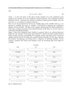
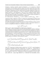
is shown in Fig. 2.
In a limit of low frequencies when the skin depth δ
R, d and the sample is transparent for
AC field the first terms in series expansion of the susceptibility are (up to a shape dependent
multiplication factor)
Reχ
≈−
R
2
μωσ
2
(18)
Imχ
≈
R
2
μωσ
, (19)
and Reχ
Imχ. A measurement of χ yields contactless estimation of the electrical
conductivity σ.
In a linear or thermally activated flux flow state as the applied field approaches the upper
critical field H
c2
, the flux density in the superconductor B → μ
0
H
c2
and the flux flow
resistivity ρ
f
smoothly transforms to ρ
n
= 1/σ
ρ
f
ρ
n
≈
B
μ
0
H
c2
(20)
as the phase transition between a mixed state and normal state is of second order (Bardeen
Stephen model) (Bardeen, 1965). Flux flow resistivity may be estimated using Eq. 19.
3.5.2 Meissner state
At initial magnetization the superconductor is in Meissner state in field lower that H
c1
.In
this case the diffusivity is pure imaginary D
= iωλ
2
, where the flux penetration length is
λ
=(μ
0
n
s
e
2
/m)
−1/2
. The susceptibility of an infinitely long cylinder and slab in a parallel
field, cylinder in a perpendicular field, and sphere is obtained like for normal state but
replacing
(1 + i)/δ with i/λ (Brandt, 1998; Khoder & Couach, 1991; Lifshitz et al., 1984). The
susceptibility as a function of
(λ/R)
2
is shown in Fig. 2.
In a weak field, low temperature part of the susceptibility (T/T
c
< 0.5) is proportional to the
flux penetration length
Reχ
(T)=−1 + aλ(T)/R. (21)
A measurement of temperature dependence λ
(T) allows us to distinguish different
pairing symmetries. While in conventional superconductors with an isotropic gap
the quasiparticle excitations rise with increasing temperature as exp
(−Δ/k
B
T),in
nonconventional superconductors, for example HTS, a temperature dependence is power-law.
As far as we know, it fails to fit experimental χ
(T) at T → T
c
even for well known λ(T),at
low temperatures.
271
Critical State Analysis Using Continuous Reading SQUID Magnetometer
12 Will-be-set-by-IN-TECH
-1.2
-1
-0.8
-0.6
-0.4
-0.2
0
0.2
0.4
0.6
1E-06 1E-05 0.0001 0.001 0.01 0.1 1 10 100 1000
(
d/
R)
2
Susceptibility
ReX sphere
ImX sphere
ReX slab
ImX slab
SC sphere
SC slab
SC cylinder
Fig. 2. The dependence of the complex AC susceptibility of a sphere and slab in a normal
(ohmic) state in a parallel field on
(δ/R)
2
∝ ρ
n
and of the sphere, slab and cylinder in
Meissner state on
(λ/R)
2
∝ 1/n
s
. In an ohmic state an absorption peak appears on Imχ, the
height of which is characteristic of sample shape.
3.5.3 Bean critical state
The Bean model of the critical state is the case of a strong pinning when the flux density
variation is quasi-static (frequency independent) in a slowly varying applied magnetic field
and the flux density profile changes only when induced shielding current density reaches the
critical depinning current density j
= ±j
c
. An electric field is induced when the flux density
changes. In a slab the flux density profile is linear
|∂B
z
(x)/∂x| = μ
0
j
c
in flux penetrated
regions and
|B| = 0 in untouched regions. The model assumes lower critical field H
c1
→ 0,
surface barrier H
barrier
→ 0, and field independent critical depinning current density j
c
, i.e.
j
c
(B) is constant (Bean, 1964).
Analytical solutions for magnetization loops are known for an infinitely long slab or cylinder
in a parallel field (Goldfarb, 1991) and thin disk (Clem & Sanchez, 1994; Mikheenko &
Kuzovlev, 1993) or strip (Brandt, 1993) in a perpendicular field. In these cases the 3D partial
differential equation (PDE) Eq. 13 reduces to a time independent 2D PDE due to sample shape
symmetry.
The model to the disks was work out by Clem and Sanches who improved and corrected
former model worked out by Mikheenko and Kuzovlev (Clem & Sanchez, 1994). The model
is restricted to slow, quasistatic flux changes for which the magnitude of the electric field E
induced by the moving magnetic flux is small in comparison with ρ
f
j
c
, where ρ
f
is the flux
flow resistivity. Under these conditions, the magnitude of the induced current density is close
to the critical depinning current density. The validity of the model is restricted for d
R,
d
≥ λ or if d < λ, that Λ = 2λ
2
/d R, where λ is the flux penetration length and Λ is the
2D screening length.
In the case of the infinitely long (or sufficiently long) sample (slab or cylinder) in parallel
applied field the shielding current density is at a surface parallel with applied field,
μ
0
j
φ
= −∂B
z
/∂r (22)
while in case of the sufficiently thin sample (disk or strip) in perpendicular applied field
272
Superconductivity – Theory and Applications
Critical State Analysis Using Continuous Reading SQUID Magnetometer 13
μ
0
j
φ
= ∂B
r
/∂z, (23)
the shielding current appears simultaneously everywhere over the sample cross-section upon
application of the field, and decreases everywhere simultaneously after a decrease of the
field (Beek et al., 1996). The complete magnetic hysteresis loop can be obtained from the
first magnetization curve, which is almost the same for the above cases. The hysteresis loop
develops from the thin lens-shaped to parallelogram as the H
ac
is increased or j
c
decreases.
The lens shape corresponds to partial penetration of the magnetic flux while the parallelogram
occurs when the magnetization is saturated.
The component of the magnetization parallel to the applied periodically time varying field
H
(ϕ)=H
ac
sin ϕ is
M
∓
= ∓χ
0
H
ac
S
H
ac
H
d
±χ
0
(
H
ac
∓ H
)
S
H
ac
∓ H
2H
d
, (24)
where M
−
and M
+
are for decreasing and increasing applied field, respectively (Clem &
Sanchez, 1994). A characteristic field H
d
= dj
c
/2, where d is the disk thickness and j
c
is
the critical depinning current density (temperature dependent). The function S
(x) is defined
as
S
(
x
)
=
1
2x
arccos
1
cosh x
+
sinh |x|
cosh
2
x
. (25)
3.5.4 Mapping of model susceptibility to experimental susceptibility
The model AC susceptibility is calculated for magnetization loops Eq. 24 using Eq. 11, i.e.
in the same way as the experimental susceptibility (Youssef et al., 2009). To map the model
susceptibility χ
(H
ac
/H
d
) to the experimental temperature dependent susceptibility χ(T) we
use a proportionality of the characteristic field to the critical depinning current density, H
d
=
dj
c
/2, and a fact that experimentally observed temperature dependence, j
c
(T)=j
c
(0)(1 −
T/T
c
)
n
, is power-law. Further, we need an inverse function for j
c
(T) and insert the amplitude
of the applied field. Let us take
j
c
(T)
j
c
(0)
=
H
d
(T)
H
d
(0)
=
1
−
T
T
c
m
n
. (26)
Relation between temperature T and ratio H
d
/H
ac
, i.e. experimental and model susceptibility,
is obtained using inverse function for Eq. 26 and multiplying both the numerator and
denominator, H
d
/H
d
(0),byH
ac
T
T
c
model
=
1
−
H
ac
H
d
(0)
H
d
H
ac
1/n
1/m
. (27)
We have four free parameters c
≡ H
ac
/H
d
(0), n, m, and T
c
to match the model and
experimental susceptibility
⎡
⎣
1
−
c
H
d
H
ac
1
n
1
m
, χ
H
d
H
ac
⎤
⎦
←→
T
T
c
, χ(T)
. (28)
273
Critical State Analysis Using Continuous Reading SQUID Magnetometer
14 Will-be-set-by-IN-TECH
When we find c, n, m, and T
c
, the zero temperature critical depinning current density is
j
c
(0)=2H
ac
/cd (29)
and its temperature dependence is given by Eq. 26.
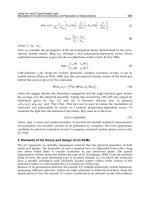
-0.06
-0.05
-0.04
-0.03
-0.02
-0.01
0
0.01
0.02
-3 -2.5 -2 -1.5 -1 -0.5 0
-(H
p
/3H
ac
)
1/3
, -(H
d
/H
ac
)
1/2
3rd harmonic of ac susceptibility
ReX(3) Cylinder
ImX(3) Cylinder
ReX(3) Disk
ImX(3) Disk
(a) The third harmonic of the AC susceptibility.
-0.015
-0.01
-0.005
0
0.005
-3 -2.5 -2 -1.5 -1 -0.5 0
-(H
p
/3H
ac
)
1/3
, -(H
d
/H
ac
)
1/2
5th harmonic of ac susceptibility
ReX(5) Cylinder
ImX(5) Cylinder
ReX(5) Disk
ImX(5) Disk
(b) The fifth harmonic of the AC susceptibility.
Fig. 3. Differences in the harmonics of AC susceptibility for models of cylinders and disks.
The susceptibility is plotted versus "model temperature" given by Eq. 27 (Youssef et al.,
2009). Here H
p
is the characteristic field for a cylinder, H
p
= Rj
c
.
3.5.5 Interpretation of complex AC susceptibility
The real part of the fundamental AC susceptibility represents a magnetic energy of the
sample stored in the diamagnetic shielding current. The imaginary part of the fundamental
susceptibility is related to losses caused by resistive response (dissipation).
In normal state or in flux flow state the AC susceptibility is a function of applied
field frequency, conductivity (resistivity), and temperature but is independent of the field
amplitude. On the other hand, in a case of strong pinning the AC susceptibility is a function
of the applied field amplitude, critical depinning current density, and temperature but is
independent of frequency. Nonlinear dependence of the sample magnetization on applied
field amplitude generates harmonics of AC susceptibility. Their behavior is characteristic for
a given sample shape. Due to a symmetry of the magnetization loops, M
(H)=−M(−H),
the coefficients of even harmonics of the AC susceptibility are zero.
4. Experimental results on critical state in type II superconductors
Recently developed second generation of the high temperature superconductor wires on the
basis of YBaCuO films and Nb films for superconductor electronics production represent
proper materials to study models to the critical state in hard superconductors.
274
Superconductivity – Theory and Applications
Critical State Analysis Using Continuous Reading SQUID Magnetometer 15
4.1 Materials
The Nb film of thickness of 250 nm was deposited by a dc magnetron sputtering in Ar gas
on 400 nm thick silicon-dioxide buffer layer which was grown by a thermal oxidation of a
silicon single crystal wafer (May, 1984). The film is polycrystalline with texture of a preferred
orientation in the (110) direction and is highly tensile. Grain size is about 100 nm. The square
samples of 5
× 5mm
2
in dimensions were cut out from the 3-inch wafer.
Second-generation high temperature superconductor wire (2G HTS wire) consists of a 50 μm
nonmagnetic nickel alloy substrate (Hastelloy), 0.2 μm of a textured MgO-based buffer stack
deposited by an assisting ion beam, 1 μm RE-Ba
2
Cu
3
O
x
superconducting layer SmYBaCuO
deposited by metallo-organic chemical vapor deposition, and 2 μm of Ag, with 40 μm total
thickness of surround copper stabilizer (20 μm each side) .
9
The sample is cut into 4 mm long
segment of 4 mm wide wire.
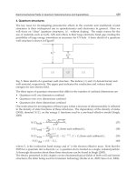
4.2 Estimation of the critical depinning current density and its temperature dependence
Since the model susceptibility is not given analytically the standard fitting procedures cannot
be applied here. A convenient way to map the model susceptibility to the experimental
one is to plot the experimental susceptibility as a function of reduced temperature T/T
c
and superimpose the model susceptibility by fitting parameters c, n, and m in Eq. 27 and
T
c
interactively (manually), see Fig. 4. The critical depinning current density estimated
using Eq. 29 is j
c
(0)=3 × 10
11
A/m
2
in the Nb film with temperature dependence
j
c
(T)=j
c
(0)[1 −(T/T
c
)]
3/2
. The critical depinning current density found in the YBCO wire
is j
c
(0)=10
12
A/m
2
with steeper temperature dependence, j
c
(T)=j
c
(0)[1 −(T/T
c
)]
2
. This
result well agrees with j
c
estimated using a four point probe contact measurements (Youssef
et al., 2009; 2010).
5. Conclusion
The thin film type II superconductors with a strong pinning allowed us to verify the complete
analytical model of a response of a thin disk in the Bean critical state to an applied time varying
magnetic field. On the other hand, the application of this model gives a contactless estimation
of the critical depinning current density and its temperature dependence.
To observe the characteristic critical state response from an YBCO sample as is shown in
Fig. 4 at lower temperatures the applied time varying field has to be of the order of 0.1
T at 77 K and of the order of 1 T at 4.2 K. Such fields may rather be generated using a
normal (nonsuperconducting) solenoid that avoids a residual field of flux lines trapped in the
superconducting solenoid winding and guaranties a linear H
(I) relation. However, dissipated
power will be large. Also, since the induced magnetic moment will be large, there is no need
for a sensitive superconducting detection system, but a detector with high linearity and flat
frequency and phase response is necessary as the maximum amplitude of 3rd harmonic is
only 6% and 5th harmonic of only 1% of the real part of the fundamental susceptibility.
The fit to the model reveals an excess of few % of the real part of the susceptibility as
temperature decreases to zero. This diamagnetic contribution is due to the temperature
9
Wire type SCS4050 SuperPower, Inc., Schenectady, NY 12304 USA. The critical current of the wire as
estimated using four probe method and 1 μV/cm criterion is from 80 to 110 A at 77 K (97 A for our
piece of wire).
275
Critical State Analysis Using Continuous Reading SQUID Magnetometer
16 Will-be-set-by-IN-TECH
-1.0
-0.8
-0.6
-0.4
-0.2
0.0
0.2
0.980 0.985 0.990 0.995 1.000
Reduced temperature (T /T
c
)
Fundamental ac susceptibility
ReX(1) YBCO
ImX(1) YBCO
ReX(1) Model YBCO
ImX(1) Model YBCO
ReX(1) Nb
ImX(1) Nb
ReX(1) Model Nb
ImX(1) Model Nb
(a) The fundamental AC susceptibility.
-0.06
-0.05
-0.04
-0.03
-0.02
-0.01
0.00
0.01
0.02
0.990 0.992 0.994 0.996 0.998 1.000 1.002
Reduced temperature (T /T
c
)
3rd harmonic of ac susceptibility
ReX(3) YBCO
ImX(3) YBCO
ReX(3) Model YBCO
ImX(3) Model YBCO
ReX(3) Nb
ImX(3) Nb
ReX(3) Model Nb
ImX(3) Model Nb
(b) The third harmonic of the AC susceptibility.
Fig. 4. Temperature dependence of the AC susceptibility of Nb and YBCO films in
perpendicular field μ
0
H
ac
= 10 μT and f = 1.5625 Hz (Youssef et al., 2010).
dependent flux penetration length λ
(T) which depends exponentially on temperature in
conventional superconductors (Nb) and obeys a power-law in unconventional ones (YBCO).
As was shown by Brandt, the normalized magnetization curves for hard (Bean)
superconductors obtained by a numerical treatment differ very little for similar geometries
(Brandt, 1996): between strips and circular disks the relative difference is
< 0.011, between
thin circular and quadratic disks the difference is
< 0.002. This makes an application of fully
analytical models for contactless estimation of the critical depinning current density and its
temperature dependence favorable.
6. Acknowledgements
The authors are grateful to SuperPower, Inc. for providing us with 2G HTS YBCO wire, and
to F. Soukup and R. Tichy for technical assistance. This work was supported by Institutional
Research Plan AVOZ10100520, Research Project MSM 0021620834 (Ministry of Education,
Youth and Sports of the Czech Republic), the Czech Science Foundation under contract No.
202/08/0722, (Javorsky SVV grant 2011-263303) and ESF program NES.
7. References
Anderson, P.W. (1962). Theory of flux creep in hard superconductors, Phys. Rev. Lett. Vol.
9:309-311.
Anderson, P.W. & Kim, Y.B. (1962). Hard Superconductivity: Theory of the Motion of
Abrikosov Flux Lines, Rev. Mod. Phys. Vol. 36:39-43.
Bardeen, J. (1962). Critical fields and currents in superconductors, Rev. Mod. Phys. Vol.
34:667-681.
Bean, C.P. (1964). Magnetization of High-Field Superconductors, Rev. Mod. Phys. Vol. 36:31-39.
276
Superconductivity – Theory and Applications
Critical State Analysis Using Continuous Reading SQUID Magnetometer 17
van der Beek, C.J., Indenbom, M.V., D’Anna, G., Benoit, W. (1996). Nonlinear AC
susceptibility, surface and bulk shielding, Physica C Vol. 258:105-120.
Blatter, G., et al. (1994) Vortices in high-temperature superconductors, Phys. Mod. Phys. Vol.
66:1125-1388.
Brandt, E.H., et al. (1993). Type-II Superconducting Strip in Perpendicular Magnetic Field,
Europhys. Lett. Vol. 22, No. 9: 735 - 740
Brandt, E.H. (1996). Superconductors of finite thickness in a perpendicular magnetic field:
Strips and slabs, Phys. Rev. B Vol. 54: 4246-4264.
Brandt, E.H. (1998). Superconductor disks and cylinders in an axial magnetic field. I.
Flux penetration and magnetization curves, Phys. Rev. B Vol. 58: 6506-6522;
Superconductor disks and cylinders in an axial magnetic field: II. Nonlinear and
linear ac susceptibilities, Phys. Rev. B Vol. 58: 6523-6533
Chen, D X., et al. (2007). Field dependent alternating current susceptibility of
metalorganically deposited YBa2Cu3O7-d films, J. Appl. Phys. 101: 073905
Clem, J.R. & Sanchez, A. (1994). Hysteretic ac losses and susceptibility of thin superconducting
disks, Phys. Rev. B Vol. 50: 9355-9362.
deGennes, P. G. (1966), In: Superconductivity of Metals and alloys (Benjamin, New York, 1966).
Goldfarb, R.B., Lelenthal, M., Thompson, C.A., Alternating-field susceptometry and magnetic
susceptibility of superconductors, In: Magnetic Susceptibility of Superconductors and
Other Spin Systems, edited by R. A. Hein (Plenum Press 1991), p. 49.
Gömöry, F. (1997). Characterization of high-temperature superconductors by AC
susceptibility measurements, Supercond. Sci. Technol. Vol. 10: 523-542.
Koshelev A.E., Vinokur V.M. (1994), Dynamic meltig of the vortex lattice, Phys. Rev. Lett. Vol.
73: 3580-3583.
Khoder, A.F. and Couach, M. (1991). Early theories of χ
and χ
of superconductors; the
controversial aspects, In: Magnetic Susceptibility of Superconductors and other Spin
Systems, New York and London: Plenum Press. p 213-228.
Lifshitz, E.M. et al. (1984) In: Electrodynamics of Continuous Media, Vol. 8 (Course of Theoretical
Physics), Ed. Butterworth-Heinemann.
May T. (1984), Ph.D. Thesis, Institute for Physical High Technology, Jena, Germany 1999.
Mikheenko P. N. & Kuzovlev Yu. E. (1993), Inductance measurements of HTSC films with high
critical currents, Physica C Vol. 204:229-236.
Press, W.H., et al. (1992). In: Numerical Recepies in C, Cambridge University Press, ISBN 0 521
43720 2, Cambridge. p 496 - 536.
Pearl, J. (1964). Current distribution in superconducting films carrying quantized fluxoids,
Appl. Phys. Lett. 5:65-66.
Sanchez, A. & Navau, C. (1999). X, IEEE Trans. Appl. Supercond. Vol. 9:2195-
Tinkham, M. (1996) In: Introduction to Superconductivity, (McGraw-Hill, New York, 1996).
Tsoy, G.M. et al. (2000). High-resolution SQUID magnetometer, Physica B, Vol. 284, Part
2:2122-2123.
Vrba, J. & Robinson, S.E. (2001). Signal processing in magnetoencephalography. Methods, Vol.
25:249-271.
Wellstood, F.C., et al. (1987) Low-frequency noise in dc superconducting quantum interference
devices below 1 K Appl. Phys. Lett. 50:772-774.
277
Critical State Analysis Using Continuous Reading SQUID Magnetometer
18 Will-be-set-by-IN-TECH
Youssef, A., Svindrych, Z., Janu, Z. (2009) Analysis of magnetic response of critical state in
second-generation high temperature superconductor YBa2Cu3Ox wire, J. Appl. Phys.
Vol. 106: 063901-1-1063901-6.
Youssef, A., et al. (2010). Contactless Estimation of Critical Current Density and Its
Temperature Dependence Using Magnetic Measurements, Acta Physica Polonica A
Vol. 118, No. 5:1036-1037.
278
Superconductivity – Theory and Applications
13
Current Status and Technological Limitations
of Hybrid Superconducting-normal
Single Electron Transistors
Giampiero Amato and Emanuele Enrico
The Quantum Research Laboratory, INRIM, Turin
Italy
1. Introduction
Since the original paper from Josephson on tunnel phenomena occurring in
superconducting junctions (Josephson, 1962), superconductors have been widely studied by
metrologists, because of the quantistic origin of most effects observed in such class of
materials. There is, in fact, an intimate relationship between the definition of more accurate
and stable standards and Quantum Mechanics. Indeed, the Josephson Voltage Standard
(JVS) is believed to be a fundamental quantum physical effect, which is the same
everywhere, and at all times.
Tunnel effect has, however, several other implications, one of them being the possibility of
localizing a single electron in space. An electric current can flow through the conductor
because some electrons are free to move through the lattice of atomic nuclei. The charge
transferred through the conductor determines the current. This transferred charge can have
practically any value, in particular, a fractional charge value as a consequence of the
displacement of the electron cloud against the lattice of atoms. This shift can be changed
continuously and thus the transferred charge is a continuous quantity, not quantized at all!
If a discontinuity in space is introduced, e.g. by means of a tunnel junction, electric charge
will move through the system by both continuous and discrete processes. Since, from a
semi-classical point of view, only discrete electrons can tunnel through junctions, charge
will accumulate at the surface of the electrode against the isolating layer, until a high
enough bias has built up across the tunnel junction, and one electron will be transferred.
This argument, which will be substantiated in a purely quantistic view in the following, led
K. Likharev (Likharev, 1988) to coin the term `dripping tap' as an analogy of this process. In
other words, if a constant current I is forced to pass through a single tunnel junction, the so
called Coulomb oscillations will appear with frequency f = I/e where e is the charge of an
electron. The current biased tunnel junction is a very simple circuit able to show the
controlled transfer of electrons.
Differently from the JVS, devices capable to control the electron transfer one-by-one are still
far to reach the accuracy level necessary for metrological applications. Controlling and
counting electrons one-by-one in an electrical circuit will give the possibility of realizing a
quantum standard for electrical current. It is important to remember that in the SI system,
the base electrical unit is the ampere, but, nowadays, the primary electrical standards are the
Superconductivity – Theory and Applications
280
quantum Hall effect (QHE) resistance standard and the JVS. Both are believed to be
fundamental physical effects and widely used in metrological laboratories. The quantum
Hall resistance R and Josephson voltage V are given by:
R = R
k
/i (R
k
= h/e
2
) (1)
V = nf/K
j
, (K
j
= 2e/h) (2)
where i and n are integers, f is a frequency, h and e are fundamental constants, namely, the
Planck’s constant and the electron charge.
The QHE ohm and Josephson volt are linked to the ampere via difficult experiments, with a
relatively high uncertainty (Flowers, 2004). In consequence, the QHE and JVS are referred to
as ‘representations’ of the SI ohm and volt. To address this inconsistency, the International
Committee of Weights and Measures (CIPM) recommended the study of proposals to re-
define some of the SI units in 2011.
A quantum electrical standard, based on single electron transport, yields a current given by:
I= n’f’e (3)
where the current I through the transistor is defined by the number n’ of elementary charges
(e) injected in one period and f’ is the frequency.
There are two basic requirements for a transistor to act as an electron turnstile. The first is that
the charging energy for an electron confined into an island of material in between two tunnel
junction must be larger than the thermal energy of electrons. This condition can be written as
e
2
/2C
Σ
>> kT, where C
Σ
is the total capacitance of the device. This first condition has two
direct technological and physical consequences: to observe Coulomb blockade, junctions with
lateral dimension in the 10-100 nm range are required so to have C
Σ
< 10
−16
F. Of course, the
measurement must be carried out at cryogenic temperatures, with typical values in the mK
range. What is important to underline here is the need of nano-technologies to realize the
device. Standard photolithograpy, widely employed by microelectronic industries for high
density package of devices in a single chip, can hardly approach the geometrical limit
required, so, Electron Beam Lithography (EBL) is commonly used for the purpose.
The second condition to be fulfilled by an electron turnstile is more related to the basics of
Quantum Mechanics. In a classical picture it is clear if an electron is either on an island or
not. In other words, the localization is implicitly assumed in a classical formalism. However,
in a more precise quantum mechanical description, the number of electrons N localized on
an island are in terms of an average value N which is not necessarily an integer. The
so-called Coulomb blockade effect prevents island charging with an extra electron, that is
|N-N|
2
<<1. Clearly, if the tunnel barriers are not present, or are fairly opaque, no island
charging or electrons localization on a quantum dot will be accomplished, because of the
absence of confinement for an electron within a certain volume. From a quanto-mechanical
point of view, the condition |N-N|
2
<<1 requires for the time t which an electron resides
on the island, t >> Δt > h/ΔE. Let us assume that for moderate bias and temperature at most
one extra electron resides on the island at any time, so the current cannot exceed e/t. This
means that the energy uncertainty on the electron must be ΔE<V
b
, where V
b
is the applied
bias. Trivial calculations lead to the conclusion that the resistance of the tunnel junctions
R
T
= V
b
/I >> h/e
2
. The last quantity is the von Klitzing constant R
K
, known to be R
K ≡
25813
Ω. More rigorous theoretical studies on this issue have supported this conclusion (Zwerger
Current Status and Technological Limitations
of Hybrid Superconducting-Normal Single Electron Transistors
281
& Scharpf, 1991). Experimental tests have also shown this to be a necessary condition for
observing single-electron charging effects (Geerligs et al., 1989).
An important experiment, in which all the three electrical standards are joined together, is
the Metrological Triangle. We can describe this experiment like a sort of quantum validation
of the Ohm’s Law. Joining eqs. (1), (2) and (3), we will yield the product R
k
K
j
e. This is
expected to be exactly 2. Any discrepancy from this value will indicate a flaw in our
understanding of one or more of these quantum effects. This experiment will be an
important input into the CIPM deliberations on the future of the SI. It is one of the higher
priorities in fundamental metrology today.
Current pumps based on mesoscopic metallic tunnel junctions have been proposed in the
past (Geerligs et al., 1990; Pothier et al., 1992) and demonstrated to drive a current with a
very low uncertainty (Keller et al., 1996). Unfortunately, these systems are difficult to control
and relatively slow (Zimmerman & Keller, 2003). Amongst the various attempts to
overcome these limitations by using e.g. surface-acoustic-wave driven one-dimensional
channels (Talyanskii et al. 1997), superconducting devices (Vartiainen et al., 2007; Niskanen
et al., 2003; Lotkhov, 2004; Governale et al., 2005; Kopnin et al. ,2006; Mooij and Nazarov,
2006, Cholascinski & Chhajlany, 2007) and semiconducting quantum dots (Blumenthal et al.,
2007), a system based on hybrid superconducting-metal assemblies and capable of higher
accuracy has been recently proposed (Pekola et al., 2008).
2. Theorethical background
2.1 The Orthodox theory
In the present chapter, we will review the Orthodox (Averin & Likharev, 1991) theory for
the Normal-metal Single Electron Transistor (n-SET) with the aim of extending it to the case
of hybrid Superconductor/Normal structures. This model, which will be discussed in a
following section, enables to predict the h-SET performances when different
superconductors are employed.
For clarity purposes, we will give a heuristic treatment for the n-SET but without any lack of
generality, while a more detailed discussion will be devoted to the hybrid case.
The energy that determines the transport of electrons through a single-electron device is
Helmholtz's free energy which is defined as difference between total energy E
Σ
stored in the
device and work done by power sources. The total energy stored includes all the before
mentioned energy components that have to be considered when charging an island with an
electron. The change in Helmholtz's free energy a tunnel event causes is a measure of the
probability of this tunnel event. The general fact that physical systems tend to occupy lower
energy states, is apparent in electrons favoring those tunnel events which reduce the free
energy.
In the framework of the Orthodox theory (Averin & Likharev, 1991) the tunneling rate Γ
across a single junction between two normal metal electrodes can be extracted using the
Golden Rule as:
[]
21
(,)1 ( ,)eR
f
ET
f
EFTdE
T
−+
+∞
Γ= − −Δ
−∞
[]
21
(,)1(,)eR
f
EFT
f
ET dE
T
−−
+∞
Γ= +Δ −
−∞
(4.1)
Superconductivity – Theory and Applications
282
where ∆F is the variation in the Helmholtz free energy of the system. Integration of (4.1)
yields:
21
1exp( / )Fe R F k T
TB
−
Γ=−Δ − Δ
(4.2)
It can be easily concluded that, in the low T limit, Γ= 0 when ∆F > 0, whereas:
21
Fe R
T
−
Γ=−Δ
ΔF < 0 (4.3)
The quantity ∆F for a n-SET with i junctions can be written in the following way:
(/2 )
ii
FeeCV
±
Σ
Δ= ±
(5)
where i=1,2 in a single-island n-SET, V
i
is the voltage bias across the junctions. Here, we are
dealing with 4 different equations, which consider the possibility for one electron to enter in
(+) or to exit from (-) the island both from junctions 1 or 2.
Eq. (5) gives a perspicuous representation of the Helmoltz free energy for an island limited
by two tunnel junctions. The energy E
c
=e
2
/2C
Σ
is clearly the energy stored in the device,
whereas
+eVi represents the work done by the power sources.
2.2 The Normal-Insulator-Normal SET
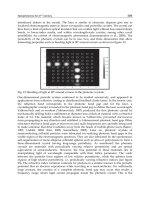
In Fig. 1 a SET equivalent circuit is displayed. First, it is helping to write the equations for a
double junction system, and then to correct them when a gate contact is added.
The charge q
i
at the i-th junction can be written as q
i
=C
i
V
i
, so, the total charge into the island
is q= q
2
-q
1
+q
0
=-ne+q
0
where q
0
is the background charge inside the island and n=n
1
-n
2
is an
integer number indicating the electrons in excess.
Fig. 1. Equivalent circuit of a single-island, two-junctions SET
The voltage bias across the i-th junction is then:
()
()
()
1
0
3
1
i
iSD
i
VCV qneC
−
Σ
−
=+−−
(6)
where V
SD
is the bias across the device (V
SD
= ΣV
i
) and C
Σ
=ΣC
i
.
To add the contribution of the gate contact in the device, we can simply take into account
for effect of the gate electrode on the background charge q
0
. This quantity can be changed
at will, because the gate additionally polarizes the island, so that the island charge
becomes:
Current Status and Technological Limitations
of Hybrid Superconducting-Normal Single Electron Transistors
283
()
02gg
q
ne
q
CV V=− + + − (7)
with V
g
the gate voltage.
Now, after, some trivial calculations, one can write the final relationship giving the voltage
bias across the i-th junction in Single Electron Transistor (SET) composed by 1 island
surrounded by 2 tunnel junctions:
()
() ()
{
}
1
1
,1 0
3
11
ii
igiSDgg
i
VC C C V CV ne
q
δ
+
−
Σ
−
= + +− +− +
(8)
where δ
i,1
is the Dirac’s function and C
Σ
=ΣC
i
+C
g
.
By combining (8) and (5) it is possible to explicitly write the equations governing the free
energy change in a system with two tunnel junctions and a gate electrode. For example,
under the particular conditions: q
0
= 0, R
1
= R
2
and C
1
= C
2
= C>> C
g
, one gets:
()
1
2 1/2 /2
cg SD
FEnn V
±
Δ= ± + ±
()
2
2 1/2 /2
cg SD
FEnn V
±
Δ= ±+ ± (9)
where n
g
=C
g
(V
g
-V
2
) and E
c
=e
2
/2C.
In order to model the behavior of such a complex system, some simplifying assumptions are
needed. First of all, we consider the tunneling events as instantaneous and uncorrelated,
say, one is occurring at a time. Since any single-electron tunneling event changes the charge
state of the island, at least two states are required for current transport.
Having the rates of tunneling through the two junctions at hand we can now define the rates
of elementary charge variation for the island as:
12
1,
() ()
nn
nn
+
Γ=Γ+Γ
21
1,
() ()
nn
nn
−
Γ=Γ+Γ
(10)
With the aid of the above considerations it is possible to define a master equation that
governs the behavior of the system, whose solution is (Ingold & Nazarov, 1992):
,1 1 1,nn n n n n
PP
++ +
Γ=Γ (11)
where P
n
is the probability distribution for the island charge state.
Taking as a starting state that one with no excess charge in the island and considering that
only the nearest neighbors states are connected by non-null rates, the probability
distribution can be derived from eq. (11) as:
1
01,,1
0
/
n
nmmmm
m
PP
−
++
=
=ΓΓ
∏
n > 0
0
01,,1
1
/
nmmmm
mn
PP
−−
=+
=ΓΓ
∏
n < 0
(12)
where the free parameter P
0
can be extracted from the normalization condition 1
n
P
+∞
−∞
=
.
Being the steady-state currents through the two junctions equal to I we can write:
Superconductivity – Theory and Applications
284
11 22
() () () ()
nn
IeP n n eP n n
+∞ +∞
−∞ −∞
=Γ−Γ=Γ−Γ
(13)
It’s trivial to note that in the T=0 limit the terms (
11
Γ−Γ
and
22
Γ−Γ
) of eq. (13) are
identically null for some values of V
SD
and n
g
. In these states it is also noted that the
probability distribution P
n
=1 for a well defined value of n. This means that these regions are
stable in terms of the number of charges on the island and both tunnel junctions are in the
so-called Coulomb Blockade state.
In the zero temperature limit, by imposing
0
i
F
±
Δ=
, one is able to write down the equations
providing the dependence of V
SD
on n
g
at the boundaries between the regions in which
tunneling is allowed (
0
i
F
±
Δ<
) and forbidden (
0
i
F
±
Δ>
). Without going into details on this
rather simple calculation, we can easily observe that such dependence is linear, with slopes
given by
()
,1
3
/
ggi
i
CC C
−
+δ
and intercepts related to the number n of excess electrons into
the island. These lines give rise to the well-known Stability Diagram for a n-SET depicted in
Fig. 2.
Diamonds in the Stability Diagram are representative for the region where tunneling is
inhibited (
0
i
F
±
Δ>
). They are defined by two families of parallel lines having positive (1st
junction) and negative (2nd junction) slopes, respectively. Outside such regions, current can
flow freely across the device, whereas the control of the charging state at single-electron
level can be obtained only when the working point with coordinates n
g
,V
SD
lies inside a
stable diamond.
Fig. 2. Stability Diagram for a n-SET
Current Status and Technological Limitations
of Hybrid Superconducting-Normal Single Electron Transistors
285
It is important to stress that the stable states in the case of n-SETs have a single degeneracy
point in which the the states with n or n +1 are equiprobable (Fig. 2).
The only location on the stability diagram, and therefore the only set of coordinates n
g
,V
SD
which allows the system to switch from one stable state to another passes through the
degeneracy point where the bias voltage V
SD
is nil in any circuit configuration. Then, the
reader can understand how a simple n-SET can control the number of elementary charges in
excess on the island, solely, but not the flow of single electrons from source to drain
electrodes. This because the system switch from n to n +1 can occur either through the
forward tunneling in the first junction or the backward tunneling in the second junction,
with the same probability. In other words, V
SD
=0 implies that no directionality for the events
is defined, that is, the n-SET cannot work as a turnstile.
For V
SD
≠ 0, the current can freely flow across the device in well-defined V
g
intervals. The
so-called SET oscillations can then be observed (Fig. 3).
Investigators have tried to circumvent this problem by using multi-island electron pumps
(Zimmerman & Keller, 2003). In such devices some islands are in series and driven by their
own gate contact. Sinusoidal waveforms for each of these gates are shifted in phase, so to
ensure that successive tunnel process occur from the first to the last junction. The relatively
complicated experiment with such a slow device yields an output value for the singular
current much lower than the limit (10
-10
-10
-9
A) necessary for carrying out the Metrological
Triangle experiment with the required accuracy.
Fig. 3 The SET oscillations occurring when V
SD
≠ 0. Values for V
SD
are given on the right side
of the Fig. With scanning V
g
, we find peaks representing the current flow through the
device, when
0
i
F
±
Δ<
(outside of the diamonds in Fig. 2), and minima related to
0
i
F
±
Δ>
.
Superconductivity – Theory and Applications
286
2.3 The hybrid SET
Hybrid superconducting-metal assemblies have been recently proposed and shown to be
capable of higher accuracy (Pekola et al., 2008). From a technological point of view, this
assembly is composed by a normal-metal island sandwiched by two superconducting
electrodes (SNS), or the reverse (NSN) scheme. For the purpose of this chapter, the
theoretical description is the same for both the arrangements.
In the following chapter, eqs. (4) will be rewritten in the case of NIS junction and applied to
h-SET.
2.3.1 Tunneling in a S-I-N junction
Typical applications of SIN junctions are microcoolers (Nahum et al., 1994; Clark et al., 2005;
Giazotto et al., 2006)
and thermometers (Nahum & Martinis, 2003; Schmidt et al. 2003;
Meschke et al. 2006; Giazotto et al., 2006). In these applications, SIN junctions are usually
employed in the double-junction (SINIS) geometry. The opposite NISIN geometry has
gathered less attention. Recently, there has been interest in SINIS structures with
considerable charging energy. They have been proposed for single-electron cooler
applications (Pekola et al., 2007; Saira et al., 2007) that are closely related to the quantized
current application (Pekola et al., 2008). Thermometry in the Coulomb-blocked case has
been considered, too (Koppinen et al., 2009).
In the case where the superconductor in study is well below its transition temperature
(T
S
<T
c
) it can be assumed for the superconducting gap Δ that Δ(T
S
)=Δ(0) = Δ.
Because the number of particles for a given amount of energy must be the same in the
superconducting state (quasi-particles) and in the normal one (free electrons), the
relationship:
() ()
sn
gEdE g d
εε
=
(14)
must hold, and then:
()
()
1/2
22
() ()
sn
gE g EE E
εθ
−
=−Δ−Δ
(15)
where θ is the Heaviside’s step function.
Then, the density of states in a superconductor can be written as:
()
()
1/2
22
() (0)
sn
gE g EE E
θ
−
≅−Δ−Δ (16)
by considering that:
1.
all the energy terms at low temperatures have significant values of the order of k
B
T
(which is several orders of magnitude less than the Fermi energy, k
B
T<<E
F
);
2.
the energies are measured with respect to the Fermi level (ε=0 at E
F
);
3.
() (0)
nn
gg
ε
≈
.
A further assumption is that the electrons in the metal and the quasiparticles in
superconductor are weakly interacting and at thermal equilibrium due to the high potential
barrier of the dielectric layer. It is then possible, to consider tunneling as a perturbation and
to apply the Golden Rule approach. The dominating current transport mechanism in a NIS
junction is single-electron tunneling between the normal metal and the quasi-particle states
of the superconductor.
Current Status and Technological Limitations
of Hybrid Superconducting-Normal Single Electron Transistors
287
The equations governing the rate of tunneling back and forth in a NIS can be written in a
similar way to that for the NIN system by simply adding a term proportional to the
superconductor density of states:
()
21
(, )1 ( , )eR n E fET fE FT dE
Ts S N
−+
+∞
Γ= − −Δ
−∞
()
21
(,)1(,)eR n EfE FT fET dE
Ts N S
−−
+∞
Γ= +Δ −
−∞
(17)
where T
s
and T
N
are temperatures for the superconductor and normal electrodes,
respectively and n
s
=g
s
(E)/g
N
(0).
For T = 0, the corresponding of eq. (4.3) is found for the SIN case:
21 2 2
T
eR F
−−
Γ= Δ −Δ
FΔ≤−Δ
(18)
whereas Γ= 0 for ΔF>-Δ (the other two solutions cannot be considered because transitions
are allowed only for negative free energy variations).
Finding a solution for eq. (17) is not a trivial task and will not be reported here, but some
words are deserved to the tunneling effects occurring in the SIN junction at voltages values
below gap. Here, if the condition K
b
T
N
<<ΔF (i.e., if T
N
<<1.76 T
c
) is fulfilled, the rate of
tunneling through the SIN junction is given by:
()
()
0
,exp /
TN bN
VT F kTΓ=Γ Δ−Δ
(19)
the quantity
21
0
/2
TbN
eR kT
π
−−
Γ=Δ Δ
being called the characteristic rate and
approximately representing the tunneling rate when the free energy variation approaches
the gap.
From eq. (19) it can be seen that for free energy variations below the gap the tunneling rate
strongly depends on temperature. This opens the possibility of using this type of junction as
a thermometer at low temperature. As a drawback, limits in the accuracy of electron
counting for metrological applications of h-SETs can arise, as discussed in the next chapters.
2.3.2 Stability diagram for h-SET
Following the same n-SET master equation approach for the SINIS system, it is now possible
to combine eqs. (9) and (17) in order to consider the case in which the mesoscopic tunnel
junctions charging energy is not negligible and the central island is coupled to a gate
electrode.
Results from calculations of the electrical characteristics for the previous ideal system are
shown in Fig. 4. Using a similar procedure for the n-SET device we can study the h-SET
behavior at temperature T->0 K in order to extract the modified stability diagram.
It is observed from eq. (18) that when ΔF > -Δ, the tunneling rate is nil (in principle) and the
junction does not allow for the electron flow. The areas in the stability diagram in which
such conditions hold identify the stable regions with a defined number of elementary
charges on the island (n).
Superconductivity – Theory and Applications
288
Fig. 4. 3-dimensional view of the Stability Diagram for a h-SET
The present formalism allows us to treat the hybrid assembly in the same way as the normal
system. Then, very trivial calculations let us to extract the equations for the two families of
straight lines defining the boundaries between regions of allowed and forbidden tunneling,
with an offset value with respect to the lines in the normal case of 2Δ (Fig. 5).
The dashed lines in Fig. 5 define the regions of inhibited tunneling, as in the case of the
n-SET (purple areas). In the hybrid system, each of them is shifted by an offset 2Δ, defining
the blue regions where the mechanism of tunnel inhibition is the band offset at the SIN
junction.
When the Current across a Single Electron Tunneling device is recorded as a function of the
V
SD
, for different n
g
values, a family of Current-Voltage characteristics is obtained. This
means we are moving along parallel vertical pathways on the Stability Diagram. The
extension of the Coulomb gap, obviously depends on the n
g
value: in a Normal SET it
periodically oscillates from 0 to e/2C, with a periodicity of one unit (see Fig. 6).
It is then interesting to compare the Current-Voltage characteristics of the Normal and
Hybrid SETs. This comparison, reported in Fig. 6, clearly indicates a broadening of the
conduction gap in the hybrid structure. The gap oscillates with tuning V
g
from ∆ to
∆+ e/2C. In a few words, the presence of the superconducting gap broadens the region of
inhibited tunneling, whose width never equals to zero.
In this configuration for the h-SET, the degeneracy point linking the stable states is
suppressed by a region in the V
SD
—n
g
space where the pathway from point A to point B
occurs with negligible backward tunneling at both junctions (V
SD
> 0) and without departing
from the stable regions. E.g., with V
g
oscillating between the states A and B, one can move a
single electron per cycle from source electrode to drain with a well defined directionality
given by the sign of V
SD
.