Optoelectronics Devices and Applications Part 12 pot
Bạn đang xem bản rút gọn của tài liệu. Xem và tải ngay bản đầy đủ của tài liệu tại đây (2.98 MB, 40 trang )
Electromechanical Fields in Quantum Heterostructures and Superlattices 11
4. Quantum structures
The key issue for investigating piezoelectric effects in the wurtzite and zincblende crystal
structures is their widespread use in optoelectronics and electronics in general. Here we
will focus on "clean" quantum structures, i.e. without doping. The major reason for the
use of materials such as GaN, AlN and others is their large electronic band gap creating the
possibility of large energy transitions as necessary for UV-leds. A basic sketch of a quantum
well structure is shown in Figure5
(1) (1)(2)
E
(2)
g
E
(1)
g
Fig. 5. Basic sketch of a quantum well structure. The indices (1) and (2) denote barrier and
well material, respectively. The upper part indicates the conduction and valence band
energies for zero electric field.
The three types of quantum structures that differ in the number of confined dimensions are
• Quantum well: one dimension confined
• Quantum wire: two dimensions confined
• Quantum dot: three dimensions confined
One motivation for investigation of these types is that a decrease of dimensionality is reflected
in the density of state functions of these structures. The dependency of the density of states
(DOS), denoted N
(E), on the energy E functions read in a one-band effective model (Singh,
2003)
N
(E)
bulk
=
√
2m
∗3/2
√
E − E
c
π
2
¯h
3
, (37)
N
(E)
well
=
m
∗
π¯h
2
; E > E
i
(from each subband i), (38)
N
(E)
wire
=
√
2m
∗1/2
π¯h
(E − E
i
)
−1/2
; E > E
i
(from each subband i), (39)
N
(E)
dot
= δ(E − E
i
), (40)
where E
c
is the conduction band energy and m
∗
is the electron effective mass. Note that the
DOS for a quantum dot is discrete, i.e. a quantum dot is treated as a single, isolated particle.
A thorough discussion about these three structures can be found in Singh (2003).
The theory presented in this chapter covers electromechanical fields of both well and barrier
structures, the latter being used for transistor technology (Koike et al., 2005; Sasa et al., 2006).
429
Electromechanical Fields in Quantum Heterostructures and Superlattices
12 Will-be-set-by-IN-TECH
5. One-dimensional electromechanical fields in quantum wells
This section contains an example for the application of the above equations on quantum wells.
For simplicity we will assume no free charges in the structure as this removes the necessity of
solving the Schrödinger equation simultaneously.
The well layer
(2) will adapt its lattice constant to the barriers (1) and the strain in the well
layer is defined as (Ipatova et al., 1993)
S
(2)
=
⎡
⎢
⎢
⎢
⎢
⎢
⎢
⎢
⎢
⎢
⎢
⎢
⎢
⎢
⎢
⎢
⎢
⎢
⎣
∂u
(2)
x
∂x
− a
mis
∂u
(2)
y
∂y
− a
mis
∂u
(2)
z
∂z
−c
mis
∂u
(2)
y
∂z
+
∂u
(2)
z
∂y
∂u
(2)
x
∂z
+
∂u
(2)
z
∂x
∂u
(2)
x
∂y
+
∂u
(2)
y
∂x
⎤
⎥
⎥
⎥
⎥
⎥
⎥
⎥
⎥
⎥
⎥
⎥
⎥
⎥
⎥
⎥
⎥
⎥
⎦
, (41)
while the strain in layer
(1) is defined as usual (see equation (1)). This definition is for
wurtzite structures, having two lattice constants a, c. The mismatch a
mis
is given by a
mis
=
a
(2)
− a
(1)
/a
(1)
and c
mis
is defined similarly. For use with zincblende, c
mis
= a
mis
.
For the quantum well it is often assumed that all quantities depend exclusively on the
z-direction and the x, y-directions are infinite. Note that, since we are working with first
order strain, the choice of the denominator for a
mis
and c
mis
is arbitrary, as the difference
a
(2)
− a
(1)
/a
(1)
−
a
(2)
− a
(1)
/a
(2)
is of second order.
5.1 Crystal orientation
As already discussed, the zincblende structure does not exhibit piezoelectric properties upon
hydrostatic compression (i.e. no shear). However, as seen in Figure 1 there is reason to
believe that a rotation of the crystal structure yields a piezoelectric field upon hydrostatic
compression.
The rotation of unit cells is modeled by a rotation of the describing coordinate system
transforming coordinates x, y, z
→ x
, y
, z
. The transformation is performed by two
subsequent rotations around coordinate axis as shown in Figure 6. The different quantities
then transform as
r
= a ·r, P
SP
= a ·P
SP
,
T
= M ·T, S
= N ·S,
E
= a ·E, D
= a ·D,
ε
= a ·ε ·a
T
, e
= a ·e ·M
T
,
c
E
= M ·c
E
·M
T
,
430
Optoelectronics – Devices and Applications
Electromechanical Fields in Quantum Heterostructures and Superlattices 13
x
z, z
φ
x
φ
y
φ
φ
φ
y
x
y
z, z
φ
x
φ
,x
y
φ
y
y
z
θ
θ
Fig. 6. Subsequent coordinate system rotations - φ around z followed by θ around the new
x-axis. The cubes to the left indicate the cubic crystal structure while the middle and right
figures represent the same operation for hexagonal crystals. Reprinted with permission
from Duggen et al. (2008) and Duggen & Willatzen (2010).
where a is given by (Auld, 1990; Goldstein, 1980)
a
=
⎡
⎣
cos
(φ) sin(φ) 0
−cos(θ) sin(φ) cos(θ) cos(φ) sin(θ)
sin(θ) sin(φ) −sin(θ) cos(φ) cos(θ)
⎤
⎦
, (42)
and the M, N matrices are called Bond stress and strain transformation matrices, respectively.
They are constructed out of the elements of a as given in the following (Auld, 1990; Bond,
1943):
M
=
⎡
⎢
⎢
⎢
⎢
⎢
⎢
⎢
⎢
⎢
⎢
⎣
a
2
11
a
2
12
a
2
13
2a
12
a
13
2a
13
a
11
2a
11
a
12
a
2
21
a
2
22
a
2
23
2a
22
a
23
2a
23
a
21
2a
21
a
22
a
2
31
a
2
32
a
2
33
2a
32
a
33
2a
33
a
31
2a
31
a
32
a
21
a
31
a
22
a
32
a
23
a
33
a
22
a
33
+ a
23
a
32
a
21
a
33
+ a
23
a
31
a
22
a
31
+ a
21
a
32
a
31
a
11
a
32
a
12
a
33
a
13
a
12
a
33
+ a
13
a
32
a
13
a
31
+ a
11
a
33
a
11
a
32
+ a
12
a
31
a
11
a
21
a
12
a
22
a
13
a
23
a
12
a
23
+ a
13
a
22
a
13
a
21
+ a
11
a
23
a
11
a
22
+ a
12
a
21
⎤
⎥
⎥
⎥
⎥
⎥
⎥
⎥
⎥
⎥
⎥
⎦
, (43)
N
=
⎡
⎢
⎢
⎢
⎢
⎢
⎢
⎢
⎢
⎢
⎢
⎣
a
2
11
a
2
12
a
2
13
a
12
a
13
a
13
a
11
a
11
a
12
a
2
21
a
2
22
a
2
23
a
22
a
23
a
23
a
21
a
21
a
22
a
2
31
a
2
32
a
2
33
a
32
a
33
a
33
a
31
a
31
a
32
2a
21
a
31
2a
22
a
32
2a
23
a
33
a
22
a
33
+ a
23
a
32
a
21
a
33
+ a
23
a
31
a
22
a
31
+ a
21
a
32
2a
31
a
11
2a
32
a
12
2a
33
a
13
a
12
a
33
+ a
13
a
32
a
13
a
31
+ a
11
a
33
a
11
a
32
+ a
12
a
31
2a
11
a
21
2a
12
a
22
2a
13
a
23
a
12
a
23
+ a
13
a
22
a
13
a
21
+ a
11
a
23
a
11
a
22
+ a
12
a
21
⎤
⎥
⎥
⎥
⎥
⎥
⎥
⎥
⎥
⎥
⎥
⎦
. (44)
Note that we have chosen to let the third rotation angle ψ to be zero, as this is a rotation about
the z
-axis and does not alter the growth direction. In the following the primes are omitted.
It is also noteworthy that calculations for wurtzite show that all the material parameter tensors
as well as the misfit strain contributions do not depend on the angle φ (Bykhovski et al., 1993;
Chen et al., 2007; Landau & Lifshitz, 1986).
431
Electromechanical Fields in Quantum Heterostructures and Superlattices
14 Will-be-set-by-IN-TECH
5.2 Static case
In the static case the equations to solve in each layer become
∇·T
(i)
= 0, ∇·D
(i)
= 0, ∇×E
(i)
= 0
→
∂T
(i)
3
∂z
=
∂T
(i)
4
∂z
=
∂T
(i)
5
∂z
= 0, →
∂D
(i)
z
∂z
= 0, →
∂E
(i)
x
∂z
=
∂E
(i)
y
∂z
= 0, (45)
where the superscript i denotes the material, as depicted in Figure 5. Usually one would use
homogeneous Dirichlet boundary conditions for the electric field E
x
|
z=z
l
,z
r
= E
y
|
z=z
l
,z
r
= 0,
corresponding to the case where the two ends are covered by a perfect conductor. As electric
coupling conditions force continuity of the tangential components of E and these components
are constant in each layer we obtain E
x
= E
y
= 0 everywhere. Using the definition of strain
we find that in each layer
∂
2
u
x
∂z
2
=
∂
2
u
y
∂z
2
=
∂
2
u
z
∂z
2
, (46)
that is, we have linear solutions for the displacement in each layer:
u
i
= A
(j)
i
z
+ B
(j)
i
. (47)
These coefficients are then found by applying continuity of
T
3
, T
4
, T
5
, u
x
, u
y
, u
z
,andD
z
(48)
at the material interfaces. At the outer boundaries we will assume free ends
T
5
= T
4
= T
3
= 0, D
z
= D. (49)
The conditions for clamped ends would be u
x
= u
y
= u
z
= 0attheends.TheparameterD
is a degree of freedom that in principle corresponds to the application of a voltage across the
outer ends (as it changes the electric field and in the static case the electric potential is merely
an integration over space). Calculations for a superlattice structure (i.e. a periodic repetition
of well and barriers) are exactly the same, with the lattice constants in the well layers adapting
to those of the barrier (Poccia et al., 2010).
Calculations for the
[111] growth direction of zincblende crystals yields the following
analytical expression for the compressional strain in the quantum well (Duggen et al., 2008):
S
zz
=
2
√
3
e
(2)
x4
(2)
D + 3
c
(2)
11
+ 2c
(2)
12
a
mis
4
e
(2)
2
x4
(2)
+ c
(2)
11
+ 2c
(2)
12
+ 4c
(2)
44
− a
mis
. (50)
Results for the
[111] direction in zincblende quantum wells, with several materials, are given
in Table 1. The
[111] direction is a rather special case as a compression in the [111] direction
yields an electric field in the
[111] direction as well and this direction does not couple to the
transverse components (i.e. a compression in z-direction does not generate an electric field
in x or y directions.) - here zincblende behaves very similar to wurtzite grown along the
432
Optoelectronics – Devices and Applications
Electromechanical Fields in Quantum Heterostructures and Superlattices 15
[0001] direction. The table also contains a comparison between the fully and the semi-coupled
model. The terms S
semi
and S
cou pling
refer to semi-coupled result and the difference to the fully
coupled result, respectively, i.e. S
fully−co u pled
= S
semi
+ S
cou pling
.
substrate/QW S
semi
S
cou pling
Deviation E
z,t
[V/μm] E
z,e
[V/μm]
GaAs/In
0.1
Ga
0.9
As 0.34% −0.002% 0.5% 15.56 17 ±1
a
GaAs/In
0.2
Ga
0.8
As 0.710% −0.003% 0.4% 28.63 25
b
AlN/GaN 1.34% −0.04% 3.1% 271.6
GaN/In
0.3
Ga
0.7
N 1.69% −0.07% 4.4% 355.0
GaN/InN 7.24%
−0.61% −9.1% 1441.5
GaN/AlN
−0.91% 0.04% −4.7% −280.3
a
Caridi et al. (1990)
b
J.I.Izpura et al. (1999)
Table 1. Contributions to S
zz
in the [111]-grown quantum well layer for different zincblende
material compositions with D
= 0. For GaAs/In
x
Ga
1−x
As both E
z,t
and E
z,e
,beingthe
theoretical and the experimental electric field in the QW-layer respectively, are listed for
comparison
It can be seen that it does not play a role whether one uses the fully-coupled or the semi
coupled approach for the nitrides. Note, however, that the electric field generated by the
intrinsic strain in the quantum well layer is quite large and will definitely have an influence
on the electrical properties.
The same calculations have been carried out for wurtzite quantum wells (and barriers). For
the
[0001] growth direction, the analytic result for the compressional strain, which is not
coupled to the shear strains in this case, reads (Duggen & Willatzen, 2010; Willatzen et al.,
2006)
S
xx
= S
yy
= −a
mis
, (51)
S
(1)
zz
= e
(1)
z3
D − P
(1)
z
e
(1)
2
z3
+ c
(1)
33
(1)
zz
, (52)
S
(2)
zz
=
e
(2)
z3
(D − P
(2)
z
)+2a
mis
(e
(2)
z1
e
(2)
z3
+ c
(2)
13
(2)
zz
)
e
(2)
2
z3
+ c
(2)
33
(2)
zz
, (53)
In principle one can of course find analytic expressions for the general strains as function of
the two angles φ, θ (for both wurtzite and zincblende). However, these expressions are very
cumbersome to comprehend and therefore do not provide additional insight.
Results for the growth direction dependency of a GaN/Ga
1−x
Al
x
N/GaN well are shown
in Figure 7. For this structure the shear strain is negligible and therefore omitted. For
other materials, however the shear strain component is significant and there are significant
differences between the fully and semi-coupled approach as seen in Figure 8.
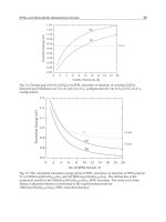
Note that for sufficiently large Al-content, the electric field in the GaAlN well becomes zero
at two distinct angles. For the MgZnO structures it shows that there even exist up to three
distinct zeros (Duggen & Willatzen, 2010). This is of potential importance as it might lead to
increased efficiency for the application of white LEDs (Waltereit et al., 2000).
433
Electromechanical Fields in Quantum Heterostructures and Superlattices
16 Will-be-set-by-IN-TECH
0 20 40 60 80
−2
−1
0
1
2
θ [degrees]
S
zz
(2)
[%]
0 20 40 60 80
0
5
10
15
θ [degrees]
E
z
(2)
[MV/cm]
Fig. 7. Compressional strain S
(2)
zz
(left) and electric field E
z
(2) (right) for
GaN/Ga
1−x
Al
x
N/GaN with several x-values and D = 0C/m
2
. The colors blue, red, green,
black, and magenta correspond to x
= 1, x = 0.8, x = 0.6, x = 0.4, and x = 0.2, respectively.
Solid (dashed) lines correspond to the semi-coupled (fully-coupled) model. Reprinted with
permission from Duggen & Willatzen (2010)
0 20 40 60 80
0
1
2
3
4
θ [degrees]
S
yz
(2)
[%]
Semi coupled
Fully coupled
0 20 40 60 80
−4
−2
0
2
4
θ [degrees]
S
zz
(2)
[%]
Semi coupled
Fully coupled
Fig. 8. Shear strain component S
(2)
yz
(left) and compressional strain component S
2
zz
(right) in
the quantum-well layer of a Mg
0.3
Zn
0.7
O/ZnO/Mg
0.3
Zn
0.7
O heterostructure for the
fully-coupled and semi-coupled models corresponding to D
= 0C/m
2
. Reprinted with
permission from Duggen & Willatzen (2010)
5.3 Monofrequency case
Both single quantum wells and for superlattice structures might be subject to an applied
alternating electric field, which we will model as application of a monofrequent D-field, i.e.
we will assume time harmonic solutions ∝ exp
(iωt),whereω = 2π f and f is the excitation
frequency. Here we will limit us to the zincblende case, but the theory is just as well applicable
to wurtzite structures, where one needs to take into account the spontaneous polarization P
SP
as well.
As the coupling conditions are continuity of T, it is convenient to derive the corresponding
differential equation for T. As we assume only z-dependency, Navier’s equation becomes
three equations:
∂T
I
∂z
= ρ
m
∂
2
u
i
∂z
, (54)
434
Optoelectronics – Devices and Applications
Electromechanical Fields in Quantum Heterostructures and Superlattices 17
where I, i are 3, z,4,y,5,x. Furthermore we have that
∂S
I
∂t
=
∂
2
u
i
∂t∂z
, (55)
with the same pairs I, i. Differentiating with respect to z and t, respectively, combining and
eliminating u we obtain
∂
2
T
I
∂z
2
= ρ
m
∂
2
S
I
∂t
2
. (56)
Then using the piezoelectric fundamental equation along with the electrostatic approximation
(forcing E
x
= E
y
= 0 as in the static case) we obtain the set of three coupled wave equations:
Γ
33
∂
2
T
3
∂z
2
+ Γ
34
∂
2
T
4
∂z
2
+ Γ
35
∂
2
T
5
∂z
2
−ρ
m
∂T
3
∂t
2
= ρ
m
e
T
3z
S
∂
2
D
z
∂t
2
, (57)
Γ
43
∂
2
T
3
∂z
2
+ Γ
44
∂
2
T
4
∂z
2
+ Γ
45
∂
2
T
5
∂z
2
−ρ
m
∂T
4
∂t
2
= ρ
m
e
T
4z
S
∂
2
D
z
∂t
2
, (58)
Γ
53
∂
2
T
3
∂z
2
+ Γ
54
∂
2
T
4
∂z
2
+ Γ
55
∂
2
T
5
∂z
2
−ρ
m
∂T
5
∂t
2
= ρ
m
e
T
5z
S
∂
2
D
z
∂t
2
, (59)
where Γ is the piezoelectrically stiffened elastic tensor. Note that the dispersion relation
(which is above equations with D
z
= 0) is the same as in equation (35) with the weak coupling
terms removed as is done with the electrostatic approximation.
The general solution to these wave equations consist of forward and backward propagating
waves.Thesolutionineachlayerfore.g.thex-polarization reads
T
(i)
5
= T
(i)
5A+
exp(ik
1
z)+T
(i)
5A−
exp(−ik
1
z)+T
(i)
5B+
exp(ik
2
z)+T
(i)
5B−
exp(−ik
2
z)
+ T
(i)
5C+
exp(ik
3
z)+T
(i)
5C−
exp(−ik
3
z) −
e
(i)T
5z
S(i)
D
z
. (60)
The other polarizations can then be found by solving the dispersion relation for T
3
(k)/T
5
(k)
and T
4
(k)/T
5
(k).Thus,whentheT
5
amplitudes are known, all amplitudes are known. The
coupling conditions between the layers are continuity of stress and continuity of particle
velocity (corresponding to continuity of particle displacement in the static case), with the
particle velocity v given by
v
=
1
ρ
m
ω
∂T
∂z
, (61)
where a comment about the dimensionality of v should be made, since obviously we get
elements v
zx
, v
zy
, v
zz
. This is consistent, as the wave has propagation direction z,but
three different polarizations x, y, z,i.e. v
5
, v
4
describe shear waves while v
3
describes a
compressional wave.
The collection of boundary condition equations yields an 18
×18 matrix with exp(ik
1
z
1
)-like
entries. If one would solve for a superlattice consisting of n layers, one would need to solve
a6n
×6n system of equations. As for superlattices this becomes useful when e.g. wanting to
435
Electromechanical Fields in Quantum Heterostructures and Superlattices
18 Will-be-set-by-IN-TECH
compute a macroscopic speed of sound as one can find resonance frequencies and compare to
the expression for resonance frequencies of a homeogeneous material. Note that the intrinsic
strain will change the bulk speed of sound of the well material, so one cannot simply use a
weighted average of the two sound velocities. Furthermore it is expected that operation at
resonance strongly influences the properties of the structure (Willatzen et al., 2006).
The first five resonance frequencies for a zincblende AlN/GaN are shown in Figure 9.
It is seen that the transversely dominated resonances (only at
[111] the, at this direction
degenerate, transverse polarizations are uncoupled from the compressional one) are much
lower than the compressionally dominated ones, as one would expect. Thus, when computing
resonance frequencies it is important not to compute the ideal
[111] direction only, but
also take into account the significantly lower frequencies as they might occur due to lattice
imperfections (Duggen et al., 2008).
−pi/2 [111]−pi/4 0
10
15
20
25
30
35
40
θ [rad]
Resonance frequency [GHz]
Transverse
Longitudinal
Fig. 9. The first five resonance frequencies for the AlN/GaN structure with φ = −π/4. The
dimensions of the well-strucure used are 100nm-5nm-100nm. Reprinted with permission
from Duggen et al. (2008)
5.4 Cylindrical symmetry of [0001] wurtzite
As we have already noted, the material parameter matrices are invariant under rotation
of an angle φ around the z-axis. This stipulates investigations of cylindrical structures of
wurtzite type. The calculations can, in principle, be done exactly the way described for the
quantum well. However, here we consider two degrees of freedom (r, z) which complicates
the differential equations and it might not be possible to find analytic solutions anymore.
The Voigt notation follows the same standard as for the Cartesian coordinates (including the
weight factors) and are
rr
→ 1, φφ → 2, zz → 3, φz → 4, rz → 5, rφ → 6. (62)
The divergence operator becomes
∇· →
⎡
⎢
⎣
∂
∂r
+
1
r
−
1
r
00
∂
∂z
1
r
∂
∂φ
0
1
r
∂
∂φ
0
∂
∂z
0
∂
∂r
+
2
r
00
∂
∂z
1
r
∂
∂φ
∂
∂r
+
1
r
0
⎤
⎥
⎦
, (63)
436
Optoelectronics – Devices and Applications
Electromechanical Fields in Quantum Heterostructures and Superlattices 19
and the material property matrices are transformed in the same manner as for crystal
orientation, with
a
=
⎡
⎣
cos
(φ) sin(φ) 0
−sin(φ) cos(φ) 0
001
⎤
⎦
, (64)
so since there is cylindrical symmetry, the material parameter matrices remain unchanged.
Again using Navier’s equation and
∇·D = 0 one obtains the following linear system of
differential equations (with all φ-dependencies neglected) (Barettin et al., 2008):
L
·
⎡
⎣
u
r
u
z
V
⎤
⎦
=
⎡
⎣
−∂
r
[
(
C
11
+ C
12
)a
mis
+ C
33
c
mis
]
−
∂
z
[
2C
13
a
mis
+ 2C
13
c
mis
]
−
∂
z
p
SP
⎤
⎦
, (65)
L
=
⎡
⎣
∂
r
C
11
∂
r
+ ∂
z
C
ee
∂
z
+ 1/r∂rC
12
+ c
11
∂
r
1/r
∂
r
C
44
∂
z
+ ∂
z
C
13
∂
r
+ ∂
z
C
13
/r + c
44
/r∂
z
∂
r
e
15
∂
z
+ e
15
/r∂
z
+ ∂
z
e
31
∂
r
+ ∂
z
e
15
/r
⎤
⎦
·
100
+
⎡
⎣
∂
r
C
13
∂z + ∂
z
C
44
∂r
∂
r
C
44
∂
r
+ ∂
z
C
33
∂
z
+ C
44
/r∂r
∂
r
e
15
∂
r
+ e
15
/r∂r + ∂
z
e
33
∂
z
⎤
⎦
·
010
+
⎡
⎣
∂
r
e
31
∂
z
+ ∂
z
e
15
/r∂
r
∂
r
e
33
∂
z
+ ∂
z
e
13
∂
r
+ e
15
/r∂
r
−∂
r
11
∂
r
−∂
z
33
∂
z
−
11
/r∂
r
⎤
⎦
·
001
, (66)
where ∂
i
is short notation for ∂/∂i and V is the electric potential (thus E
z
= −∂
z
V). This
system can be solved numerically e.g. by using the Finite Element Method. This has been
done for a cylindrical quantum dot structure sketched in Figure 10
Fig. 10. Geometry of the system under consideration (left) and the two-dimensional
equivalent (right). Reprinted with permission from Barettin et al. (2008)
They have found, as can be seen in Figure 11, that the major driving effect for the strain is the
lattice mismatch and not the spontaneous polarization.
437
Electromechanical Fields in Quantum Heterostructures and Superlattices
20 Will-be-set-by-IN-TECH
Fig. 11. Displacements u
r
at z = 0(left)andu
z
at r = 0. Four modeling cases are depicted. It
suffices to say that only case three does not consider lattice mismatch contributions.
Reprinted with permission from Barettin et al. (2008)
Furthermore, using basically the same calculations, Lassen, Barettin, Willatzen & Voon (2008)
revealed that calculations in the 3D case can yield a substantially larger discrepancy between
semi and fully coupled models, where in the GaN/AlN differences up to 30% were found.
5.5 Other effects
It should be noted that the method described above is by no means secure to be absolutely
correct. For example we have disregarded possible free charge densities in order to solve
the electromechanical equations self-consistently, without having to solve the Schrödinger
equation simultaneously, which would have been necessary otherwise (Voon & Willatzen,
2011). However, it was found by Jogai et al. (2003) that there exists a 2D-electron gas at
the interfaces, effectively reducing the generated electric field. Thus the necessity of a fully
coupled model is not automatically given, even though calculations as above indicate it.
Also, as already indicated in the piezoelectricity section there might be non-linear effects that
are of importance. According to Voon & Willatzen (2011) the effect of non-linear permittivity
can be neglected in spite of large electric fields. However, it is not sure whether electrostrictive
or second order piezoelectric effects might be of importance. Clearly these questions need
further research in order to improve the understanding of electromechanical effects in these
structures.
5.6 Alternative: VFF method
As opposed to the above, semi-classical approach there also exist atomistic methods of
calculating strains in quantum structures. The are called Valence Force Field (VFF) methods
of which Keatings model is the most prominent one (Keating, 1966). Due to limited space we
will only present a brief description here, with mainly is taken from Barettin (2009). It should
be noted from the start that the piezoelectric effect is not included in this model.
The essence of the model is to impose conditions on the mechanical energy F
s
,namely
invariance of F
s
under rigid rotation and translation as well as symmetries due to the crystal
structure. The first condition can be ensured by describing F
s
as a function of λ
klmn
,where
λ
klmn
=
u
kl
·u
mn
−
U
kl
·
U
mn
/2a, (67)
438
Optoelectronics – Devices and Applications
Electromechanical Fields in Quantum Heterostructures and Superlattices 21
where a is the lattice constant,
U
kl
=
X
k
−
X
l
with capital
X denoting nucleus positions in
the undeformed crystal and the non-capital
x denote nucleus positions after deformation.
Following assumptions of small deformations and limiting the range of atomic effects to
neighboring and second-neighbor terms one arrives at
F
s
=
1
2
∑
l,l
4
∑
m,n,m
,n
B
mnm
n
(l − l
)λ
mn
(l)λ
m
n
(l
)+O (λ
3
). (68)
where λ
mn
(l)=
x
m
(l) ·x
n
(l) −
X
m
·
X
n
/2a and l denotes the atom cell index (i.e. the atom
which neighbors are considered). Within the harmonic approximation one arrives at
F
s
=
1
2
∑
l
⎡
⎣
α
4a
2
4
∑
i=1
x
2
0i
(l) −3a
2
2
+
β
2a
2
4
∑
i,j>i,1
x
0i
(l) ·x
0j
(l)+a
2
2
⎤
⎦
, (69)
where α, β are empirical elastic parameters. The strain is then found by minimizing the elastic
energy F
s
, fulfilling boundary conditions as e.g. an imposed dislocation of several atoms at
an interface between two materials. The VFF method has also been used to determine ground
state configurations of lattice mismatched zincblende structures (Liu et al., 2007) as well as
non-binary alloys (Chen et al., 2008).
6. Influence of electromechanical fields on optical properties
Since this book covers optoelectronics, we will also have a brief description of the influence
of (piezo)electric fields on the optical properties of a quantum well heterostructure. Instead
of using the widely used k
· p method with eight bands (Singh, 2003) we will limit ourselves
to solve the Schrödinger equation for one band, using the effective mass approximation as
also has been done by Lassen, Willatzen, Barettin, Melnik & Voon (2008) for investigating a
cylindrical quantum dot.
We need to solve the Schrödinger eigenvalue equation, reading
HΨ
= EΨ, (70)
where H is the Hamiltonian and is given by Lassen, Willatzen, Barettin, Melnik & Voon (2008)
H
=
k
z
¯h
2
m
||
e
k
z
+ k
⊥
¯h
2
m
e
⊥
k
⊥
+ V
edge
+ a
⊥
c
zz
+ a
⊥
c
(
xx
+
yy
) − eV, (71)
where the m
e
denote effective masses, a
c
are deformation potentials, e is the fundamental
charge, V
edge
is the band-edge potential. Furthermore, the k-vector is given by k
j
= −i∂j
(i being the imaginary unit). Indeed, if one considers a quantum well (i.e. one dimension)
there exist analytic solutions to this problem as the Ψ functions can be shown to be linear
combinations of Airy functions of first and second kind (Ahn & Chuang, 1986).
The conclusion of the above calculations on a cylindrical quantum dot, performed
by Lassen, Willatzen, Barettin, Melnik & Voon (2008) show that the semi-coupled model
becomes insufficient when the radius of the quantum dot is comparable or larger than the dot
height. In terms of conduction band energy for GaN/AlN the difference between fully and
439
Electromechanical Fields in Quantum Heterostructures and Superlattices
22 Will-be-set-by-IN-TECH
semi-coupled models is up to 36meV which for large radii is comparable to the conduction
band energy itself.
GaN
a
AlN
a
ZnO
b
MgO
c
e
33
[C/m
2
] 0.73 0.97 1.32 1.64
e
15
[C/m
2
] −0.49 −0.57 −0.48 −0.58
e
31
[C/m
2
] −0.49 −0.57 −0.57 −0.58
c
E
11
[GPa] 390 396 210 222
c
E
12
[GPa] 145 137 121 90
c
E
13
[GPa] 106 108 105 58
c
E
33
[GPa] 398 373 211 109
c
E
44
[GPa] 105 116 42 105
S
xx
/
0
9.28 8.67 9.16 9.8
d
S
zz
/
0
10.01 8.57 12.64 9.8
d
p
sp
[C/m
2
] −0.029 −0.081 −0.022
c
−0.068
d
a[10
−10
m] 3.189 3.112 3.20
c
3.45
c
[10
−10
m] 5.185 4.982 5.15
c
4.14
a
Fonoberov & Balandin (2003)
b
Auld (1990)
c
Gopal & Spaldin (2006)
d
Park & Ahn (2006)
Table 2. Material parameters. Data for different materials are taken from references indicated
in the first row unless otherwise specified. As Fonoberov & Balandin (2003) we assume
e
15
= e
31
(except for ZnO) and
xx
=
zz
for MgO due to lack of data. We use linear
interpolation to obtain parameters for non-binary compounds.
Material e
x4
c
E
11
/10
10
c
E
12
/10
10
c
E
44
/10
10
S
/
0
a/10
−10
ρ
m
In
0.1
Ga
0.9
As 0.149
a
11.82 5.55 5.79 13.13
a
5.6935 5635
b
GaAs 0.16
a
12.21 5.66 6.00 12.91
a
5.6536 5307
b
GaN 0.50
c
29.3 15.9 15.5 9.7
c
4.50 6150
d
AlN 0.59
c
30.4 16.0 19.3 9.7
c
4.38 3245
d
InN 0.95
f
18.7 12.5 8.6 14.86
f
4.98 6810
e
a
Caridi et al. (1990)
b
Auld (1990)
c
Fonoberov & Balandin (2003)
d
Average from Willatzen et al. (2006) and Chin et al. (1994)
e
Chin et al. (1994)
f
Davydov (2002)
Table 3. Material parameters for incblende structure materials (in SI units). Parameters
from Vurgaftman et al. (2001) if not stated otherwise
440
Optoelectronics – Devices and Applications
Electromechanical Fields in Quantum Heterostructures and Superlattices 23
7. References
Ahn, D. & Chuang, S. L. (1986). Exact calculations of quasibound states of an isolated
quantum well with uniform electric field: Quantum-well stark resonance, Phys. Rev.
B 34(12): 9034–9037.
Auld, B. A. (1990). Acoustic Fields and Waves in Solids, Vol. I, Krieger Publishing Company,
Malabar, Florida.
Barettin, D. (2009). Multiphysics effects in quantum-dot structures,PhDthesis,Universityof
Southern Denmark.
Barettin, D., Lassen, B. & Willatzen, M. (2008). Electromechanical fields in GaN/AlN Wurtzite
quantum dots, Journal of Physics: Conference Series 107(1): 012001.
URL: />Bester, G., Wu, X., Vanderbilt, D. & Zunger, A. (2006). Importance of second-order
piezoelectric effects in zinc-blende semiconductors, Phys. Rev. Lett. 96(18): 187602.
Bester, G., Zunger, A., Wu, X. & Vanderbilt, D. (2006). Effects of linear and nonlinear
piezoelectricity on the electronic properties of InAs/GaAs quantum dots, Phys. Rev.
B 74(8): 081305.
Bond, W. L. (1943). The mathematics of the physical properties of crystals, The Bell System
Technical Journal 22(1): 1–72.
Bykhovski, A., Gelmont, B. & Shur, M. (1993). Strain and charge distribution in GaN-AlN-GaN
semiconductor-insulator-semiconductor structure for arbitrary growth orientation,
Applied Physics Letters 63(16): 2243–2245.
URL: />Caridi, E., Chang, T., Goossen, K. & Eastman, L. (1990). Direct demonstration of a misfit strain
- generated in a [111] growth axis zinc-blende heterostructure, Applied Physics Letters
56(7): 659–661.
Chen, C N., Chang, S H., Hung, M L., Chiang, J C., Lo, I., Wang, W T., Gau, M H.,
Kao, H F. & Lee, M E. (2007). Optical anisotropy in [hkil]-oriented Wurtzite
semiconductor quantum wells, Journal o f Applied Physics 101(4): 043104.
URL: />Chen, S., Gong, X. G. & Wei, S H. (2008). Ground-state structure of coherent
lattice-mismatched zinc-blende a
1−x
b
x
c semiconductor alloys ( x = 0.25 and 0.75),
Phys.Rev.B77(7): 073305.
Chin, V. W. L., Tansley, T. L. & Osotchan, T. (1994). Electron mobilities in gallium, indium, and
aluminum nitrides, Journal of Applied Physics 75(11): 7365–7372.
URL: />Davydov, S. (2002). Evaluation of physical parameters for the group iii nitrates: BN, AlN,
GaN, and InN, Semiconductors 36: 41–44. 10.1134/1.1434511.
URL: />Duggen, L. & Willatzen, M. (2010). Crystal orientation effects on Wurtzite quantum well
electromechanical fields, Phys. Rev. B 82(20): 205303.
Duggen, L., Willatzen, M. & Lassen, B. (2008). Crystal orientation effects on the piezoelectric
field of strained zinc-blende quantum-well structures, Phys. Rev. B 78(20): 205323.
Fan, W. J., Xia, J. B., Agus, P. A., Tan, S. T., Yu, S. F. & Sun, X. W. (2006). Band parameters
and electronic structures of Wurtzite zno and zno/mgzno quantum wells, Journal of
441
Electromechanical Fields in Quantum Heterostructures and Superlattices
24 Will-be-set-by-IN-TECH
Applied Physics 99(1): 013702.
URL: />Fonoberov, V. A. & Balandin, A. A. (2003). Excitonic properties of strained Wurtzite
and zinc-blende GaN/Al
x
Ga
1−x
N quantum dots, Journal of Applied Physics
94(11): 7178–7186.
URL: />Fujita, S., Takagi, T., Tanaka, H. & Fujita, S. (2004). Molecular beam epitaxy of Mg
x
Zn
1−x
O
layers without wurzite-rocksalt phase mixing from x = 0 to 1 as an effect of ZnO
buffer layer, physica status solidi (b) 241(3): 599–602.
URL: />Goldstein, H. (1980). Classical Mechanics, 2nd edn, Addison Wesley, Cambridge,
Massachusetts, USA.
Gopal, P. & Spaldin, N. (2006). Polarization, piezoelectric constants, and elastic
constants of ZnO, MgO, and CdO, Journal of Electronic Materials 35: 538–542.
10.1007/s11664-006-0096-y.
URL: />Ipatova, I. P., Malyshkin, V. G. & Shchukin, V. A. (1993). On spinodal decomposition in
elastically anisotropic epitaxial films of III-V semiconductor alloys, Journal of Applied
Physics 74(12): 7198–7210.
URL: />J.I.Izpura, Sánchez, J., Sánchez-Rojas, J. & Muñoz, E. (1999). Piezoelectric field determination
in strained InGaAs quantum wells grown on [111]b GaAs substrates by differential
photocurrent, Microelectronics Journal 30: 439–444.
Jogai, B., Albrecht, J. D. & Pan, E. (2003). Effect of electromechanical coupling on the
strain in AlGaN/GaN heterojunction field effect transistors, Journal of Applied Physics
94(6): 3984–3989.
URL: />Keating, P. N. (1966). Effect of invariance requirements on the elastic strain energy of crystals
with application to the diamond structure, Physical Review 145(2): 637–645.
Kneissl, M., Treat, D. W., Teepe, M., Miyashita, N. & Johnson, N. M. (2003). Ultraviolet AlGaN
multiple-quantum-well laser diodes, Applied Physics Letters 82(25): 4441–4443.
URL: />Koike, K., Nakashima, I., Hashimoto, K., Sasa, S., Inoue, M. & Yano, M. (2005). Characteristics
of a zn[sub 0.7]mg[sub 0.3]o/zno heterostructure field-effect transistor grown on
sapphire substrate by molecular-beam epitaxy, Applied Physics Letters 87(11): 112106.
URL: />Landau, L. & Lifshitz, E. (1975). Course of Theoretical Physics, Vol. II: The Classical Theory of
Fields, Butterworh Heineman, Oxford, UK.
Landau, L. & Lifshitz, E. (1986). Course of Theoretical Physics, Vol. VII: Theory of Elasticity,
Butterworh Heineman, Oxford, UK.
Landau, L., Lifshitz, E. M. & Pitaevskii, L. (1984). Course of Theoretical Physics, Vol. VIII:
Electrodynamics of Continuous Media, Butterworh Heineman, Oxford, UK.
Lassen, B., Barettin, D., Willatzen, M. & Voon, L. L. Y. (2008). Piezoelectric models for
semiconductor quantum dots, Microelectronics Journal 39(11): 1226 – 1228. Papers
CLACSA XIII, Colombia 2007.
442
Optoelectronics – Devices and Applications
Electromechanical Fields in Quantum Heterostructures and Superlattices 25
Lassen, B., Willatzen, M., Barettin, D., Melnik, R. V. N. & Voon, L. C. L. Y. (2008).
Electromechanical effects in electron structure for GaN/AlN quantum dots, Journal
of Physics: Conference Series 107(1): 012008.
URL: />Liu, J. Z., Trimarchi, G. & Zunger, A. (2007). Strain-minimizing tetrahedral networks of
semiconductor alloys, Phys.Rev.Lett.99(14): 145501.
Nakamura, S., Mukai, T. & Senoh, M. (1994). Candela-class high-brightness
InGaN/AlGaN double-heterostructure blue-light-emitting diodes, Applied Physics
Letters 64(13): 1687–1689.
URL: />Newnham, R. E., Sundar, V., Yimnirun, R., Su, J. & Zhang, Q. M. (1997). Electrostriction:
Nonlinear electromechanical coupling in solid dielectrics, The Journal of Physical
Chemistry B 101(48): 10141–10150.
URL: />Park, S h. & Ahn, D. (2006). Crystal orientation effects on electronic and optical properties
of Wurtzite ZnO/MgZnO quantum well lasers, Optical and Quantum Electronics
38: 935–952. 10.1007/s11082-006-9007-y.
URL: />Park, S H. & Chuang, S L. (1998). Piezoelectric effects on electrical and optical properties of
Wurtzite GaN/AlGaN quantum well lasers, Applied Physics Letters 72(24): 3103–3105.
URL: />Poccia, N., Ricci, A. & Bianconi, A. (2010). Misfit strain in superlattices controlling the
electron-lattice interaction via microstrain in active layers, Advances in Condensed
Matter Physics 2010: 261849.
URL: />Sasa, S., Ozaki, M., Koike, K., Yano, M. & Inoue, M. (2006). High-performance
ZnO/ZnMgO field-effect transistors using a hetero-metal-insulator-semiconductor
structure, Applied Physics Letters 89(5): 053502.
URL: />Singh, J. (2003). Electronic and Optoelectronic Properties of Semiconductor Structures,Cambridge
University Press, Cambridge, UK.
Voon, L. C. L. Y. & Willatzen, M. (2011). Electromechanical phenomena in semiconductor
nanostructures, Journal of Applied Physics 109(3): 031101.
URL: />Vurgaftman, I., Meyer, J. & Ram-Mohan, L. (2001). Band parameters for III
˝
UV compound
semiconductors and their alloys, Applied Physics Review 89(11): 5815.
Waltereit, P., Brandt, O., Trampert, A., Grahn, H. T., Menniger, J., Ramsteiner, M., Reiche, M.
& Ploog, K. H. (2000). Nitride semiconductors free of electrostatic fields for efficient
white light-emitting diodes, Nature 406: 865–868.
URL: />Willatzen, M. (2001). Ultrasound transducer modeling-general theory and applications to
ultrasound reciprocal systems, IEEE Transactions on Ultrasonics, Ferroelectrics, and
Frequency Control 48(1): 100–112.
Willatzen, M., Lassen, B. & Voon, L. C. L. Y. (2006). Dynamic coupling of piezoelectric
effects, spontaneous polarization, and strain in lattice-mismatched semiconductor
quantum-well heterostructures, Journal of Applied Physics 100(2): 024302.
443
Electromechanical Fields in Quantum Heterostructures and Superlattices
26 Will-be-set-by-IN-TECH
Yoshida, H., Yamashita, Y., Kuwabara, M. & Kan, H. (2008a). A 342-nm ultraviolet AlGaN
multiple-quantum-well laser diode, Nature Photonics 1(9): 551–554.
URL: />Yoshida, H., Yamashita, Y., Kuwabara, M. & Kan, H. (2008b). Demonstration of an
ultraviolet 336 nm AlGaN multiple-quantum-well laser diode, Applied Physics Letters
93(24): 241106.
URL: />444
Optoelectronics – Devices and Applications
22
Optical Transmission Systems
Using Polymeric Fibers
U. H. P. Fischer, M. Haupt and M. Joncic
Harz University of Applied Sciences
Germany
1. Introduction
Polymer Optical Fibers (POFs) offer many advantages compared to alternate data
communication solutions such as glass fibers, copper cables and wireless communication
systems. In comparison with glass fibers, POFs offer easy and cost-efficient processing and
are more flexible for plug interconnections. POFs can be passed with smaller radius of
curvature and without any mechanical disruption because of the larger diameter in
comparison with glass fibers.
The clear advantage of using glass fibers is their low attenuation, which is below 0.5 dB/km
in the infrared range (Fischer, 2002; Keiser, 2000). In comparison, POF can only provide
acceptable attenuation in the visible spectrum from 450 nm up to 750 nm (Fig. 1). The
attenuation has its minimum with about 85 dB/km at approximately 570 nm, which is due
to absorption bands of the used Polymethylmetacrylat (PMMA) material (Daum, 2002). For
this reason, POF can only be efficiently used for short distance communication up to 100 m.
The large core diameter combined with higher Numerical Aperture (NA) results in strong
optical mode dispersion, see Fig. 2.
Sources both LEDs and laser diodes in the 650 nm window have been available for some
time. It is only recently that LED and Resonant Cavity LEDs (RC-LEDs) sources have
become available in the 520 nm and 580 nm windows.
Fig. 1. Attenuation of POF in the visible range, insert: structure of PMMA.
Optoelectronics – Devices and Applications
446
The Numerical Apertur is directly given by the difference of the refractive indices of core
and cladding material of the waveguide.
NA = (n
1
2
– n
2
2
)
1/2
(1)
= arcsin (NA) (2)
The aperture angle of the waveguide is defined by the arcsin of the NA, which is the amount
of input light that can be transferred by the waveguide by total reflection (Senior, 1992). For
polymeric fiber systems, the NA calculates to 0.5, which results in the aperture angle of 30°.
The difference of the core and cladding refractive indices is in comparison to glass fibers
very high : 5%. The numerical aperture NA is correlated to the so-called V-parameter, which
gives a correlation to the number of optical modes in the fiber waveguide. The number of
the modes allowed in a given fiber is determined by a relationship between the wavelength
of the light passing through the fiber, the core diameter of the fiber, and the material of the
fiber. This relationship is known as the Normalized Frequency Parameter, or V number. The
mathematical description is:
V= 2 NA a / (3)
where NA is the Numerical Aperture, a is the fiber radius , and is wavelength.
Fig. 2. Optical fiber waveguide.
A single-mode fiber has a V number that is less than 2.405, for most optical wavelengths. It
will propagate light in a single guided mode. The multi-mode step index POF has a V
number of 2,799, by a given optical wavelength of 550 nm, core radius of 490 µm, and NA of
0.5. This is more than 1000 times larger than for single-mode fiber Therefore the light will
propagate in many paths or modes through the fiber. The number of optical modes can be
calculated by:
N = 0.5 V
2
g/(g+2) (4)
where g is the index profile exponent, which is infinity for step index fibers. For step index
POF the mode number can be calculated to N ≅ V
2
/2 = 3.917 Mio modes. For longer
wavelengths the number of modes will reduce to 2.804 Mio modes at 650 nm. The number
of modes will reduce the usable bandwidth by mode dispersion, which can be calculated by
the difference of the optical path of the mode which is lead through the fiber without
reflection t
1
at the core/cladding interface and the path of the mode t
2
which is most
reflected due to a high aperture angle of 30°.
Optical Transmission Systems Using Polymeric Fibers
447
t
mod
= t
1
– t
2
= L
1
NA
2
/(2 c n
2
) (5)
The skew between the two modes in a POF step index fiber can be calculated to
t
mod
≅ 25 ns for L
1
= 100 m and c = velocity of light in vacuum. The bandwidth length
product for uniform Gaussian pulses (Ziemann, 2008b)
B L ≅ (0.44/t
mod
) L
1
(6)
will result in a theoretical bandwidth of 14 MHz for 100 m fiber length. A reduced NA will
magnify the bandwidth length product BL up to 100 MHz for a step index POF with a NA of
0.19. To increase the BL product, other types of POF, which are described in detail in chapter
3., are introduced
Fig. 3a. Polymeric step index fiber, b. Comparison of the dimension of different optical fiber
types.
Like all optical transmission systems, at the beginning of the transmission an electro-optical
conversion in a transmitter turns the electrical modulated signals into optical signals (see
Fig. 4). This is typically performed by the use of a LED for data speeds up to 150 Mbit/s. For
higher data speeds the use of a Laser diode like a VCSEL or edge emitter is necessary.
Modulation format in the existing Fast Ethernet systems is direct modulation by ASK: Non-
Return-to-Zero (NRZ). NRZ means that the transmitter switches from maximum level to
zero switching with the bit pattern. The advantage is the very easy system set-up. The
disadvantage is the large required bandwidth. Usually a minimum bandwidth
corresponding to the half of the transmitted bit rate is needed (e.g. 50 MHz for a bit rate of
100 Mbit/s).
For 1 Gbit/s Ethernet direct modulation techniques are not possible for use in POF systems,
because of the high mode dispersion of the SI POF. Here, different higher modulation
techniques must be implemented:
2. Pulse Amplitude Modulation (PAM)
In pulse-amplitude modulation there are more than two levels possible. Usually 2
n
levels are
used, with 4 < n < 12. Due to every symbol transmitting n bits, the required bandwidth and
the noise is reduced by 1/n. A great advantage of PAM is its flexibility and adaptability to
the actual signal to noise ratio (Gaudino et al., 2007a, 2007b; Loquai et al., 2010).
Optoelectronics – Devices and Applications
448
2.1 Discrete Multi Tone (DMT)
At DMT the used spectrum is cut into many sub-carriers. Each sub-carrier can now be
modulated discrete by quadrature amplitude modulation QAM. Strong signal processing
must be implemented with a fast analog-to- digital converter and forward error correction,
which makes the overall system expensive. Nowadays, many communication systems like
DSL, LTE or WLAN use this method (Ziemann, 2010).
Fig. 4. Basic key elements of an optical transmission line.
At the end of the optical transmission path, an optical/electrical converter must be used.
Typically, pin-photo diodes with large active areas are used. In between, the POF medium is
situated using multiplexers (MUX) and demultiplexers (DEMUX) for higher effective data
rates in the optical pathway. In this paper special optical DEMUX und MUX for wavelength
multiplexing are described to extend the data rate of the whole systems for a factor of 4 – 10
in comparison to todays one channel transmission.
The use of copper as communication medium is technically out-dated, but still the standard
for short distance communication. In comparison, POF offers lower weight, 1/10 of the
volume of CAT cables and very low bending losses down to 20 mm radius. Another reason
is the non-existent susceptibility to any kind of electromagnetic interference.
Wireless communication is afflicted with two main disadvantages:
electromagnetic fields can disturb each other and probably other electronic device,
wireless communication technologies provide almost no safeguards against
unwarranted eavesdropping by third parties, which makes this technology unsuitable
for the secure transmission of volatile and sensitive business information.
For these reasons, POF is already applied in various applications sectors. Two of these fields
should be described in more detail in the next sections: the automotive sector and the in
house communication sector.
Optical Transmission Systems Using Polymeric Fibers
449
2.2 Application areas of POF
2.2.1 Automotive
Since 2000 POF displaces copper in the passenger compartment for multimedia applications,
see Fig. 5. The benefits for the automobile manufacturers are clear: POF offers a high
operating bandwidth, increased transmission security, low weight, immunity to
electromagnetic interference, and ease of handing and installation (Daishing POF Co., Ltd,
n.d.). This vehicle bus standard is called Media Oriented Systems Transport (MOST). It is
based on synchronous data communication and is used for transmission of multimedia
signals over polymer optical fiber (MOST25, MOST50, MOST150) or via electrical
conductors (MOST50). The technology was developed, standardized and up to date
regularly refined by the MOST Cooperation founded in 1998. MOST was first introduced by
BMW in the 7er series in 2001. Since then, MOST technology is used in almost all major car
manufacturers in the world, such as VAG Group, Toyota, BMW, Mercedes-Benz, Ford,
Hyundai, Jaguar and Land Rover (Wikipedia, 2011). In 2011 there are more than 50 different
car types on the market which use the POF in the passenger cabin network structure for
multi media data services.
The MOST specification covers all seven layers of the ISO/OSI Reference Model for data
communication. On a physical layer polymer optical fiber is used as a media. A light
emitting diode (LED) is used for transmission in red wavelength area at 650 nm. PIN photo
diode is used as receiver (Grzemba, 2008).
The basic architecture of a MOST network is a logical ring, which consists of up to 64
devices (nods). The logical ring structure is usually implemented on a physical ring, which
is however not mandatory. Combined ring, star network or double ring (for critical
applications) can also be realised. Plug and play functionality enables easy adding or
removing of devices.
In a MOST network one MOST device handles the role of the Timing Master which feeds
MOST frames into the ring at a sampling rate of 44.1 kHz (frame is transmitted 44,100 times
a second) or 48 kHz. The latest MOST specification recommends sampling rate of 48 kHz.
The exact data rate depends on the sampling rate of the system. One after another Timing
Slaves on the logical ring receive the signal, synchronize themselves with the preamble,
parse the frame, process the desired information, add information to the free slots in the
frame and transmits the frame to their successor. Since the MOST system is fully
synchronous, with all devices connected to the bus being synchronized, no memory
buffering is needed. Each Time Slave contain a fiber optic transceiver - received light signals
are converted into electrical domain, processed, converted back into the optical domain and
forwarded further.
A MOST frame includes one area for the synchronous transmission of streaming data (audio
and video data), one area for the asynchronous transmission of packet data (TCP/IP packets
or configuration data for a navigation system), and one area for the transmission of control
data. MOST25 frame consists of 512 bits (64 bytes). 60 bytes are used for transmission of
data. 6 – 15 quadlets (qualet consists of 4 bytes) of the data can be synchronous data, while
the rest of the 60 bytes (0 – 9 quadlets) hold asynchronous data. Two bytes transport the part
of the control message which spreads over 16 frames (one block). The first and the last byte
of the frame contain the control information for the frame. MOST25 provides a data rate of
22.58 Mbit/s at a sampling rate of 44.1 kHz. This allows up to 15 uncompressed stereo audio
channels in CD quality (2x16 bits per channel) / 15 MPEG1 channels for audio-video
transmission or up to 60 1-byte connections to be established simultaneously. Maximal data
rate is 24.58 Mbit/s at a sampling frequency of 48 kHz.
Optoelectronics – Devices and Applications
450
Fig. 5. Multimedia Bus System (MOST-Bus) with POF.
Next MOST generation uses a bit rate of just under 50 Mbit/s for doubling the bandwidth.
The name MOST50 derives from this fact. Each frame consists of 1024 bits (128 bytes):
11 bytes for header, which also includes the control channel, and 117 bytes for the payload.
The border between synchronous and asynchronous data can be adapted dynamically to the
current requirements. The synchronous area can have a width of 0 to 29 quadlets plus one
byte (0 to 117 bytes) and the asynchronous area can have a width of 0 to 29 quadlets
(116 bytes). Control message consists of 64 bytes.
The latest MOST version (MOST150) was presented in October 2007. MOST150 is designed
for high data rate of just under 150 Mbit/s and has a frame of 3027 bits (384 bytes): 12 bytes
for header, which also includes the control channel, and 372 bytes for streaming and packet
data transfer. It also has access to the dynamic boundary. Both, synchronous and
asynchronous areas can have a width in between of 0 and 372 bytes. Besides the three
known channels, an Ethernet channel with adjustable bandwidth and isochronous transfer
on the synchronous channel for HDTV were introduced. This enables the transmission of
synchronous data that require a different frequency than that given by the frame rate of the
MOST. MOST150 thus a physical layer for Ethernet in the vehicle (MOST Cooperation,
2010).
Not just multimedia functions can exploit POF. For example, BMW has developed a
10 Mbit/s protocol called ByteFlight, which it uses to support the rapidly growing number
of sensors, actuators and electronic control units within cars. Unlike MOST, which employs
real-time data transfer, ByteFlight is a deterministic system in which the focus is on making
sure that no data is lost (BMW, n.d.). The glass temperature of POF (below 85°C) makes
using the fiber in the engine compartment impossible, although this problem might be
solved in the foreseeable future. Up to date, a number of different in-car networks for
multimedia and security applications has been developed, see Fig. 7.
Optical Transmission Systems Using Polymeric Fibers
451
Fig. 6. MOST applications in the multimedia bus.
Fig. 7. In-Car network data rates.
2.3 Use of POF in aircraft
To use POF as the transmission media for aircrafts is under the research of different R&D
groups due to its specific advantages. The DLR (German Aerospace Center) researches this
kind of fiber under the conditions in civil aircrafts. They concluded that “the use of POF
multimedia fibers appears to be possible for future aircraft applications” (Cherian et al.,
2010). The Boeing Company develops special measurement setups to investigate and
analyze POFs for the application under the conditions of daily use in aircrafts. Especially the
low weight and the easy and economic handling make this kind of fiber the first choice. But
Optoelectronics – Devices and Applications
452
for now the data rates and the temperature range are too low to replace copper for
multimedia purposes.
To build aircraft with less weight, all big aircraft manufacturers will use carbon fibers for the
aircraft body in all the new aircraft models. Because of its better weight performance, the
aviation will loose a lot of its resistance against EMV and outer space radiation. To use
optical cables like glass fibers or polymeric fibers is a good approach to bypass the problems
of EMV in signal transmission. One coming solution will be the replacement of the electrical
copper cables by POF and the application of the bus protocols FlexRay or MOST, which is
widely used in the automotive industry (Lubkol, 2008; Strobel, 2010).
In aviation, strong test procedures are introduced for high reliable operation of all system
components. High and low temperature operation starting from –60°C up to +130°C must
be considered. Also high vibration stability in case of using optical connectors is required.
For system relevant usage in the airplane, it is necessary to design the cable in the aircraft
for POF use fire- and heat resistant and also waterproof, respectively. Additionally, high
temperature POF must be implemented to force stable operation at temperatures in the
aircraft up to +130°C, which can occur in the cockpit system unit.
To implement MOST technology in the airplane in the cabin for multimedia usage, the
normal standard fiber can be used, because of the not relevant system impact of multimedia
provision of the passengers. Up to now, the usage of POF in the airplane is focused in the
research area and it will take years to test the reliability for everyday use in the airplane
industry.
2.4 In-house
Another sector where POF displaces the traditional communication medium is in-house
communication, although the possibilities of application are not confined to the inside of the
house itself. In the future, POF will most likely displace copper cables for the so-called last
mile between the last distribution box of the telecommunication company and the end-
consumer (Koonen et al., 2005, 2009). Today, copper cables are the most significant
bottleneck for high-speed Internet.
“Triple Play”, the combination of VoIP, IPTV and the classical Internet, is being introduced
to the market with force, therefore high-speed connections are essential. It is highly
expensive to realize any VDSL system using copper components, thus the future will be
FTTH (Fischer, 2007a).
For in-house communications networks data rates between 10 Mbit/s and 100 Mbit/s are
typically in use. Copper-cables (Category 5/6) are most widely used in office networks in
combination with structured wiring system of DIN EN 50173-1 and DIN EN 50173-2. The
8-core wire in combination with the RJ45 plug can transmit 100/1000 Mbit/s over distances
up to 100 meters using Ethernet protocol. Due to the mass-market application of Ethernet
(IEEE 802.3), this technique has become very cheap. Most broadband home networks today
focus on the combination of Ethernet and RJ45 data cable interface. The disadvantage of this
technique depends on the lack of structured cabling in most apartments. The possibilities for
re-installation of the thick and inflexible CAT cables are very limited, while most of the
wiring has no professional electrical grounding.
In the following the available in-house network technologies are depicted and compared in
detail with their specific advantages and disadvantages with POF applications in Table 1:
Twisted-pair cables belong to the Ethernet standard CAT 5/6 with a star network
topology and data rates up to 1 Gbit/s up to 100 m, but due to very thick cables (Ø 7 mm)
Optical Transmission Systems Using Polymeric Fibers
453
wide cable channels and complex plug required. They have no electrical isolation, which
also leads to a high EMC sensitivity. This disturbing especially in the industrial and
automotive environment the transmission.
Coaxial cables, as they are known from the TV connection, have a diameter of 5 mm
and a much higher bandwidth up to 1 GHz for 30 m with large bend radii. However,
the electrical isolation from the 230 V power is problematic, which can lead to problems.
The EMC problem is related critical as the twisted-pair cable.
Glass fibers are the media with the highest range and data rate, but expensive
compared to alternative techniques, also because of expensive connector assembly and
low possible bending radii. Additionally, the small core diameter of 9 microns for single
mode fiber is highly vulnerable to pollution. This leads to significant problems in the
industrial environment, but without EMC problems.
Polymer fibers can be easily laid with small bend radii, are very tolerant in terms of
buckling and pollution (large core cross-section), without the need of using connectors.
It can be shown that POF have a high future potential for increased data rate without
having to install additional fibers. Like the glass fiber, POF has a fiber optic to electrical
isolation and has a very low EMC sensitivity.
WLAN is a pure wireless technology with a possible range up to 20 m. Due to
absorption by walls, and ceilings the effective range is poor. Furthermore due to
interference by third parties, the transmission is not secure. In addition, neighbouring
networks will reduce the data rate significantly. This leads especially in the industrial
environment to a very large problem, if there are installed WLAN nodes in a very large
number. Data rates from 2 up to 100 Mbit/s data rate are possible under optimal
conditions, most of the achievable data rates remains well below it.
Powerline uses the 230 V-house power grid. The range is very limited and depends on
the power grid. However, there are only low installation costs, but the high
electromagnetic radiation and the uncontrolled distribution over the network are major
disadvantages, which makes this network technology for in-house use unattractive.
Technique Data rate Range Security Costs Handling Deployability Total
Twisted-Pair cable + 0 0 ++ - 0 2+
Coax cable 0 0 0 + 0 0 1+
Glass fiber ++ ++ ++ - 1+
POF 0 - ++ + + + 4+
WLAN - ++ ++ ++ 1+
Powerline - - + + ++ 0
Table 1. In-house networks in comparison, division between particularly poor and
particularly well: ++
In Table 1 an overview is summarized to assess the respective qualities of the alternative
networks in view of the most important criteria. It turns out that the most widely used
networking technologies such as wireless or twisted pair are leader in the field in terms of
costs, but in total the polymer fiber technology shows superior overall properties and
combines many advantages of the other transmission media, without their main drawbacks.
Keeping these reasons in mind, the further potential of POF seems to be very high.