Advanced Trends in Wireless Communications Part 14 docx
Bạn đang xem bản rút gọn của tài liệu. Xem và tải ngay bản đầy đủ của tài liệu tại đây (4.59 MB, 35 trang )
Fabrication and Characterizations of Multi-Layer Thin Film Internal Antenna
for Wireless Communication
445
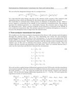
Signal
Top Face
Side sputtering
Ni/Ag/Ni
Polycarbonate
Gap: 2.0
B
A
D
C
y
x
z
43.0
22.0
4.3
6.0 9.0
2.0
7.7
10.0
24.0
Unit: mm
Ground
Ø15
Ø15
Fig. 6. Prototype photo image of the Ni/Ag/Ni thin film internal antenna by sputter –
deposited
Fig. 7. SEM images of the Ni/Ag/Ni thin films by sputter-deposited. (a) primary growth
image of the Ni surface with × 25,000, 30.0kV and 6.0um, (b) redundancy growth image of
the Ag surface with × 10,000, 30.0kV and 8.8um, (c) last growth image of the Ni surface with
× 1,000, 30.0kV and 8.8um, (d) Interfacial tension image of the Ni/Ag/Ni thin film by
sputter-deposited
Advanced Trends in Wireless Communications
446
Figure 8 shows of the material spectrums distribution image for the Ni/Ag/Ni thin film
radiator. Figure 8 (a) shows the properties of materials distribution result at Ni surface layer
from 0keV to 12keV, the Ni material spread distributions are each 0.743 keV, 0.762 keV,
0.851 keV, 7.478 keV, and 8.265 keV. Figure 8 (b) shows of the Ag material distribution
properties curve on Ni material surface also the Ag material spread distributions are each
2.643 keV, 2.806 keV, 2.984 keV, and 3.151 keV. The Ni material characteristic of peak-to-
peak is 0.743 keV and the Ag material peak-to-peak is 2.634 keV. Figure 8 (c) shows of the Ni
surface (Ni/Ag/Ni) spectra image and of material properties spread spectrum for both
materials (Ag and Ni).
Ni material peak
Ni 0.743 keV
Ni 0.762 keV
Ni 0.851 keV
Ni 7.478 keV
Ni 8.265 keV
Ni/Ag material peak
Ag 2.643 keV
Ag 2.806 keV
Ag 2.984 keV
Ag 3.151 keV
Ni: None
(a) (b)
Ni/Ag/Ni material peak
Ni 0.743 keV
Ni 0.762 keV
Ni 0.851 keV
Ni 7.478 keV
Ni 8.265 keV
Ag 2.643 keV
Ag 2.806 keV
Ag 2.984 keV
Ag 3.151 keV
(c)
Fig. 8. The Energy-dispersive X-ray spectroscopy pattern images for Ni surface and Ag
surface on Ni/Ag/Ni thin film. (a) Spectra image of Ni surface, (b) spectra image of Ni/Ag,
(c) spectra image of Ni/Ag/Ni surface
Fabrication and Characterizations of Multi-Layer Thin Film Internal Antenna
for Wireless Communication
447
2.4 Characteristics of SWR for the Ni/Ag/Ni thin film internal antenna by sputter-
deposited
Figure 9 shows the measurement results of the SWR for prototyped sputter-deposit internal
antenna versus optimized with the Ni/Ag/Ni thin film. The operated frequency range is
800 MHz to 2.0 GHz measurement used by Agilent Network Analyzer (E5071B). Figure 9
shows SWR characteristics of the prototyped Ni/Ag/Ni thin film internal antenna and
optimized one. The SWR results of prototyped one are indicates each 3.13, 3.17, 3.09 and
2.22 at 824 MHz, 960 MHz, 1710 MHz and 1990 MHz. On the contrary, the case of the
optimized Ni/Ag/Ni thin film radiator’s SWRs are each 2.18, 2.52, 3.55, and 2.27 at 824
MHz, 960 MHz, 1710 MHz and 1990 MHz, respectively which is fine-tuned with phi type
matching network through Agilent ADS simulation. Figure 10 shows of the prototyped
Ni/Ag/Ni thin film internal antenna and optimized Ni/Ag/Ni thin film internal
antennas S
11
characteristics. In Figure 10 show prototyped thin film S
11
result. The
measured of S
11
are each -5.74 dB and -5.67 dB at 824 MHz and 960 MHz also -5.82 dB and
-8.44 dB at 1710 MHz to 1990 MHz. On the contrary, optimized internal antenna results
marks -8.60 dB, -7.26 dB, -5.01 dB, and -8.22 dB at 824 MHz, 960 MHz, 1710 MHz and 1990
MHz, respectively.
1.01.21.41.61.80.8 2.0
2
4
6
8
10
12
0
14
freq, GHz
VSWR1
VSWR2
GSM850
GPS
DCS
PCS
Measured value (origin Ant. with
sputtered internal antenna)
EGSM
Measured value (After fine tuning Ant. with
sputtered internal antenna)
1.01.21.41.61.80.8 2.0
2
4
6
8
10
12
0
14
freq, GHz
VSWR1
VSWR2
GSM850
GPS
DCS
PCS
Measured value (origin Ant. with
sputtered internal antenna)
EGSM
Measured value (After fine tuning Ant. with
sputtered internal antenna)
Fig. 9. Measured SWR result comparison the sputter-deposit internal antenna versus after
fine tuning the Ni/Ag/Ni thin film internal antenna
Advanced Trends in Wireless Communications
448
1.0 1.2 1.4 1.6 1.80.8 2.0
-16
-14
-12
-10
-8
-6
-4
-2
-18
0
freq, GHz
dB(S(1,1))
dB(S(2,2))
GSM850
GPS
DCS
PCS
Measured value (origin Ant. with
sputtered internal antenna)
Measured value (After fine tuning Ant. with
sputtered internal antenna)
EGSM
1.0 1.2 1.4 1.6 1.80.8 2.0
-16
-14
-12
-10
-8
-6
-4
-2
-18
0
freq, GHz
dB(S(1,1))
dB(S(2,2))
GSM850
GPS
DCS
PCS
Measured value (origin Ant. with
sputtered internal antenna)
Measured value (After fine tuning Ant. with
sputtered internal antenna)
EGSM
Fig. 10. Measured S
11
result comparison the sputter-deposit internal antenna versus after
fine tuning the Ni/Ag/Ni thin film internal antenna
2.5 Characteristics of current distribution for the Ni/Ag/Ni thin film internal antenna by
sputter-deposited
In this experiment describes effect of current distribution for the Ni/Ag/Ni thin film
internal antenna. The Ni/Ag/Ni thin film internal antenna solution is efficient rate in each
frequency ranges. The prototyped Ni/Ag/Ni thin film internal antenna’s overall size is 43.0
× 24.0 × 0.0015mm
3
. The simulation result shows 131A/m and 44.5A/m at 870MHz and
1990MHz. Figure 11 and Figure 12 shows the optimized current distribution results for the
Ni/Ag/Ni sputter-deposit internal antenna. The measured current distribution ratio of
optimized Ni/Ag/Ni sputter-deposit internal antenna is better off than prototype internal
antenna. Figure 13 and Figure 14 shows efficiency distribution image for the optimized
Ni/Ag/Ni sputter-deposit internal antenna at 870MHz and 1990MHz, total efficiency result
are 47% and 55% in par field condition, respectively.
Figure 15 through Figure 18 shows of the 3D far-field (theta and phi) simulated radiation
pattern results for the optimized sputter-deposit internal antenna in free space and SAM
condition. The simulated frequency range is 870MHz and 1990MHz used by SEMCAD
computing program. The results of measured 3D far-field TRP and TIS shows good
performance in free space and SAM condition also measured directivity and gains as well as
total efficiency rate are agreed well at 870MHz to 1990MHz. The measured of TRP
simulation results are each 28.84dBm and 28.30dBm at 870MHz and 1990MHz with SAM
condition. Also, measured of TIS simulation results are -101.85dBm and -101.31dBm at
870MHz and 1990MHz with SAM condition. The simulated results listed in Table 2 at free
space and SAM condition. The measured two kinds of the experiment is significant meaning
which is consumer related aspect.
Fabrication and Characterizations of Multi-Layer Thin Film Internal Antenna
for Wireless Communication
449
Fig. 11. Optimized current distribution image of the pilot radiator with Ni/Ag/Ni thin film
internal antenna handset at 870MHz with CST program (Computer Simulation Technology)
Fig. 12. Optimized current distribution image of the pilot radiator with Ni/Ag/Ni thin film
internal antenna handset at 1990MHz with CST program
Fig. 13. Optimized total power distribute efficiency image of the pilot radiator with
Ni/Ag/Ni thin film internal antenna handset at 870MHz (with CST program)
Advanced Trends in Wireless Communications
450
Fig. 14. Optimized total power distribute efficiency image of the pilot radiator with
Ni/Ag/Ni thin film internal antenna handset at 1990MHz (with CST program)
Fig. 15. Optimized 3D Far-field (θ , φ) radiation pattern image of the pilot radiator with
Ni/Ag/Ni thin film internal antenna handset at 870MHz free space condition (with
SEMCAD program)
Obviously say, the simulated and measured results of the proposed Ni/Ag/Ni sputter-
deposit internal antenna show good agreement with each other in free space and SAM
condition.
φ
x
y
Fabrication and Characterizations of Multi-Layer Thin Film Internal Antenna
for Wireless Communication
451
Fig. 16. Optimized 3D Far-field (θ , φ) radiation pattern image of the pilot radiator with
Ni/Ag/Ni thin film internal antenna handset at 1990MHz free space condition (with
SEMCAD program)
Fig. 17. Optimized 3D Far-field (θ , φ) radiation pattern image of the pilot radiator with
Ni/Ag/Ni thin film internal antenna handset at 870MHz SAM condition (with SEMCAD
program)
φ
x
y
φ
θ
Advanced Trends in Wireless Communications
452
Fig. 18. Optimized 3D Far-field (θ , φ) radiation pattern image of the pilot radiator with
Ni/Ag/Ni thin film internal antenna handset at 1990MHz SAM condition (with SEMCAD
program)
Free space SAM
3-D Far Field
(θ , φ)
870MHz 1990MHz 870MHz 1990MHz
Total Radiated Power()
rad
P
1.687W
(32.27dBm)
0.853W
(29.31dBm)
0.767W
(28.84dBm)
0.676W
(28.30dBm)
Total Isotropic Sensitivity()
TIS
P
-105.28 dBm -102.32dBm -101.85dBm -101.31dBm
Directivity ()
i
dB
2.12 4.90 3.96 6.88
Gain ()
i
dB
1.54 1.29 -0.17 2.20
Total Efficiency ()
total
η
0.84 0.42 0.38 0.34
Table 2. Comparisons of 3D Far-field (θ , φ) radiation pattern for the Ni/Ag/Ni sputter-
deposit internal antenna handset at free space and SAM condition each frequencies (f = 870
MHz, 1990 MHz)
2.5 Characteristics of antenna performance with SAM condition
This section describes the radiation pattern characteristics of the carrier-based internal
antenna and the sputter-deposit internal antenna. Figure 19 shows of radiation pattern
results in SAM condition. The measured radiation pattern experiment is very significant for
antenna performance aspects. At the same times this method can verify the close to real
φ
θ
Fabrication and Characterizations of Multi-Layer Thin Film Internal Antenna
for Wireless Communication
453
human effect. Figure 19 shows of the measured data of peak and average gain for carrier-
based internal antenna radiation patterns, Figure 19 (a) shows the E1-plane (y-z plane)
measured result, Figure 19 (b) shows E2-plane (x-z plane) and Figure 19 (c) shows H-plane
(x-y plane) characteristics at 869MHz and 1930MHz, the carrier-based internal antennas
same to measured in an anechoic chamber complied with CTIA (CTIA Certification, 2005).
(a) (b)
(c)
Fig. 19. Measured radiation pattern of E-plane and H-plane for the sputter-deposit
Ni/Ag/Ni internal antenna handset at resonance (f = 869 MHz, 1930 MHz) (a) E1-plane, (b)
E2-plane, (c) H-plane
The measured results of peak gain each E1, E2, and H-plane are listed in Table 3. Shows of
the experiment result, the measured E1-plane (y-z) average radiation gains are each -6.05dBi
and -5.55dBi at 869MHz and 1990MHz and then measured E2-planes (x-z) average radiation
gains indicates -9.20dBi and -5.45dBi at 869MHz and 1930MHz also, the measured H-plane
Advanced Trends in Wireless Communications
454
(x-y) average radiation gains are each -9.20dBi and -5.34dBi at 869MHz and 1930MHz,
respectively. Furthermore, measured E1-plane (y-z) peak radiation gain results are -
5.92dBi (165 degree) and -2.49dBi (335 degree) at 869MHz and 1990MHz and then the
measured E2-planes (x-z) peak radiation gains are -5.89dBi (355 degree) and -1.44dBi (345
degree) at 869MHz and 1930MHz also, the measured H-plane (x-y) peak radiation gains
indicates -5.37dBi (250 degree) and -2.36dBi (30 degree) at 869MHz and 1930MHz,
respectively.
Consequently, two kinds of internal antenna radiation pattern show good agreement as well
as meet for CTIA regulation. Especially, the proposed Ni/Ag/Ni thin film internal antenna
result shows come to good basis on experiment. Therefore, in this research is enormous
benefit such as extended to antenna carrier volume and adapted diversity topology for next
generation wireless mobile antenna solution also cost effective.
Frequency E1-plane (y-z) E2-plane (x-z) H-plane (x-y)
Gain Average
869 MHz -6.05 dBi -9.20 dBi -5.97 dBi
1930 MHz -5.55 dBi -5.45 dBi -5.34 dBi
Gain Peak
869 MHz -5.92 dBi, 5 deg -5.89 dBi, 355 deg -5.37 dBi, 250 deg
1930 MHz -2.49 dBi, 165 deg -1.44 dBi, 345 deg -2.36 dBi, 30 deg
Gain min
869 MHz -23.61 dBi, 85 deg -42.88 dBi, 270 deg -6.87 dBi, 85 deg
1930 MHz -35.00 dBi, 325 deg -21.54 dBi, 285 deg -13.70 dBi,245 deg
Table 3. Measured E-plane and H-plane radiation pattern for the Ni/Ag/Ni sputter-deposit
PIFA antenna handset at resonance (f = 869 MHz, 1930 MHz), E1-plane (y-z plane), E2-plane
(x-z plane), and H-plane (x-y plane)
2.6 Characteristics of field test
In this section, outlines evaluating for wireless handset performance through the analysis
of voice quality and handset sensitivity measurements. In particular, this experiment is
considered collected voice quality measurements in live-network test beds. This method is
close to user experience. In this experiment discusses the collected voice quality
measurement, handset sensitivity, and field trial performance. Figure 20 describes a
sound source of speak British English and portion of speak British English with metrico
field trial system. It means that measurements made using non-speech signals, such as
tones or white noise, are unrepresentative and misleading. Metrico field experiments
operate with 5 sec for each of two talkers (one male, one female), 10 sec in total (Metrico
Muse system). Therefore, these sections discuss the field trial results between the carrier-
based internal antenna handset and the proposed sputter-deposit internal antenna
handset.
Fabrication and Characterizations of Multi-Layer Thin Film Internal Antenna
for Wireless Communication
455
The experiments methods for data generation consist of the usage of mobile phones while
make a call inside cars. On the contrary, communicated base station located in possible to
make a connection. The metrico field trial system can verify the communication error and
data generation interact with mobile phone, which is uplink and downlink paths. This
experiment test bed is used on country lanes in Figure 21. To figure out how many times
disconnect a call and the variation of electric field strength in worst GSM field area is the
purpose of this experiment
Fig. 20. Portion of the speak British English with metrico field trial system; 5 sec for each of
two talkers (one male, one female), 10 sec in total
Downlink MOS Uplink MOS
Carrier-based
Internal
Antenna
Handset
Sputter-deposit
Internal
Antenna
Handset
Carrier-based
Internal
Antenna
Handset
Sputter-deposit
Internal Antenna
Handset
Average 3.64 3.62 3.49 3.51
Standard Deviation 0.40 0.41 0.28 0.32
Maximum Score 4.10 4.07 3.92 3.94
Count 202 202 202 202
% MOS gather than 3.2 88% 87% 88% 85%
% MOS less than 3 9% 9% 7% 10%
% MOS less than 2.3 2% 1% 0% 1%
Table 4. Comparison of MOS distribution result the carrier-based internal antenna handset
and the sputter-deposit based internal antenna handset at Maryland Baltimore Howard area
(2G GSM network)
Advanced Trends in Wireless Communications
456
Fig. 21. Photo image of the 2G (GSM network) field trial route and the handover area
information in USA (Microsoft Virtual Earth)
A
Total: 13.39 miles
1. A-B: 0.85miles
2. B-C: 6.82miles
3. C-D: 2.36miles
4. D-A: 3.36miles
B
D
C
Handover
Handover
Fabrication and Characterizations of Multi-Layer Thin Film Internal Antenna
for Wireless Communication
457
Downlink MOS Dis tribution
-5%
0%
5%
10%
15%
20%
25%
30%
35%
40%
MOS Range
Percentage of Values in MOS Range
Carrier based internal antenna
Sputter-deposited internal antenna
Carrier based internal antenna
0% 5% 4% 35% 23% 9% 5% 0% 3% 2% 1% 2% 1% 3% 0% 0% 1% 1% 0% 0% 0% 1% 0%
Sputter-deposited internal antenna
0%10%2%34%19%7%1%5% 3%4%3% 0%0%1%1%3%1%0%0%0%0%0%1%
>4.1
4.0-
4.1
3.9-
4.0
3.9-
3.8
3.8-
3.7
3.7-
3.6
3.6-
3.5
3.5-
3.4
3.4-
3.3
3.3-
3.2
3.2-
3.1
3.1-
3.0
3.0-
2.9
2.9-
2.8
2.8-
2.7
2.7-
2.6
2.6-
2.5
2.5-
2.4
2.4-
2.3
2.3-
2.2
2.2-
2.1
2.1-
2.0
<2.0
(a)
Uplink MOS Distribution
-5%
0%
5%
10%
15%
20%
25%
30%
35%
40%
MOS Range
Percentage of Values in MOS Range
Carrier based internal antenna
Sputter-deposited internal antenna
Carrier bas ed internal antenna
0% 0% 0% 3% 2% 34% 32% 6% 2% 7% 3% 1% 1% 1% 1% 1% 0% 1% 0% 0% 0% 0% 0%
Sputter-deposited internal antenna
0% 0% 5% 6% 4% 36% 22% 5% 4% 2% 3% 2% 3% 2% 2% 1% 0% 0% 0% 0% 0% 0% 0%
>4.1
4.0-
4.1
3.9-
4.0
3.9-
3.8
3.8-
3.7
3.7-
3.6
3.6-
3.5
3.5-
3.4
3.4-
3.3
3.3-
3.2
3.2-
3.1
3.1-
3.0
3.0-
2.9
2.9-
2.8
2.8-
2.7
2.7-
2.6
2.6-
2.5
2.5-
2.4
2.4-
2.3
2.3-
2.2
2.2-
2.1
2.1-
2.0
<2.0
(b)
Fig. 22. Comparison of MOS distribution result the carrier-based internal antenna handset
with sputter-deposit based internal antenna handset at Maryland Baltimore in USA (2G
GSM network)
Advanced Trends in Wireless Communications
458
Figure 22 shows MOS distribution profile between the carrier-based internal antenna
handset and the proposed sputter-deposit internal antenna handset in Maryland Baltimore
Howard area. Computed the total distance is 13.39miles, Serving cell and neighbor cell
network indicates each 133, 142, 145, 146 channel in GSM850 band also indicates 636, 630,
670 channel in GSM 1900 at start place, until now measured Rx sensitivity range is -80dBm
to -103dBm around A boundary. Also bring about network handover at C to D area and D
to A area in Figure 21. Figure 23 shows the real-log data about D to A handover area. Table
4 shows MOS distribution result comparison between the carrier-based internal antenna
handset and the proposed sputter-deposit internal antenna handset. As a result, two kinds
of handsets average MOS score marks over 3.0. Namely, carrier-based internal antenna
handset and the sputter-deposit internal antenna handset is “fair” and “Good” performance
in Uplink and Downlink paths. Because of Metrico field trial system basis on ITU defined
theory, in other words, ITU defined voice quality ratio at five-point scale each called the
mean opinion score (MOS) step, where 1 is poor and 5 is excellent quality. Therefore, the
proposed sputter-deposit internal antenna handset shows good performance in the GSM
network (ITU-T Rec., 2001).
Fig. 23. Field trial log information of the GSM 2G network serving and Neighbor cell nearby
Old Frederick Rd 99 and Woodstock Rd subway 125 junctions
3. Conclusion
This chapter fabricated and estimated of the novel Ni/Ag/Ni thin film internal antenna.
Also, experiment characteristics of SWR and efficiency aspect for the proposed Ni/Ag/Ni
thin film solution. The experiment Ni/Ag/Ni thin film internal antennas overall size is 43.0
× 24.0 × 0.0015mm
3
without feeding mechanism. As the demonstrated results, the proposed
Ni/Ag/Ni thin film internal antenna has dual resonances in frequency which is suitable for
a quad-band mobile communication system. Furthermore, the proposed Ni/Ag/Ni sputter-
deposit planar inverted-F antenna occupies attractive size in volume. Briefly speaking of the
Fabrication and Characterizations of Multi-Layer Thin Film Internal Antenna
for Wireless Communication
459
this experiment results, in this chapter reviewed fabrication process and characteristics for
the Ni/Ag/Ni thin film internal antenna by sputter-deposited on polycarbonate substrate
with 1.5um thickness, which is layers sputtered each 3,000Å, 8,000Å and 4,000Å,
respectively. As a result, this solution is proven out last layer has characteristics of both
materials Ag and Ni in distribution material spread spectrum. Moreover, the optimized
SWRs and gain characteristics of radiation patterns are suitable for quad-band antenna.
Also, this experiment verified comparison with carrier-based internal antenna having 40.4 ×
19.2 × 6.25mm
3
volumes as well as this research performed current distribution and
efficiency simulation used by CST and SEMCAD computing program.
The objective of this research is to perform an interaction with human head and field
experiments used the carrier-based internal antenna and the sputter-deposit Ni/Ag/Ni thin
film internal antenna. This research has the previous test result of radiation pattern
characteristics with SAM condition from 824MHz to 1990MHz each E1, E2 and H plane on
both side antennas. Also, this research is investigated for field trial effect comparing with
reference handset including carrier-based internal antenna handset and the proposed
sputter-deposit internal antenna handset having the Ni/Ag/Ni thin films at each 2G, 3G,
and DOOC live-network test beds. As a consequence, the proposed sputter-deposit internal
antenna handset obtained over 3.0 MOS score in the GSM network also, over 3.5 MOS score
at WCDMA live-network at Baltimore Maryland in USA. The real field test result shows that
the performance of the proposed Ni/Ag/Ni sputter-deposit internal antenna is almost same
as carrier-based internal antenna, and especially at the 3G field, the strength of electric field
is very stable. And then, this study found that the evidence converging to support the
experiments from interaction with human head effect and field trial results (2G, 3G and
DOOC field trial)
To conclude, this research is very attractive for adapting to wireless applications such as
portable antenna, MediaFLO antenna, and so on. Furthermore, the Ni/Ag/Ni thin film
internal antenna radiation performances show good agreement as well as meet for CTIA
regulation and field test performances. Therefore, I firmly hold a view that the sputter-
deposit internal antennas exercise is a far-reaching positive influence upon wireless mobile
systems and embed modem or device application having several GHz for next generation
mobile solution that is also cost effective.
4. References
F. Adachi, M. Sawahashi, and H. Suda, Wideband DS-CDMA for Next Generation Mobile
Communications Systems, IEEE Communications Magazine, Vol. 36, pp. 56-69, 1998.
K. Hirasawa and M. Haneishi, Analysis, Design, and Measurement of Small and Low Profile
Antennas, Artech House, ISBN 0-89006-486-5, 1991.
W. L. Stutzman and G. A. Thiele, Antenna Theory and Design, John Willy & Sons Inc. press,
1998.
D. Yuepeng, The Film Sputtering of Gadolinium and Chromium-doped Yttrium Aluminum
Garnet, Ph.D Dissertation, The University of Tennessee, Knoxville, pp.1-14, 2005.
G. C. Stutzin, K. Rozsa, and A. Gallangher, Vacuum, Surface, and Films, Journal of Vacuum
Science & Technology, Vol. 11, p 647, 1993.
CTIA Certification, Test Plan for Mobile Station over the Air Performance, Revision 2.1,
CTIA, p.142, 2005.
Advanced Trends in Wireless Communications
460
C. T. P. Song, P. S. Hall, P. S. Ghafouri-Shiraz, and D. Wake, Triple Band Planar Inverted F
Antennas for Handheld Devices, Electronics Lett., Vol.36, p.112, 2000.
ITU-T Rec., An Objective Method for End-to-end Speech Quality Assessment of
Narrowband Telephone Networks and Speech Codecs, International
Telecommunication Union, Geneva, Switzland, P.862, 2001.
Metrico Muse system,
Microsoft Virtual Earth,
24
Design of CMOS Integrated Q-enhanced
RF Filters for Multi-Band/Mode
Wireless Applications
Gao Zhiqiang, Associate Professor
Department of microelectronics of Harbin Institute of Technology
China
Section I: Wideband reconfigurable CMOS Gm-C filter for wireless
applications
1. Introduction
Recent developments in portable applications and systems have lead to a significant in
wireless standards. Therefore, cost efficiency of CMOS technology implementation has been
greatly enhanced with the emergence of multi-mode wireless applications. Now multi-
mode/multi-band receivers are designed based on the scheme of reuse
[1]-[3]
. They avoid
using multiple chipsets and can be made tunable which makes them more efficient in term
of area and power consumptions. In a flexible receiver front-end, analog baseband filtering
is a key task as it is used to select the required information under desired channel
bandwidth. A large tuning range of the band-pass filter should be required for various
wireless applications.
To meet different specifications for the desired channel in multimode receivers, there has
been a tremendous amount of research [1-6] effort aimed at improving the performance of
integrated reconfigurable continuous-time (CT) filters in recent years. However, due to the
open-loop operation nature, Gm-C filters generally use operational transconductance
amplifier (OTA) driving a capacitor load at the cost of moderate linearity, sensitivity to
parasitics. Moreover, the major disadvantage of OTA is the large distortion caused by the
nonlinear behavior of the transistors involved. To enhance the linearity of the OTA and
avoid potential stability problems, an approach to linear Gm-C integrators with inherent
CMFB is developed based on the techniques of the cross-coupled differential pairs and
source degeneration with passive resistors. In Section 2, the high linear transconductor Gm
is presented. The design of the Chebyshev bandpass filter is discussed, as such the
simulated results of the bandpass filter are given in Section 3. The conclusion is given in
Section 4.
2. The linearized techniques of transconductors
The transconductor in CMOS process is required for wideband reconfigurable Gm-C filter.
Thus, the following section discusses the reported basic linearity technique in CMOS
Advanced Trends in Wireless Communications
462
process. The transconductor linearity techniques can be broadly classified into three types:
(a) source degeneration (b) cross coupling (c) active biasing.
2.1 Source degeneration
Figure 1 shows circuit implementation of the source degeneration technology. The feedback
equivalent resistance R (or M3, M4) is called source degeneration resistor, and differential
pair M1, M2 and source degeneration resistors consist of the structure of source
degeneration. The output current of the structure is related to the input voltage by the
following equation
2
12
21
2
−
=−=− −
dO
OD D dO SS
SS
K(V I R)
II I (VIR)KI
I
(2.1)
Where
0
1
2
=μ
ox
W
KC
L
, I
SS
is tail current source of the transconductor as shown in Figure 1,
and the nonlinearity term of (2.2) is
−
dO
VIR.
Fig. 1. The typical source-degeneration structure of transconductor
The transconductance Gm of source–degeneration structure can be about expressed as
1
≈
+
m
m
g
Gm
gR
(2.2)
When the resistance is much greater than 1/gm, the transconductance Gm≈1/R. However,
this is traded-off with the noise and power consumption. In CMOS process, high quality
passive resistance is achieved difficultly.
2.2 Cross coupling
A simple differential pair can cancel out the even order harmonics of distortion of
transconductor output current. The remaining odd order harmonics can be cancelled out by
Design of CMOS Integrated Q-enhanced RF Filters
for Multi-Band/Mode Wireless Applications
463
two cross-coupling differential pairs with the same distortion but with different gm values.
The circuit is shown in Figure 2.
Fig. 2. The transconductor with differential cross-coupled pairs
The 3
rd
order harmonic is the main concern since it is now the most significant distortion.
From Eq. (2-3), the 3
rd
order harmonic distortion (HD3) of output current can be obtained as:
3
2
3
3
22
=
d
SS
K
HD V
I
(2.3)
Since HD3 depends on the ratio of K
3/2
and Iss
1/2
only, the distortion can be cancelled by
connecting two differential pairs M1, M2 in parallel with M3, M4 as shown in Figure 2. The
transconductor parameter K
3,4
and K
1,2
are related to I
SS2
and I
SS1
as follows:
()
()
3
3
34 34
2
12 1
12
⎛⎞
⎛⎞
⎜⎟
==
⎜⎟
⎜⎟
⎜⎟
⎝⎠
⎝⎠
,,
SS
,SS
,
WL
K
I
KWLI
(2.4)
The corresponding effective gm is then given by:
2
2
3
34
2
12 12
12 1
11
⎛⎞
⎛⎞
=− =−
⎜⎟
⎜⎟
⎜⎟
⎝⎠
⎝⎠
,
SS
meff m, m,
,SS
K
I
gg[ ]g[ ]
KI
(2.5)
According to equation (2.5), when I
SS2
«I
SS1
, the transconductance is approximated as
linearity. But the noise performance is worse than that of a simple differential pair because 2
differential pairs are connected. However, the noise is not doubled because K
3,4
< K
1,2
.
2.3 Active biasing
The idea of active biasing is to make the biasing current compensate for the non-linear term:
2
2
=+
d
SS DC
KV
II
(2.6)
Advanced Trends in Wireless Communications
464
Where I
DC
is the DC bias current, and V
d
is input differential signal. Now the bias Iss
supplies I
DC
when V
d
= 0 for the static bias. When there is a signal, an additional bias current
KV
d
/2 will compensate for the drop of the gm. This can be verified by inserting the new Iss
into Eq. (2.7):
2
12
2+= −
DD gsth
II K(VV) (2.7)
Fig. 3. The transconductor with active-biasing differential pair
In this design, all transistors are matched except M5-M8. For this cascode circuit, when there
is an input signal, the same amplitude appears at the drains of M1 and M2 because the
loading is 1/gm
3,4
and gm
3,4
=gm
1,2
. The capacitance at that node and the loss of the level
shifter M5-M8 are ignored. Both gates of M
b1
and M
b2
sense the differential voltage. Because
the drains of M
b1
and M
b2
are connected together, a bias current is obtained as in Eqs. (2-26).
The required active biasing is then established. But in the common-mode sense, now the
conductance of M
b1
and M
b2
increases in phase with the input signal. This is a kind of feed-
forward and thus causes a boost-up of the common-mode gain. As a result, CMRR drops
and common-mode instability will be resulted.
2.4 The design of high linear transcoductor
The OTA is based on the Gilbert multiplier, which uses the two cross-coupled differential
pairs (M1 - M2, M3-M4) as the input stage to reduce the nonlinearities as shown in Figure 6.
Thank to mismatching of passive resistor in CMOS process, active source-degeneration
resistor M
R1
and M
R2
is perfect choice. For this OTA structure, all transistors operate in the
saturation region except for the transistors M
R1
and M
R2
. The MOS transistor is
approximated as
1
≈−−
RR th CMS
eq
K(V V V )
R
(2.8)
Design of CMOS Integrated Q-enhanced RF Filters
for Multi-Band/Mode Wireless Applications
465
Where K
R
is relative to MOS process parameter, V
R1, 2
is control voltage of source
degeneration resistor, and V
CMS
is common-mode voltage of tail current source. The output
current of the transconductance is
12 13 24 14 23
22
12
12
21 21
22
=
−= − − − = + − +
⎛⎞ ⎛⎞
=−−−
⎜⎟ ⎜⎟
⎝⎠ ⎝⎠
OO O d d d d d d d d
dd
DC d DC d
dsat dsat
I I I (I I)(I I)(I I)(I I)
VV
KI V KI V
VV
(2.9)
Where V
d
is input differential voltage, I
DC1
, I
DC2
is drain terminal current M
b1
-M
b4
respectively. V
dsat1
, V
dsat2
is source-drain overdrive voltage M
b1
-M
b4
respectively. Expanding
(2.9) in the Taylor series and considering the first three terms only, the even terms for
differential is neglected, and (2.10) becomes
3
12
12 1 2
22
12
1
8
=−≈ − − −
mm
OO O m md d
dsat dsat
gg
II I (g g)V ( )V
VV
(2.10)
Fig. 4. The Gilbert OTA with source degeneration
Taking into account the mobility degradation, equation (2.10) is expressed as
12
12
11 22
3
12
2323
111 222
11
1
81 1
=−≈ −
′′
++
−−
′′
++
mm
OO O d
mm
mm
d
dsat m dsat m
gg
II I ( )V
gR gR
gg
(V
V( gR)V( gR)
(2.11)
where
11 1
θ
′
=+RRR
,
22 2
θ
′
=
+RRR, R
θ1,
R
θ2
are source series resistance of the mobility
degradation,
2
θ
θ
=R
K
, and θ is the mobility reduction coefficient.
Advanced Trends in Wireless Communications
466
In equation (2.11), if the nonlinearity third-order term satisfies
12
2323
111 222
0
11
−
=
′′
++
mm
dsat m dsat m
gg
V( gR)V( gR)
(2.12)
Then the transconductance is expressed as
12
11 22
11
=−
′
′
++
mm
mm
gg
Gm
gR gR
(2.13)
If the condition R
/
»1/g
m
is satisfied, the transconductance can be obtained by
12
11
≈−
′
′
m
G
RR
(2.14)
Figure 5 is overall structure of the high linear transconductor. Figure 6 shows the simulation
of step response of the transconductance. When the dc common-mode voltage is about
1.67V, the transient-time response is less than 60ns, and the variation of common-mode
voltage is less than 15mV. We use 5pF as the loading capacitance to verify the AC response
of the transconductor. The bandwidth of unit gain is about 98MHz, and the phase margin is
about 76 degree as shown in Figure 7.
Fig. 5. The overall structure of high linear transconductor
Design of CMOS Integrated Q-enhanced RF Filters
for Multi-Band/Mode Wireless Applications
467
Fig. 6. Step response of the proposed transconductor
Fig. 7. The response of amplitude and phase for the transconductor
Figure 8 shows the simulated Gm plot with the input voltage. The linear range of the
proposed active degenerative resistance (ADR) Gm of cross-couple differential pair is about
±1V. The linear range is higher than the other Gm of differential cross-coupled pair without
ADR and differential pair with ADR (source degeneration structure as shown in Figure 2).
When the operating frequency is 4MHz, the third-order intermodulation IM3 is -72dB as
shown in Figure 9.
Advanced Trends in Wireless Communications
468
Fig. 8. Simulation of linearity for the three differential linearized transconductor
Fig. 9. Response of third-order intermodulation distortion of the OTA at 4MHz