Advances in Photodiodes Part 9 pptx
Bạn đang xem bản rút gọn của tài liệu. Xem và tải ngay bản đầy đủ của tài liệu tại đây (1.15 MB, 30 trang )
Avalanche Photodiodes in Submicron CMOS Technologies for High-Sensitivity Imaging
229
c. Photon Detection Efficiency (PDE). The PDE is the percentage of incoming photons that
create an output pulse over an incident light bandwidth. The probability of a photon
arrival causing an output pulse is reduced by three main factors: reflectance,
absorption, and self-quenching. Firstly, an incoming photon may be reflected at the
surface of the device or at the interface between the many layers that constitute the
optical stack of the detector. An antireflection top coating should ideally be used to
maximise photon transmission through the optical stack. Secondly, a photon may be
absorbed above the SPAD within the optical stack materials, just at the surface of the
active region, or too deep within the silicon substrate in order to initiate an avalanche.
Thirdly, an avalanche event may be initiated but stall, becoming self quenched. Such an
event may not yield enough potential difference in order to trigger an output pulse.
Self-quenching can be minimised by ensuring a high enough electric field is present, so
as to increase chance of impact ionization taking place.
d. Timing resolution (Jitter). When a SPAD is struck repetitively with a low-jitter, short-
pulsed laser, the position in time of the resulting avalanche breakdown pulses has a
statistical variation. The timing resolution, or ‘jitter’ of the detector is the full-width,
half-maximum (FWHM) measure of this temporal variation. Among the timing
resolution components are the variation caused by the generated carrier transit time
from depletion layer to multiplication region, which is dependent on the depth of
absorption of the incident photon (as a guideline, the transit time at carrier saturation
velocity is 10ps per micron), and, more important, the statistical build up of the
avalanche current itself (Ghioni et al., 1988). This is impacted by the electric field
strength, and so jitter may be minimised by employing high overall bias conditions. In
larger area SPADs, also the timing uncertainty introduced by the avalanche lateral
propagation can be non negligible. The shape of the histogram of avalanche events in
response to a time accurate photon arrival provides information regarding the location
and speed of avalanche build up. A predominantly Gaussian shape indicates that the
bulk of photon initiated avalanches occur in the high field active region of the detector,
whereas the presence of a long tail indicates that part of the avalanche events are
initiated by photon-generated carriers diffusing into the high field region of the detector
after a short delay (in this case the timing response at full-width 100th of maximum is
often reported). Of course the method employed for detecting the onset of an avalanche
event is of high importance, and the readout circuit should be designed to minimize
time walk effects.
e. Dead time (T
D
). The SPAD is not responsive to further incoming photons during the
period comprising the avalanche quenching and the reset of the final bias conditions
(Haitz, 1964). However, in the case of a passively quenched SPAD this is not strictly the
case. As the device is recharged via the quenching resistor (a phase that can last from
several tens to a few hundreds of nanoseconds), it becomes increasingly biased beyond
its breakdown voltage, so that it is able to detect the next photon arrival prior to being
fully reset. This behaviour is coupled with a significant fluctuation in the reset
waveform. Clearly the dead time should be kept as small, and as consistent as possible
in order to achieve the highest possible dynamic range of incident photon flux and least
variation in photon count output to a certain photon arrival rate. In this respect, active
quenching circuits offer the best performance with short and well-defined dead times
and high counting rates. However, short dead times are often accompanied by
enhanced afterpulsing probability due to inadequate trap flushing time.
Advances in Photodiodes
230
f. When dealing with arrays of SPADs, other parameters become significant. Among them
are Fill Factor and Crosstalk. The active area of a SPAD is the central photon-sensitive
portion of the detector. The electric field strength should be consistent across this part
of the structure, so as to yield a homogenous breakdown probability. Zones that exhibit
higher field strength will exhibit locally higher photon detection probability and dark
count compared with the rest of the active area. Such zones should be avoided by
proper design solutions, such as guard rings. The proportion of active region area to
total SPAD area is the Field Factor (FF) and is commonly expressed in percent.
Crosstalk between adjacent SPADs can occur in two ways. Firstly, a photon absorbed
deep in one detector may result in a lateral diffusion of carriers to an adjacent device
where an avalanche can be initiated. Secondly, an avalanche event may result in an
electro-luminescent emission of photons that are then detected by an adjacent detector
(Lacaita et al., 1993a). Electrical and optical crosstalk can be minimised by detector
design introducing proper electro-optical isolation structures, at the expense of a
reduction in the active area (Sciacca et al., 2006).
4. State of the art
4.1 Geiger-mode APD (SPAD)
SPADs can be traced back to the deep planar/reach through structures created in the 1960’s
(McIntyre, 1961; Ruegg, 1967; Haitz, 1963). These large, deep junction devices and their
subsequent developments required high reverse bias voltages and were stand-alone
structures incompatible with other circuit elements. Perkin-Elmer, Rockwell Science Center
and Russian research groups have all since contributed to the development of these devices,
as well captured in (Cova et al., 2004; Renker, 2006).
Apart from III-V devices and silicon reach-through structures (not suited to arrays), that are
not covered in this chapter, the state of the art in modern SPADs may be described in terms
of manufacturing process employed and construction details.
Three main process categories can be distinguished:
i. CMOS compatible, full custom processes, optimized to yield the best possible
performing single detector element (e.g., Lacaita et al., 1989): among the adopted
features are low implant doping concentrations, slow diffusion and annealing steps to
minimise silicon lattice damage, gettering phases and embedded constructions to
improve DCR and crosstalk. These implementations allow for small size arrays (Zappa
et al., 2005; Sciacca et al, 2006), but are not compatible with very large-scale integration
(VLSI) of on chip circuitry.
ii. High voltage CMOS processes: both single detectors and arrays have been implemented
with this approach, together with quench circuitry (Rochas et al., 2003b; Stoppa et al.,
2007) and single channel Time Correlated Single Photon Counting (TCSPC) systems
(Tisa et al., 2007), but the scope for large scale integration is limited.
iii. Standard CMOS processes, without any modifications to the layers normally available
to the designer. While providing great potential for VLSI integration and low cost, thus
enabling new applications, this approach has to cope with the limitations imposed by
the shallow implant depths, high doping concentrations, non optimized optical stacks,
and design rule restrictions in advanced manufacturing processes. For this SPAD
category, examples have been reported featuring: high DCR, even up to 1MHz, most
likely due to tunnelling (Niclass et al., 2006; Gersbach et al., 2008) and/or to crystal
Avalanche Photodiodes in Submicron CMOS Technologies for High-Sensitivity Imaging
231
lattice stress caused by shallow trench isolation process (Finkelstein et al., 2006a); low
PDE (Faramarzpour et al., 2008; Marwick et al., 2008), possibly due to non optimized
optical stack.
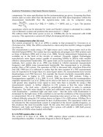
As far as construction details are concerned, the essential features of a SPAD are the method
of formation of the guard ring, the overall shape (i.e. circular, square, others), active area
diameter and the diode junction itself. Today’s nanometer scale processes provide features
such as deep well implants and shallow trench isolation (STI) that may be utilised in
detector design. Additionally some custom processes provide features such as deep trench
isolation, buried implants, and scope for optical stack optimisation.
Even in the very first samples by Haitz and McIntyre, premature edge breakdown was
addressed by an implant positioned at the edge of the junction active region, and hence the
first SPAD guard ring was created. State of the art SPAD constructions can be grouped
according to the method of implementation of the guard ring, as discussed in the following
with the aid of Fig.2 (different constructions are discussed with reference to the different
cross sections shown in Fig.2 from (a) to (f)).
P- substrate
Deep N-well
P-well
P-well
P+
N+N+
anode
cathode
Oxide
hfhf
Contact
(a) (b)
P- substrate
Deep N-well
N-enhance
P+
N+N+
anode
cathode
Oxide
hfhf
Contact
P- substrate
N-well
N-well
N-well
P+
N+N+
anode
cathode
Oxide
hfhf
Contact
(c) (d)
P- substrate
Deep N-well
P+
N+N+
anode
cathode
Oxide
hfhf
Contact
P-well
N- substrate
P- well
P-enhance
N+
anode
cathode
Oxide
hfhf
P+
P+
Buried P+
Contact
(e) (f)
P- substrate
N-well
P+
N+N+
anode
Oxide
hfhf
STI
STI
cathode
Contact
Fig. 2. Cross sections of different SPAD constructions: (a) Diffused Guard Ring; (b)
Enhancement Mode; (c) Merged Implant Guard Ring; (d) Gate Bias and Floating Guard
Ring; (e) Timing Optimised; (f) Shallow Trench Isolation Guard Ring.
a. First introduced for the purposes of investigating microplasmas in p-n junctions under
avalanche conditions (Goetzberger et al., 1963), the diffused guard ring is a lower
doped, deeper implant at the device periphery able to reduce the local electric field
strength. This construction has since been implemented by several research groups
(Cova et al., 1981; Kindt, 1994; Rochas et al., 2002; Niclass et al., 2007). Whilst enabling a
low breakdown voltage using implants that are commonly available in most CMOS
processes, this structure has several limitations. Firstly, when implemented in a modern
CMOS process, the high doping concentration, shallow implants lead to a high electric
field structure, resulting in a high DCR due to tunnelling as predicted by (Haitz, 1965),
confirmed by (Lacaita et al., 1989) and also recently reported in (Niclass et al., 2007).
Advances in Photodiodes
232
Secondly, if long thermal anneal times are employed in relation to the guard ring
implant, the resultant field curvature around this key feature creates a non-uniform,
dome-shaped electric field profile, peaking at the centre of the device. This in turn
implies a breakdown voltage variation across the active region, which strongly affects
the homogeneity of the photon detection efficiency (Ghioni et al., 2007). Thirdly, the
increase of the quasi-neutral field region at the detector edge promotes late diffusion of
minority carriers into the central high-field region, resulting in a long diffusion tail in
the timing resolution characteristic, first reported in (Ghioni et al., 1988), and also
evident in the 130nm implementation of (Niclass et al., 2007). Fourthly, this structure
has a minimum diameter limitation due to merging of the guard ring depletion region
as the active region is reduced, illustrated in (Faramarzpour et al., 2008). This limits the
scalability of the structure for array implementation purposes.
b. The enhancement mode structure, first introduced in the reach-through device of
(Petrillo et al., 1984), was employed in a hybrid diffused guard ring/enhancement
structure (Ghioni et al., 1988), and finally used without the diffused guard ring
structure (Lacaita et al., 1989), relying on a single central active region enhancement
implant (with doping polarities reversed, and embedded in a dual layer P-epitaxial
substrate), which is referred to as a ‘virtual’ guard ring structure. The benefits of this
structure are significant. Firstly, the quasi neutral regions surrounding the guard ring
are removed, and therefore the minority carrier diffusion tail is reduced resulting in
improved timing resolution. Secondly the device does not suffer from depletion region
merging when scaling down the active region diameter, easing the prospect of array
implementations with fine spatial resolution. Both versions were recently repeated but
with dual orientation, range of active areas and active quench circuits in a high voltage
CMOS technology (Pancheri & Stoppa, 2007).
c. An alternative implementation to the diffused guard ring is the merged implant guard
ring, relying on the lateral diffusion of two closely spaced n-well regions, that creates a
localised low-field region, preventing edge breakdown. This technique was
demonstrated using only the standard layers available in a CMOS process (Pauchard et
al., 2000a). Whilst successful with 50Hz DCR, >20% PDE and 50ps timing resolution
being reported (Rochas et al., 2001), this design normally violates the standard design
rules and is difficult to implement. Nevertheless the authors were successful in co-
integrating quenching circuitry and forming small arrays in a 0.8μm CMOS process.
d. Other guard ring ideas are based either on a metal or polysilicon control ‘gate’ biased
appropriately to control the depth of the depletion region in the zone immediately
beneath (Rochas, 2003c), or on a ‘floating guard ring’ implant inserted near the edge of
the active region in order to lower the electric field around the anode periphery (Xiao et
al., 2007). The gate bias method is relatively unproven compared to the more common
guard ring implementations. This is an interesting solution since polysilicon is normally
available to move STI out of the active region. The floating guard ring construction has
parallels with the diffused guard ring construction: it lends itself to be employed with
certain anode implant depths, but requires careful modelling to determine the optimum
layout geometry and can be area inefficient. Implemented in a high voltage technology,
it yielded SPADs with both low DCR and good timing resolution, albeit with a high
breakdown voltage and an off-chip active quench circuit (Xiao et al., 2007).
e. The work of the research group at Politecnico di Milano has prioritised timing
resolution as the key performance metric since early publications utilising the diffused
Avalanche Photodiodes in Submicron CMOS Technologies for High-Sensitivity Imaging
233
guard ring structure (Cova et al., 1981). This focus was maintained in the progression to
devices implemented in a custom epitaxial layer (Ghioni et al., 1988). It was observed
that previously published devices exhibited a long diffusion tail in the timing response.
This was due to minority carriers generated deep in the quasi-neutral regions beneath
the SPAD reaching the depletion layer by diffusion. The single epitaxial layer devices
helped to greatly reduce the diffusion tail by drawing away deep photo-generated
minority carriers via the secondary epitaxial-substrate diode junction. This technique
was taken further in the double-epitaxial structure (Lacaita et al., 1989), and again in the
more complex structure of (Lacaita et al., 1993b). The goal of the ‘double epitaxial’ layer
design was to reduce the thickness of quasi-neutral region below the SPAD in order to
limit the diffusion tail whilst maintaining a high enough electric field to provide fast
response without a high dark count penalty. In the more complex structure of (Lacaita
et al., 1993b) the buried p
+
layer was interrupted underneath the active region in order
to locally fully deplete the main epitaxial layer by reverse biasing the substrate, for the
purpose of eliminating diffusion carriers. Whilst resulting in unprecedented timing
performance (35ps FWHM) with DCR of a few hundred Hertz for a 20μm diameter
structure, the design required full customisation of the manufacturing process, resulting
in limited co-integration capability.
f. The shallow trench guard ring structure was first introduced in 0.18μm CMOS
(Finkelstein et al., 2006a). The main goal of this innovation was to increase FF and allow
fine spatial resolution. The etched, oxide filled trench, that is a feature of deep
submicron processes, is used as a physically blocking guard ring, so containing the high
field zone in the active region. This structure was successful in addressing FF and
potential pixel pitch, although only single devices were reported. However, the
subsequent publication by the same author group (Finkelstein et al., 2006b) revealed a
very high DCR of 1MHz for a small diameter 7μm device. This was possibly caused by
etching-induced crystal lattice defects and charge trapping associated with STI, as well
as band-band tunnelling through the conventional p
+
/n-well diode junction. The same
author group noted in (Hsu et al., 2009) that, despite the high dark count, the timing
resolution characteristic was unspoiled by a diffusion tail due to reduced quasi-neutral
field regions associated with implanted guard rings. Further, it was observed that
increasing the active region diameter had no effect on the 27ps jitter, suggesting that
these structures do not suffer from the lateral avalanche build up uncertainty.
Additionally, the lower junction capacitance yields reduced dead time. There are two
further related publications associated with the use of STI in SPADs. In (Niclass et al.,
2007) the clash of STI with the sensitive active region is avoided by drawing ‘dummy’
polysilicon to move the etched trench to a safe distance away. This was progressed by
(Gersbach et al., 2008), applying a low doped p type implant around the STI interface.
However, the DCR was still around 80kHz for an 8μm active region diameter and 1V of
V
EX
. Timing performance remains acceptable for many applications at ~140ps.
4.2 Linear-mode APD
Commercial linear-mode silicon APDs evolved from the same precursors as SPADs and are
nowadays a mature technology, with outstanding performances in terms of Quantum
Efficiency, Noise Factor and Bandwidth. Several APD products are sold by big companies
(APD producers) for applications requiring low-noise and high speed detection such as laser
Advances in Photodiodes
234
ranging, particle detection, molecule detection, optical communications, etc. Commercial
APDs can have a peak quantum efficiency (QE) exceeding 80%, an excess noise factor F≈M
0.3
for reach-through devices and as low as F≈M
0.17
in the case of Slik
TM
devices fabricated by
EG&G. APDs are commonly used for imaging by mechanical scanning as in the case of laser
range finding or confocal microscopy. Only a few small APD arrays are currently present on
the market, and the maximum number of devices in a single array is currently limited to 64
(8x8 module by RMD). From year 2000, several linear-mode APDs fabricated in CMOS
technologies have appeared in the literature, in various technology nodes. Although their
performance is still far from the one obtained with commercial APDs, their low cost and
possibility of monolithic integration with readout electronics make them appealing in
several application domains. Table 1 lists a selection of CMOS linear-mode APDs so far
presented with some of their performance indicators.
Reference
Node
[μm]
Type
Guard
Ring
V
APD
[V]
QE
[%]
F @ M = 20
Biber 2001 2 p
+
/n-well p-base 42 40 @ 500nm 36000 @ 635nm
Biber 2001 2 n
+
/p-sub n-well 80 75 @ 650nm 1800 @ 635nm
Rochas 2002 0.8 p
+
/n-well p-well 19.5 50 @ 470nm 7 @ 400nm
Stapels 2007 0.8 n
+
/p-sub n-well n.a. >60 @ 700nm 5 @ 470nm
Stapels 2007 0.8 p
+
/n-well p-tub 25 50 @ 550nm 50 @ 470nm
Kim 2008 0.7 n
+
/p-body virtual 11 30 @ 650nm n.a.
Pancheri 2008 0.35 p
+
/n-well p-well 10.8 23 @ 480nm
4.5
6
@
@
380nm
560nm
Table 1. Selected characteristics of CMOS avalanche photodiodes.
Although both p
+
/n-well and n
+
/p-well structures have been presented, the former
structure is preferred if an integrated readout is to be fabricated, because both photodiode
terminal electrodes are available and low voltage circuits can be implemented. However, an
n
+
on p substrate is also feasible, provided it is isolated by means of an n
+
buried layer as in
the case of (Kim et al., 2008). From the point of view of readout noise, an n
+
/p structure is
favored for visible light wavelengths, because the avalanche is electron-initiated. This can be
clearly observed comparing the two structures in (Stapels et al., 2007), where p+/n-well
APD has a noise 10 times higher than n+/p-sub APD. For wavelength shorter than about
400nm, however, an n
+
/p structure can be convenient and has a low noise factor. Passing
from old 2μm technologies to 0.8μm and 0.35μm a positive trend is observed. While the
breakdown voltage is reduced due to the higher doping levels, the noise also becomes
generally lower. One of the reasons is that the ionization coefficient ratio k is closer to unity,
so the noise due to hole initiated avalanche is lower, as can be observed comparing the p+/n
structures in (Biber et al., 2001) and (Stapels et al., 2007). When the doping levels are even
higher, the width of the multiplication region is reduced and standard McIntyre theory is no
longer adequate to describe the avalanche process because of the dead space effect (Hayat et
al., 1992). In this case, the noise factor becomes lower than the one predicted by standard
model both for electron- and hole-initiated avalanche, as observed in (Pancheri et al., 2008).
The positive trend in noise as technology is scaled is, however, accompanied by a reduction
of quantum efficiency due to the reduced absorption region depth and an increase of dark
current due to the contribution of tunneling.
Avalanche Photodiodes in Submicron CMOS Technologies for High-Sensitivity Imaging
235
CMOS APDs are appealing for short distance communications because of their large
bandwidth, exceeding 1GHz. A few successful examples of CMOS APDs in 0.18μm
technology have been reported (Iiyama et al., 2009; Huang et al., 2007; Kang et al., 2007),
with bandwidth figures up to 2.6 GHz and good dark currents, in the nA range.
Nevertheless, the STI used for guard ring implementation can be inefficient for devices with
deeper junctions, resulting in much higher dark currents (Huang et al., 2007).
5. Design and characterization of advanced CMOS avalanche photodiodes
5.1 Geiger-mode APD (SPAD)
(a) High fill factor linear array in a standard 0.35
μ
m CMOS technology
One of the main drawbacks in SPAD arrays presented so far is the low FF, which is in the
order of some percent in the best cases. Even if microlens arrays can be used to improve FF,
their use is subject to a series of technological constraints. Therefore, a reasonably good FF is
important even if the use of optical concentrators is foreseen. There are at least three aspects
that limit the FF: the guard ring, the need to reduce optical cross-talk between neighbouring
pixels and the size of the readout channel, that needs to be much larger than 3T topology
used in standard active pixels.
Fig. 3. Schematic cross section (a) and micrograph (b) of the 4 line SPAD array in 0.35μm
CMOS technology.
We have started tackling this problem with a 4 line array, fabricated in 0.35μm CMOS
technology (Pancheri & Stoppa, 2009). The SPAD array was a 64x4 array, with the 4 devices
in a column sharing the same digital readout channel. In order to improve the FF as much as
possible, SPADs have a square geometry with rounded corners, and have been
implemented in a shared deep n-well. A schematic cross section and a micrograph of the
SPAD array are shown in Fig. 3, and a summary of the main characteristics of the SPADs is
reported in Table 2. A remarkable 34% FF is obtained, which could easily be doubled with
the use of optical concentrators. More than 80% of the SPADs have a dark count rate of
approximately 1kHz, while the remaining 20% have increasingly larger dark counts, a small
percentage exceeding 100 kHz. In addition to the characteristics of single SPADs, in arrays it
is important to consider also PDP non-uniformity and cross talk between pixels. To measure
the first one, we have used a uniform incident light onto the SPAD array by using a
stabilized lamp and an optical diffuser. Light intensity was adjusted to obtain count rates
below 10% of the maximum SPAD count rate, so as to avoid saturation effects. Dark count
rate was subtracted from the recorded counts to take into account only the optically
Advances in Photodiodes
236
generated photons. A non-uniformity lower than 2% was measured at V
ex
= 4V, which is
remarkably good for this kind of device. Cross talk was evaluated by measuring the DCR
variation of a low-DCR SPAD (SL) in the neighborhood of a high-DCR SPAD (SH). When
SH is enabled, a DCR increase of about 1% of the DCR of SH is observed in SL because of
optical cross talk effect. A further effort to increase the FF would increase the cross-talk to
higher levels and have a negative impact for the array performance.
SPAD pitch
26 μm
Fill Factor 34%
Breakdown voltage 31V
Dark count rate @ Room Temperature 1kHz typ.@ V
ex
= 4V
Photon Detection Efficiency
32% @ λ = 450nm
Jitter (FWHM) < 160ps
Afterpulsing rate 6% @ T
D
=200ns
PDP non-uniformity (σ)
< 2% @ V
ex
= 4V
Cross-talk 1%
Table 2. Summary of the main characteristics of SPAD array in 0.35μm CMOS technology.
(b) Low noise SPADs in a 0.13
μ
m imaging CMOS technology
Advanced CMOS technologies have been optimised for high performance transistors,
somewhat contrary to the requirements for low-noise Geiger mode CMOS avalanche
photodiodes. The active region is generally defined between the p
+
source-drain implant
and n-well used to define the bulk of the PMOS transistors. These implants have increased
in doping density and the breakdown mechanism in many structures in 0.18μm and 0.13μm
has switched to tunneling. A further challenge is the presence of shallow trench isolation for
isolation of NMOS transistors from the substrate noise. The first attempts to define a low
DCR SPAD with these technologies, summarized in Section 4, whilst providing good timing
characteristics, still suffered from poor DCR performance.
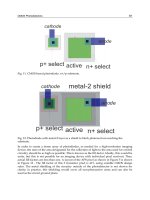
A low-DCR SPAD structure is proposed here which largely attenuates the tunneling
problem of the p
+
/n-well junction by constructing the deep anode from p-well (contacted by
p
+
) in conjunction with the buried n-well. The resulting SPAD represents an alternative to
that reported in (Richardson et al., 2009a), showing outstanding noise performance. A
further novelty in this structure is that the cathode and a new guard ring structure are
formed simultaneously by the use of buried n-well without n-well. This latter technique
requires a drawn p-well blocking layer to inhibit the automatic generation of p-well as the
negative of n-well by the CAD mask Boolean operation. The result is a progressively graded
doping profile in the guard ring region, reducing in concentration near the substrate surface,
as indicated by the shading of the buried n-well zone in Fig. 4(a). This lowers the electric
field at the periphery in comparison to the main p-n junction, as shown in the simulated plot
of Fig. 4(b). The guard ring zone can be kept free of STI by using a poly ring around the
periphery defining a thin oxide region. STI formation is known to introduce defects and
crystal lattice stresses which cause high DCR so it is normally important to move the trench
away from the main diode p-n junction. Finally, the connection to the buried n-well cathode
is implemented by contacting to drawn n
+
and n-well at the outer edge. An attractive
property of this p-well SPAD structure is that it can be implemented in any standard digital
Avalanche Photodiodes in Submicron CMOS Technologies for High-Sensitivity Imaging
237
triple-well CMOS technology. SPADs implemented at older process nodes have required
low-doped wells only found in more costly high voltage technologies.
P-well
Buried N
-
well
p
-
epi substrate
P-epi/Buried N-well guard
(no N-well or P-well
)
N-well
N-well
P+
anode
hf
STI
cathode
N+
N+
P-well
P-well
P-well
Buried N
-
well
p
-
epi substrate
P-epi/Buried N-well guard
(no N-well or P-well
)
N-well
N-well
P+
anode
hf
STI
cathode
N+
N+
P-well
P-well
(a)
(b)
Fig. 4. (a) Cross section of SPAD with retrograde buried n-well cathode and p-well anode;
(b) TCAD simulated electric field distribution (arbitrary scale) showing low field at the
surface increasing at depth with the grading profile of the buried n-well.
-2.50E-10
-2.00E-10
-1.50E-10
-1.00E-10
-5.00E-11
0.00E+00
-15 -14.8 -14.6 -14.4 -14.2 -14 -13.8 -13.6 -13.4 -13.2 -13
-Voltage (V)
Current (A)
A 0deg C
A 15deg C
A 30deg C
10
100
0 200 400 600 800 1000 1200
VEB (mV)
Counts/s
1
10
100
-30 -20 -10 0 10 20 30 40
Te mp (°C)
Counts/s
(a)
(b)
(c)
V
ex
(mV)
Fig. 5. Dark characteristics of the SPAD shown in Fig. 4: (a) Current-Voltage curves; (b)
dark-count rate variation with the excess bias voltage at room temperature; (c) dark count
rate variation with temperature at 0.6V of excess bias voltage.
The characterisation results for an 8μm active diameter SPAD implemented in a 0.13μm CMOS
image sensor process according to the previous construction are now discussed. Figure 5(a)
shows the current-voltage characteristics at three different temperatures: the breakdown knee
occurs at 14.3V, in very close agreement with TCAD simulation (14.4V), and with 83pA of dark
current at breakdown. The variation of the breakdown voltage over temperature is
+3.3mV/°C, indicating that the breakdown mechanism is avalanche (Sze & Ng, 2007). Dark
count rate is reported in Figs. 5(b) and 5(c): the first graph set shows that this detector has a
very low dark count rate with the expected exponential relationship between DCR and excess
bias; the second graph set shows the dark count rate is dominated by thermal carrier
generation at temperatures larger than 5°, the DCR values doubling every 7-8 degrees,
whereas at lower temperatures the reduced slope indicates that tunnelling starts to be non
negligible. Also afterpulsing (not shown) is very low, in the order of 0.02%. This is in line with
the low junction capacitance and photoelectric gain of the considered SPAD.
Advances in Photodiodes
238
Furthermore, the implementation of this detector design in a 32x32 array as part of the
MEGAFRAME Project (MEGAFRAME) provided the opportunity for analysis of DCR
population distribution for 1024 elements, as shown in Fig. 6. The detector had the same
structure as those above but a slightly smaller active region of 7μm diameter. It can be seen
that the population splits roughly into two groups: those with low DCR well below 100Hz,
and those with higher DCR up to 10 kHz. The split ratio is ~80:20. All 1024 SPADs were
functional. The impact on DCR by increased excess bias is evident from the two traces in
Fig. 6.
1.E+00
1.E+01
1.E+02
1.E+03
1.E+04
1.E+05
0% 10% 20% 30% 40% 50% 60% 70% 80% 90% 100
%
% of 1024 Total Population
DCR (Hz)
Cumulative % 0.65V
Cumulative % 0.8V
A
verage: 1.1KHz
Median: 26 Hz
Mode: 20 Hz
Fig. 6. Distribution of dark count rate measured at room temperature in 1024 p-well buried
n-well SPADs of 7μm active region diameter, at two different excess bias voltages.
1
10
100
1000
-1.0
Time (ns)
Counts
-0.8
-0.6
-0.4
-0.2
0.0
0.2
0.4
0.6
0.8
1.0
(b)
Low V
ex
=0.4 V
Mid V
ex
=0.8 V
High V
ex
=1.2 V
0
5
10
15
20
25
30
300
400 500 600 700 800 900 1000 1100
Wavelength (nm)
PDE (%)
Low V
ex
=0.4 V
Mid V
ex
=0.8 V
High V
ex
=1.2 V
(a)
Fig. 7. Electro-optical characteristics of p-well buried n-well SPAD: (a) photon detection
efficiency as a function of wavelength at three different excess bias voltages; (b) time jitter
measured at 470nm wavelength at the same three excess bias voltages.
Fig. 7(a) shows the photon detection efficiency as a function of the wavelength. As expected,
PDE improves with the excess bias voltage at all wavelengths. The deeper p-well junction of
this SPAD results into a peak at around 500nm (green) rather than 450nm of more
conventional p
+
/n-well SPADs. The peak value at 1.2 V excess bias voltage is about 28%.
PDE curves extend beyond 800nm where values ~6% are still observed at higher excess bias.
Avalanche Photodiodes in Submicron CMOS Technologies for High-Sensitivity Imaging
239
The increased response in the near infra-red is useful for several applications, among them
time-of-flight 3D range sensing applications. The perturbations in the response are due to
constructive/destructive interference patterns caused by the dielectric stack above the
detector, which consists of several different materials with varying refractive indices.
Fig. 7(b) shows the timing histograms measured at 470nm wavelength and at the same
excess bias voltages as in Fig. 7(a). Timing resolution is measured as the FWHM of the
distributions. Its values are 199 ps, 192 ps, and 184 ps, at low, mid, and high excess bias
voltage, respectively. A distinct, exponential tail extends for around 1ns after the peak,
evidence of a diffusion related timing delay.
Table 3 shows a performance comparison for SPADs fabricated in 130nm CMOS
technologies. As can be seen, a dramatic improvement in DCR can be achieved by adopting
proper implant layers which lower the electric field, at the expense of a degradation in the
jitter, that however remains good enough for most applications.
Reference This work Gersbach 2009 Niclass 2007
Active area
50.3 μm
2
58 μm
2
53 μm
2
Type p
+
/p-well/buried n-well p
+
/n-well p
+
/n-well
Guard ring
buried n-well
with poly gate
STI with p-type
passivation
p-well/STI
with poly gate
V
BD
14.3V 9.4V 9.7V
DCR 40Hz@V
ex
=1V 670kHz@V
ex
=2V 100kHz@V
ex
=1.7V
PDE 28%@ 500nm 30%@480nm 34%@450nm
Jitter 184ps FWHM 125ps FWHM 144 ps FWHM
Afterpulsing 0.02%@T
D
=100ns <1%@T
D
=180ns n.a.
Table 3. Performance comparison of SPADs made in 130nm CMOS technologies.
5.2 Linear-mode APD
In order to implement APD-based pixels with integrated low-voltage readout channels, both
terminals of the photodiode must be available: one to apply a high voltage and the other to
connect the readout channel. This restricts the choice of the structure to the p+/n-well type
(although also n
+
/floating p-well would be feasible). With technology scaling, the well
doping levels are steadily increasing to allow the integration of smaller-size MOSFETs.
Therefore, APDs fabricated in standard wells would have decreasing breakdown voltages
and increasing tunneling dark currents when migrating the design to more advanced
technology nodes. However, in High Voltage processes, a larger choice of layers with
different doping levels are available, and can be exploited in the realization of APDs, both to
obtain an efficient guard ring and a suitable doping for the multiplication region. The High
Voltage option can then enable the fabrication of APDs also in deep sub-micron
technologies. One key aspect to understand is how the noise factor scales with technology.
Unfortunately, there are only a few examples of noise-characterized CMOS APDs in the
literature, so that only some basic guidelines can be drawn.
Fig. 8 shows the measured noise factor for two p
+
/n-well APDs fabricated in two different
technologies. The APD in Fig.8(a), fabricated in a 0.7μm High Voltage technology, has a
breakdown voltage of 20.8V, and exhibits a low noise factor at low wavelengths because of
electron-initiated avalanche. At higher wavelengths, however, noise increases considerably
due to the hole-initiated avalanche noise. The measurements are in good agreement with
Advances in Photodiodes
240
McIntyre noise theory, considering an ionization ratio k=0.2. The device of Fig. 8(b),
fabricated in 0.35μm CMOS technology, exhibits low noise also in the case of hole-initiated
avalanche. The measured noise does not correspond to the one predicted by McIntyre
theory because of the dead-space effect. This device is therefore more suitable for imaging
applications in the visible spectral region. A further improvement in the noise factor could
be given by n
+
on floating p-well, which would combine the low noise of electron initiated
avalanche with the requirement to access both device terminals. However, for this device
structure, there is no experimental noise characterization available so far.
0
10
20
30
40
50
60
0 10203040
Noise factor, F
Multiplication gain, M
Exp. 650nm
Exp. 380nm
Theory holes
Theory electrons
0
5
10
15
20
25
30
0 1020304050
Noise factor, F
Multiplication gain, M
Exp. 560nm
Exp. 380nm
Theory holes
Theory electrons
(a)
(b)
Fig. 8. Noise factor as a function of multiplication gain at two illumination wavelengths in
two APDs made from: (a) 0.7μm High Voltage and (b) 0.35μm standard CMOS technology.
0.1
1
10
1 10 100
Gain non umiformity, σ
M
[%]
Multiplication Gain, M
Different dies
Same die
Fig. 9. Gain uniformity between 0.35μm CMOS APDs fabricated on the same die and on
different dies in the same production batch.
In the implementation of avalanche photodiode arrays, an important factor to take into
account is gain uniformity. As multiplication gain increases, the voltage range allowing a
tolerable gain variation progressively reduces. Therefore, if small non-uniformities between
different APDs can be corrected via pixel-by-pixel calibration, large non-uniformities are
detrimental to the correct operation of the array. In order to evaluate the uniformity of APDs
made on the same die, a small set of identical APDs, whose characteristics were reported in
Avalanche Photodiodes in Submicron CMOS Technologies for High-Sensitivity Imaging
241
(Pancheri et al., 2008), were fabricated in a 0.35μm CMOS technology. For every APD in the
die and for several dies, the gain was measured as a function of voltage. Gain non-
uniformity, expressed as standard deviation, is reported as a function of average gain in Fig.
9. It can be observed that the gain non-uniformity of APDs fabricated on different dies (in
the same production batch) is 10 times higher than the non-uniformity of gains for APDs
belonging to the same die. In this last case, a non-uniformity better than 1% is achieved for a
gain M=40. This demonstrates the feasibility of linear-mode APD arrays in that specific
technology.
6. Integrated read-out channels for SPADs
Two basic circuit elements are required to read-out a SPAD: i) a quench circuit to detect and
stop the avalanche event, followed by restoration of bias conditions; ii) a buffer to isolate the
SPAD from the capacitance of external processing electronics. The integration of more
complex processing and support circuits such as time-to-digital conversion, gated ripple
counters and charge pumps is the subject of much recent research (Niclass et al., 2008;
Richardson et al., 2009b; Guerrieri et al., 2010). However, as the main properties of the
optical system are set by the choice of quench circuit and associated biasing arrangement for
the SPAD we will focus on these aspects in more detail.
(a) SPAD Orientation Options
Since a SPAD is a two terminal diode, operated at an excess bias potential beyond its
breakdown voltage, it may be oriented in two ways; either with a negative potential on the
anode, or positive on the cathode. As previously discussed, it is desirable to minimise
detector dead time and charge flow quantity during an avalanche event. The optimal
connectivity to permit this depends on the parasitic capacitances which are specific to the
diode construction which has been implemented.
To illustrate this point, two possible passive quench configurations are shown in Fig. 10 for
a SPAD implemented within a deep n-well, p-substrate technology such as that of
(Pauchard et al., 2000b ) Fig. 10(a) shows a large negative voltage applied to the anode, with
a much smaller positive excess bias applied via the passive quench PMOS to the cathode.
Fig. 10(b) employs an NMOS quench component with source connected to ground potential,
and a large positive bias potential V
bias_total
applied to the SPAD cathode. In both cases the
key moving ‘sense’ node of the circuit is at the buffer/comparator input terminal. The time
domain output signal is determined by the threshold voltage of the buffer, the SPAD excess
bias voltage and recharge time constant.
In configuration (a) the cathode is the moving node and therefore the additional capacitance
of the n-well to p-substrate parasitic diode (C
nwell
) must also be charged and discharged
during the detector operating cycle. As well as contributing to the lengthening of detector
dead time due to the increased RC load, this adds to the volume of charge flow through the
detector, so increasing probability of afterpulsing. Configuration (a) also places a limitation
on the maximum negative V
breakdown
that can be applied without forward biasing the n-well
p-substrate junction. The maximum voltage V
ex
that can be applied is determined by the
transistor gate-oxide breakdown voltages, typically 3.3V for thick oxide devices. Thus
voltages beyond V
breakdown
+ V
ex
+ V
diode
across the SPAD will induce a latch-up behaviour
where the buffer input voltage will transit below –V
diode
drawing current from the substrate
ground potential through the forward biased parasitic diode.
Advances in Photodiodes
242
V
ex
-V
b
reakdown
M
quench
V
q
uench
V
out
V
bias_total
M
quench
V
q
uench
V
out
V
th
C
pn
C
pn
C
nwell
(a)
D
nwell
C
nwell
D
nwell
(b)
Fig. 10. SPADs biased with (a) PMOS quench (b) NMOS quench
In the case of the ‘flipped’ configuration (b) the anode of the detector is the moving node,
and therefore there is only the charging of the SPAD junction capacitance to consider.
Importantly, this permits the sharing of n-well regions by multiple elements within an array
implementation leading to reduced pixel pitches and improved fill factor. However, it
should be noted that it is common for the mobility of an NMOS transistor channel to be
higher than PMOS in deep submicron processes (the intrinsic conductivity K
p
can be
typically ¼ of K
n
), which leads to a larger equivalent area used when compared to a PMOS
implementation for the same target quench resistance.
Configuration (b) will only operate correctly as a SPAD provided the voltage applied to the
SPAD active region V
bias_total
= V
breakdown
+ V
ex
is lower than the breakdown voltage of the
parasitic n-well/p-substrate or n-well/p-well peripheral diodes. Indeed the n-well of these
parasitic diodes can act as the base of a parasitic bipolar transistor inducing a latch-up
condition and so the resistivity of the buried n-well is of concern.
Regardless of orientation, for reliability reasons it is vital not to exceed the maximum gate
oxide potential of the output buffer otherwise permanent damage can occur. For this reason
it is common to employ thick gate oxide transistors for this circuit if available in the target
technology. A clamping diode may be used in configuration (b) to ensure safe operating
region of the buffer transistors are respected.
Both orientations are prevalent in the published literature, for example (Ghioni et al, 1996)
implementing configuration (b), and (Pancheri & Stoppa, 2007), and (Niclass, 2008). Yet
more bias options are shown in Fig.11(a) and (b) where the SPAD is capacitively coupled to
the output buffer and quenched by a passive resistor. The resistors can be conveniently
made from high ohmic polysilicon and the capacitors by metal-metal finger (MOM)
capacitors paying attention to the dielectric reliability at the high voltages. Such circuits
decouple the d.c. bias conditions of the SPAD from those at the input of the digital buffer
(fixed by M
keep
). Only the pulse of the SPAD is transferred to the output. The capacitor C
ls
must be chosen such that capacitive division by the input capacitance of the buffer does not
attenuate the SPAD pulse below the minimum required by the buffer trigger threshold. In
practice, C
ls
can easily be as small as a few femto Farads. The circuit of Fig. 11(a) allows the
p-well of the SPAD to be biased at ground potential (in common with all NMOS p-wells).
The circuit of Fig. 11(b) allows the moving node of the SPAD to be the lower capacitance p-
well while the n-well is biased at a low voltage avoiding breakdown issues with n-well/p-
substrate junctions. These floating circuits also permit a differential bias arrangement
Avalanche Photodiodes in Submicron CMOS Technologies for High-Sensitivity Imaging
243
whereby V
bias_pos
and V
bias_neg
are set to +V
bias_total
/2 and –V
bias_total
/2 respectively. This
minimises the stress on the parasitic wells and eases power supply generation.
V
bias_pos
V
bias_neg
V
out
M
keep
C
pn
C
nwell
(a)
D
nwell
V
dd
C
ls
V
bias_pos
V
bias_neg
V
out
M
keep
C
pn
C
nwell
D
nwell
V
dd
C
ls
R
q
R
q
(b)
Fig. 11. Floating SPAD orientation options.
(b) Quench Resistor Optimisation
Incorrectly sized passive quench circuitry can result in undesirable circuit operation, such as
lengthy and inconsistent dead times. This introduces noise, imposes severe dynamic range
limitations, particularly impacting photon counting applications and those employing gated
counters such as ranging, 3D cameras and fluorescence lifetime imaging microscopy (FLIM).
The p-well to buried n-well diode and parasitic n-well to p-substrate diodes are often
modelled in foundry technology information allowing extraction of junction capacitance.
Parasitic capacitive elements of the quench circuit can be predicted using layout-vs-
schematics (LVS) extraction tools. This means that the passive quench MOS element can be
sized appropriately for linear mode operation, and accurate simulations performed.
V
ex
-V
b
reakdown
M
quench
V
q
uench
V
out
C
pn
C
nwell
τ
1
τ
2
linear
sat
Vth
(a)
(b)
V
SPAD
Fig. 12. Passive Quench Optimisation
This optimisation process is illustrated in Fig. 12. Fig. 12(a) shows the basic passive quench
circuit, parasitic elements and waveforms. Fig. 12(b) shows how noise can cause increased
dead time variation in a non-optimised system. In an optimised configuration the crossing
of the inverter threshold (V
th
) is performed at a steep gradient. Noise on the moving node
results in variation of dead time τ
1
at the inverter output. If the passive quench element
W/L ratio is too small, the extended RC recharge time degrades noise immunity and results
in a higher dead time variation τ
2
. In the most basic configuration the gate of the PMOS
passive quench element is simply grounded. Under the aforementioned non-optimal
circumstances a small negative voltage can be applied to the gate of the PMOS transistor but
Advances in Photodiodes
244
this is considered an undesirable complication. Similarly, in the case of an undersized PMOS
element, a positive voltage must be applied to its gate to ensure an output pulse is
generated. In a low voltage process, with comparatively low overall excess bias conditions,
for the bulk of the quenching and reset cycle the PMOS element is mainly operating in linear
mode, with a brief entry into saturation (see Fig. 12(b)). Thus, equations (1), (2), and (3) can
be applied to optimise the passive quench element aspect ratio:
1
quench tot
t
RC
SPAD ex
VVe
⋅
⎛⎞
=−
⎜⎟
⎜⎟
⎝⎠
(1)
/(2 )
q
uench ex M
q
uench
RVId
=
⋅ (2)
()
2
ds
Mq
uench
pg
st ds
V
W
Id K V V V
L
⎡⎤
=
−− ⋅
⎢⎥
⎣⎦
(3)
For a parasitic capacitance C
tot
= 50fF, V
ex
=1.2V and inverter threshold V
th
=0.6V, for a dead
time of 20ns and a PMOS passive quench element with K
p
= 30 μA/V
2
, equations yield:
R
quench
≈400kΩ, Id=0.6μA, and (W/L)=1/8. Therefore for a 0.35μm width, grounded gate
PMOS transistor, length L should be ~2.7μm to meet the above specification.
7. Conclusion
We have reported on CMOS avalanche photodiodes, reviewing the most significant devices
so far proposed in the literature and discussing selected results from our research activities
and relevant to both Geiger-mode and linear-mode APDs. In spite of the technological
constraints and design rule restrictions in advanced manufacturing processes, smart design
solutions for SPADs and the read-out electronics exist that allow very for good performance
even in the 130nm CMOS technological node, thus paving the way to new application fields
for high resolution, SPAD based image sensors. As far as linear-mode CMOS APD are
concerned, although these devices have not been developed to the same extent as SPADs,
our results demonstrate that acceptable excess noise figures can be achieved at moderate
gain even at relatively large wavelengths. Moreover, the spatial uniformity of the gain is
found to be reasonably good in devices from the same die, so that the design of APD based
pixel arrays for high-sensitivity imaging can be envisioned.
8. References
APD producers: Advanced Photonix (www.advancedphotonix.com), EG&G
(www.urscorp.com), Hamamatsu Photonics (www.hamamatsu.com), Perkin Elmer
(www.PerkinElmer.com), RMD (www.rmdinc.com)
Aull, B.F.; Loomis, A.H.; Young, D.J.; Heinrichs, R.M.; Felton, B.J.; Daniels, P.J., Landers, D.J.
(2002) Geiger-Mode Avalanche Photodiodes for Three-Dimensional Imaging.
Lincoln Laboratory Journal, Vol. 13, No. 2 (2002), 335-350, ISSN 0896-4130
Biber, A.; Seitz, P. & Jäckel, H. (2001). Avalanche Photodiode Image Sensor in Standard
Silicon BiCMOS Technology. Sensors and Actuators A: Physical, Vol. 90, No. 1-2 (May
2001), 82-88, ISSN 0924-4247
Avalanche Photodiodes in Submicron CMOS Technologies for High-Sensitivity Imaging
245
Cova, S.; Longoni, A.; Andreoni, A. (1981) Toward Picosecond Resolution with Single-
Photon Avalanche Diodes, Review of Scientific Instruments, Vol. 52, No. 3 (March
1981), 408-412, ISSN 0034-6748
Cova, S.; Ghioni, M.; Lacaita, A.; Samori, C.; Zappa, F. (1996) Avalanche Photodiodes and
Quenching Circuits For Single-Photon Detection. Applied Optics, Vol. 35, No. 12
(April 1996), 1956-1976, ISSN 1943-8206
Cova, S.; Ghioni, M.; Lotito, A.; Rech, I.; Zappa, F. (2004) Evolution and Prospects for Single-
Photon Avalanche Diodes and Quenching Circuits. Journal of Modern Optics, Vol.
51, No. 9-10 (June-July 2004), 1267-1288, ISSN 0950-0340
Dussault, D.; Hoess, P. (2004) Noise Performance Comparison of ICCD with CCD and
EMCCD Cameras, Proceedings of SPIE, Vol. 5563, 195-204, ISBN 0-8194-5501-6,
Denver, August 2004, SPIE, Bellingham, WA, USA
Faramarzpour, N.; Deen, M.j.; Shirani, S.; Fang, Q. (2008) Fully Integrated Single Photon
Avalanche Diode Detector in Standard CMOS 0.18μm Technology. IEEE
Transactions on Electron Devices, Vol. 55, No. 3 (March 2008), 760–767, ISSN 0018-
9383
Finkelstein, H.; Hsu, M.J.; Esener, S.C. (2006a) An Ultrafast Geiger-Mode Single-Photon
Avalanche Diode in a 0.18μm CMOS Technology. Proceedings of SPIE, Vol. 6372,
63720W.1-63720W.10, ISBN 0-8194-6470-8, Boston, USA, Oct 2006, SPIE,
Bellingham, WA, USA
Finkelstein, H.; Hsu, M.J.; Esener, S.C. (2006b) STI-Bounded Single-Photon Avalanche Diode
in a Deep-Submicrometer CMOS Technology, IEEE Electron Device Letters, Vol. 27,
No. 11 (November 2006), 887-889, ISSN 0741-3106
Gersbach, M. ; Niclass, C.; Charbon, E.; Richardson, J.; Henderson, R.; Grant, L. (2008) A
Single Photon Detector Implemented in a 130nm CMOS Imaging Process,
Proceedings of the 38
th
European Solid-State Device Research Conference (ESSDERC
2008), pp. 270-273, ISBN 978-1-4244-2363-7, Edinburgh (UK), September 2008, IEEE,
Piscataway, NJ, USA
Gersbach, M. ; Richardson, J.; Mazaleyrat, E.; Hardillier, S.; Niclass, C.; Henderson, R.;
Grant, L. Charbon, E. (2009) A Low-Noise Single-Photon Detector Implemented in
a 130nm CMOS Imaging Process, , Solid-State Electronics, Vol. 53, No. 7 (July 2009),
803-808, ISSN 0038-1101
Ghioni, M.; Cova, S.; Lacaita, A.; Ripamonti, G. (1988) New Silicon Epitaxial Avalanche
Diode for Single-Photon Timing at Room Temperature. Electronics Letters, Vol. 24,
No. 4 (November 1988), 1476-1477, ISSN 0013-5194
Ghioni, M.; Cova, S.; Zappa, F.; Samori, C. (1996) Compact Active Quenching Circuit for
Fast Photon Counting with Avalanche Photodiodes. Review of Scientific Instruments,
Vol. 67, No. 10 (October 1996), 3440-3448, ISSN 0034-6748
Ghioni, M.; Gulinatti, A.; Rech, I.; Zappa, F.; Cova, S. (2007) Progress in Silicon Single-
Photon Avalanche Diodes. IEEE Journal of Selected Topics in Quantum Electronics,
Vol. 13, No. 4 (July/August 2007), 852-862, ISSN 1077-260X
Goetzberger, A.; Mc Donald, B.; Haitz, R.H., Scarlett, R. M. (1963) Avalanche Effects in
Silicon p n Junctions. II. Structurally Perfect Junctions. Journal of Applied Physics,
Vol. 34, No. 6 (June 1963), 1591-1600, ISSN 0021-8979
Advances in Photodiodes
246
Guerrieri, F.; Tisa, S.; Tosi, A.; Zappa, F. (2010); Single-Photon Camera for High-Sensitivity
High-Speed Applications, Proceedings of SPIE, Vol. 7536, 753605.1-753605.10, ISBN
0-8194-7929-2, San Jose, USA, January 2010, SPIE, Bellingham, WA, USA
Haitz, R.H., Goetzberger, A.; Scarlett, R. M. ; Shockley, W. (1963) Avalanche Effects in
Silicon p n Junctions. I. Localized Photomultiplication Studies on Microplasmas.
Journal of Applied Physics, Vol. 34, No. 6 (June 1963), 1581-1590, ISSN 0021-8979
Haitz, R.H. (1964) Model for the Electrical Behavior of a Microplasma. Journal of Applied
Physics, Vol. 35, No. 5 (May 1964), 1370-1376, ISSN 0021-8979
Haitz, R.H. (1965) Mechanisms Contributing to the Noise Pulse Rate of Avalanche Diodes.
Journal of Applied Physics, Vol. 36, No. 10 (October 1965), 3123-3131, ISSN 0021-8979
Hayat, M. M.; Sargeant, W. L. & Saleh, B. E. A. (1992). Effect of Dead Space on Gain and
Noise in Si and GaAs Avalanche Photodiodes. IEEE Journal of Quantum Electronics,
Vol. 28, No. 5 (May 1992), 1360 – 1365, ISSN 0018-9197
Huang, W K.; Liu, Y C. & Hsin, Y M. (2007). A High-Speed and High-Responsivity
Photodiode in Standard CMOS Technology. IEEE Photonics Technology Letters, Vol.
19, No. 4 (February 2007), 197 – 199, ISSN 1041-1135
Hsu, M.J.; Esener, S.C.; Finkelstein, H. (2009) A CMOS STI-Bounded Single-Photon
Avalanche Diode with 27-ps Timing Resolution and a Reduced Diffusion Tail, IEEE
Electron Device Letters, Vol. 30, No. 6 (June 2009), 641-643, ISSN 0741-3106
Iiyama, K.; Takamatsu, H. & Maruyama, T. (2009). Silicon Lateral Avalanche Photodiodes
Fabricated by Standard 0.18 μm CMOS Process. Proceedings of the 35th European
Conference on Optical Communication (ECOC ’09), P2.06, ISBN 978-1-4244-5096-1,
Vienna, Austria, September 2009, VDE VERLAG GMBH, Berlin, Germany
Kang, H S.; Lee, M J. & Choi, W Y. (2007). Si Avalanche Photodetectors Fabricated in
Standard Complementary Metal-Oxide-Semiconductor Process. Applied Physics
Letters, Vol. 90, No. 15 (April 2007), 151118, ISSN 0003-6951
Kim, Y. S.; Jun, I. S. & Kim, K. H. (2008). Design and Characterization of CMOS Avalanche
Photodiode With Charge Sensitive Preamplifier. IEEE Transactions on Nuclear
Science, Vol. 55, No. 3 (June 2008), 1376-1380, ISSN 0018-9499
Kindt, W.J. (1994) A Novel Avalanche Photodiode Array, Conference Record of the IEEE
Nuclear Science Symposium (NSS 1994), pp. 164-167, ISBN 0-7803-2544-3, Norfolk
(USA), October/November 1994, IEEE, Piscataway, NJ, USA
Lacaita, A. ; Ghioni, M.; Cova, S. (1989) Double Epitaxy Improves Single-Photon Avalanche
Diode Performance. Electronics Letters, Vol. 25, No. 13 (June 1989), 841–843, ISSN
0013-5194
Lacaita, A. ; Zappa, F.; Bigliardi, S.; Manfredi, M. (1993a) On the Bremsstrahlung Origin of
Hot-Carrier-Induced Photons in Silicon Devices. IEEE Transactions on Electron
Devices, Vol. 40, No. 3 (March 1993), 577–582, ISSN 0018-9383
Lacaita, A. ; Zappa, F.; Bigliardi, S.; Manfredi, M. (1993b) Single-Photon Avalanche Diode
with Ultrafast Pulse Response Free from Slow Tails. IEEE Electron Device Letters,
Vol. 14, No. 7 (July 1993), 360-362, ISSN 0741-3106
Marwick, M.A.; Andreou, A.G. (2008) Single Photon Avalanche Photodetector with
Integrated Quenching Fabricated in TSMC 0.18 μm 1.8 V CMOS process. Electronics
Letters, Vol. 44, No. 10 (May 2008), 643-644, ISSN 0013-5194
McIntyre, R.J. (1961) Theory of Microplasma Instability in Silicon. Journal of Applied Physics,
Vol. 32, No. 6 (June 1961), 983-995, ISSN 0021-8979
Avalanche Photodiodes in Submicron CMOS Technologies for High-Sensitivity Imaging
247
McIntyre, R.J. (1966) Multiplication Noise in Uniform Avalanche Diodes. IEEE Transactions
on Electron Devices, Vol. 13, No. 1 (January 1966), 164–168, ISSN 0018-9383
MEGAFRAME: Million Frame Per Second, Time-Correlated Single Photon Camera, IST FP6
FET Open Project 029217,
Niclass, C.; M. Sergio, M.; Charbon, E. (2006) A Single Photon Avalanche Diode Array
Fabricated in 0.35μm CMOS and Based on an Event Driven Readout for TCSPC
Experiments. Proceedings of SPIE, Vol. 6372, 63720S.1-63720S.12, ISBN 0-8194-6470-8,
Boston, USA, Oct 2006, SPIE, Bellingham, WA, USA
Niclass, C.; Gersbach, M.; Henderson, R.; Grant, L.; Charbon, E. (2007) A Single Photon
Avalanche Diode implemented in 130-nm CMOS Technology. IEEE Journal on
Selected Topics in Quantum Electronics, Vol. 13, No. 4 (July/August 2007), 863-869,
ISSN 1067-260X
Niclass, C. (2008) Single-Photon Image Sensors in CMOS : Picosecond Resolution for Three-
Dimensional Imaging, PhD Thesis EPFL, no. 4161 (2008), DOI: 10.5075/epfl-thesis-
4161
Pancheri, L. & Stoppa, D. (2007) Low-Noise CMOS Single-Photon Avalanche Diodes with 32
ns Dead Time. Proceedings of the 37
th
European Solid-State Device Research Conference
(ESSDERC 2007), 362-365, ISBN 978-1-4244-1123-8, Muenchen, Germany,
September 2007, IEEE, Piscataway, NJ, USA
Pancheri, L.; Scandiuzzo, M.; Stoppa, D; Dalla Betta, G F. (2008). Low-Noise Avalanche
Photodiode in Standard 0.35-μm CMOS Technology. IEEE Transactions on Electron
Devices, Vol. 55, No. 1 (January 2008), 457-461, ISSN 0018-9383
Pancheri, L. & Stoppa, D. (2009). A SPAD-based Pixel Linear Array for High-Speed Time-
Gated Fluorescence Lifetime Imaging. Proceedings of the European Solid-State Circuits
Conference (ESSCIRC 2009), 428-431, ISBN 978-1-4244-4354-3, Athens, Greece,
September 2009, ERGO Publications, Athens, Greece
Pauchard, A.; Rochas, A.; Ranjelovic, Z.; Besse, P.A.; Popovic, R.S. (2000a) Ultraviolet
Avalanche Photodiode in CMOS Technology, Technical Digest of the IEEE
International Electron Device Meeting (IEDM 2000), 30.6.1-30.6.4, ISBN 0-7803-6438-4,
San Francisco (USA), December 2000, IEEE, Piscataway NJ, USA.
Pauchard, A.; Besse, P.A.; Martek, M.; Wolffenbuttel, R.F.; Popovic, R.S. (2000b) Ultraviolet-
Selective Avalanche Photodiode. Sensors and Actuators A: Physical, Vol. 82, No. 1-3
(May 2000), 128-134, ISSN 0924-4247
Petrillo, G.A.; McIntyre, R. J.; Lecomte, R.; Lamoureux, G.; Schmitt, D. (1984) Scintillation
Detection with Large-Area Reach-Through Avalanche Photodiodes. IEEE
Transactions on Nuclear Science, Vol. 31, No. 1 (January 1984), 417–423, ISSN 0018-
9499
Renker, D. (2004) Photosensors. Nuclear Instruments and Methods in Physics Research A, Vol.
527, No. 1-2, (July 2004), 15-20, ISSN 0168-9002
Renker, D. (2006) Geiger-Mode Avalanche Photodiodes, History, Properties and Problems.
Nuclear Instruments and Methods in Physics Research A, Vol. 567, No. 1 (November
2006), 48-56, ISSN 0168-9002
Richardson, J.A.; Grant, L.A.; Henderson, R.K. (2009a) Low Dark Count Single-Photon
Avalanche Diode Structure Compatible with Standard Nanometer Scale CMOS
Technology. IEEE Photonics Technology Letters, Vol. 21, No. 14 (July 2009), 1020-1022,
ISSN 1041-1135
Advances in Photodiodes
248
Richardson, J.; Walker, R.; Grant, L.; Stoppa, D.; Borghetti, F.; Charbon, E.; Gersbach, M.;
Henderson R.K. (2009b) A 32x32 50ps Resolution 10 bit Time to Digital Converter
Array in 130nm CMOS for time Correlated Imaging, Proceedings of the IEEE Custom
Integrated Circuits Conference (CICC 2009), 77-80, ISBN 978-1-4244-4071-9, San Jose,
USA, September 2009, IEEE, Piscataway, NJ, USA.
Rochas, A.; Besse, P.A.; Popovic, R.S. (2001) A Geiger Mode Avalanche Photodiode
Fabricated in a Conventional CMOS Technology. Proceedings of the 31
st
European
Solid-State Device Research Conference (ESSDERC 2001), 483-486, ISBN 2-914601-01-8,
Nurenberg, Germany, September 2001, IEEE, Piscataway, NJ, USA.
Rochas, A.; Gösch, M.; Serov, A.; Besse, P.A.; Popovic, R.S.; Lasser, T.; Rigler., R. (2002) Low-
Noise Silicon Avalanche Photodiodes Fabricated in Conventional CMOS
Technologies. IEEE Transactions on Electron Devices, Vol. 49, No. 3 (March 2002),
387-394, ISSN 0018-9383
Rochas, A.; Gösch, M.; Serov, A.; Besse, P.A.; Popovic, R.S.; Lasser, T.; Rigler., R. (2003a)
First Fully Integrated 2-D Array of Single-Photon Detectors in Standard CMOS
Technology. IEEE Photonics Technology Letters, Vol. 15, No. 7 (July 2003), 963-965,
ISSN 1041-1135
Rochas, A., Gani, M.; Furrer, B.; Besse, P. A.; Popovic, R.S.; Ribordy, G.; Gisin, N. (2003b)
Single photon detector fabricated in a complementary metal oxide semiconductor
high-voltage technology. Review of Scientific Instruments, Vol. 74, No. 7 (July 2003),
3263-3270, ISSN 0034-6748
Rochas, A. (2003c) Single Photon Avalanche Diodes in CMOS Technology, PhD Thesis
EPFL, no. 2814 (2003), DOI: 10.5075/epfl-thesis-2814
Ruegg, H.W. (1967) An Optimized Avalanche Photodiode. IEEE Transactions on Electron
Devices, Vol. 14, No. 5 (May 1967), 239–251, ISSN 0018-9383
Sciacca, E.; Lombardo, S.; Mazzillo, M.; Condorelli, G.; Sanfilippo, D.; Contissa, A.; et al.
(2006) Arrays of Geiger Mode Avalanche Photodiodes. IEEE Photonics Technology
Letters, Vol. 18, No. 15 (August 2006), 1633-1635, ISSN 1041-1135
Stapels, C. J.; Squillante, M. R.; Lawrence, W. G.; Augustine, F. L. & Christian, J. F. (2007).
CMOS-Based Avalanche Photodiodes for Direct Particle Detection. Nuclear
Instruments and Methods in Physics Research A, Vol. 579, No. 1, 94-98, ISSN 0168-9002
Stoppa, D.; Pancheri, L.; Scandiuzzo, M.; Gonzo, L.; Dalla Betta, G.F.; Simoni, A. (2007) A
CMOS 3-D Imager Based on Single Photon Avalanche Diode. IEEE Transactions on
Circuits and Systems - I, Vol. 54, No. 1 (January 2007), 4–12, ISSN 1057-7122
Tisa, S.; Tosi, A.; Zappa, F. (2007) Fully Integrated CMOS Single Photon Counter. OSA
Optics Express, Vol. 15, No. 6 (March 2007), 2873-2887, ISSN 1094-4087
Sze, S.M.; Ng., K.K. (2007) Physics of Semiconductor Devices, 3
rd
Ed., John Wiley & Sons, Inc.,
ISBN 978-0-471-14323-9, Hoboken, NJ, USA
Xiao, Z.D.; Pantic. D.; Popovic, R.S. (2007); A New Single Photon Avalanche Diode in CMOS
High-Voltage Technology, Proceedings of the 14
th
International Conference on Solid-
State Sensors, Actuators and Microsystems (TRANSDUCERS 2007), 1365-1368, ISBN 1-
4244-0842-3, Lyon, France, June 2007, IEEE, Piscataway, NJ, USA
Zappa, F.; Gulinatti, A.; Maccagnani, P.; Tisa, S.; Cova, S. (2005) SPADA: Single-Photon
Avalanche Diode Arrays. IEEE Photonics Technology Letters, Vol. 17, No. 3 (March
2005), 657-659, ISSN 1041-1135
12
The Use of Avalanche Photodiodes in
High Energy Electromagnetic Calorimetry
Paola La Rocca
1,2
and Francesco Riggi
2
1
Museo Storico della Fisica e Centro Studi e Ricerche “E.Fermi”
2
Department of Physics and Astronomy, University of Catania
Italy
1. Introduction
Avalanche Photodiodes (APD) are now widely used for the detection of weak optical
signals. They find applications in a large number of fields of science and technology, from
physics to medicine and environmental sciences. The request for sensitive detectors, capable
to respond to weak radiations emitted from scintillation materials, has produced over the
last decades an increasing number of studies on avalanche photodiodes and their
applications as photo-sensors in particle detection. The first APD prototypes were
developed more than 40 years ago. The initial size of such devices was however very small
(below 1 mm
2
) and their spectral response confined to the near-infrared region. As a result,
although available since several years, they did not receive much attention, also because of
their initial high cost and low gain. However, large progresses have been made since then,
and it has been possible to design and produce, at a reasonable cost, devices which have
now a much larger area (tens of squared millimetres), with a high spectral sensitivity in the
blue and near ultra-violet wavelength region. For such reasons, avalanche photodiodes are
now widely used as sensitive light detectors in the construction of particle detectors in high
energy physics. One of such examples is the impulse received by the design and
construction of large scale electromagnetic calorimeters for the high energy experiments
currently running in the world largest Laboratories. At present, APDs exhibit excellent
quantum efficiency, with values around 80% in the near ultra-violet range, dropping to
about 40% in the blue region, which is to be compared to typical values of 5-8 % in the blue
for standard photomultipliers. Additional advantages which make them preferable over
photomultipliers are discussed more specifically in the Chapter.
The overall set of problems and solutions related to the use of Avalanche Photodiodes in
the design, construction, test and operation of large electromagnetic calorimeters in nuclear
and particle physics experiments, is described in this Chapter, as observed within a
Collaboration at the CERN Large Hadron Collider. Section 2 briefly recalls the principles on
which electromagnetic calorimetry for particle physics experiments is based. Relative merits
of Avalanche Photodiodes in comparison to traditional devices, mostly photomultipliers, are
discussed in Sect.3, in connection with the light collection from scintillation detectors and
the readout and front-end electronics. A review of the large detectors which have employed
in the recent past or are currently employing such devices as photo-sensors is given in
Section 4. Sect.5 describes the overall set of procedures carried out to characterize a large
Advances in Photodiodes
250
number of such devices when installing a complex detector. Section 6 discusses also the
problems which may be encountered in the digital treatment of the signal and presents a
comparison between traditional and alternative approaches in the analysis procedures.
2. High energy electromagnetic calorimetry in nuclear and particle physics
The use of avalanche photodiodes in nuclear and particle physics has largely increased in
the last decades especially in connection with the growing impact of calorimetry techniques
on accelerator-based physics experimentation being taken in the world largest Laboratories.
The term “calorimetry” comes from the Latin word calor (= heat) and indicates the basic
detection principle which calorimeters are based on: the incident particles to be measured
are fully absorbed in a block of instrumented material and their energy is converted into a
measurable quantity (usually charge or light). In the process of absorption showers of
secondary particles are generated, causing a progressive degradation in energy and
producing some signal which can be detected to gain information on the original energy of
the particle.
In order to match the physics potential at the major particle accelerator facilities, a wide
variety of possible solutions for calorimeters is today available. Apart from the broad
distinction between electromagnetic and hadronic calorimeters, they can be further
classified according to the various types of technology employed, sampling calorimeters and
homogeneous calorimeters being the most commonly used. This Chapter will focus on the
electromagnetic calorimetry, describing the working principle and the practical realizations
of electromagnetic calorimeters, as well as the reasons that make such detectors so attractive
in the field of nuclear and particle physics. The interested reader is referred to textbooks
(Wigmans, 2000) or review papers (Fabjan, 2003) for a more detailed discussion on
calorimeters.
2.1 Working principle of an electromagnetic calorimeter
The various interaction mechanisms by which particles of different nature lose their energy
in the medium underlie the broad distinction between hadronic and electromagnetic
calorimeters: whereas hadronic calorimeters are built in order to exploit mostly the strong
interactions experienced by hadrons (particles containing quarks, such as protons and
neutrons) traversing matter, electromagnetic calorimeters detect light particles (electrons
and photons) through their electromagnetic interactions with the medium’s constituents.
Unlike hadronic showers, which are the result of a number of complex hadronic and nuclear
processes, the physics of the electromagnetic showers is quite well-understood since it is
based on few elementary processes, depending on the nature and energy of the incident
particles. More precisely, bremsstrahlung and electron pair production are the dominant
processes for high-energy electrons and photons: above 100 MeV electrons and positrons
radiates photons (process called bremsstrahlung) as a result of the interaction with the
nuclear Coulomb field; on the other hand, in the same energy range, photon interactions
produce mainly electron-positron pairs. As a consequence, electrons and photons of
sufficient high energy incident on a block of material create secondary photons and electron-
positron pairs, which may in turn produce other particles through the same mechanisms.
The result is a shower that may consist of thousands of different particles with progressively
degraded energies. A diagram of an electromagnetic shower initiated by an electron is
shown schematically in Fig 1.
The Use of Avalanche Photodiodes in High Energy Electromagnetic Calorimetry
251
Fig. 1. Schematic diagram of an electron initiated electromagnetic shower.
This multiplication process is arrested when the energy of the secondary electrons produced
in the electromagnetic cascade falls below a critical energy ε, which may be defined as the
energy at which the average energy losses from bremsstrahlung equal those from ionization.
At this energy the electrons and positrons lose their energy through collisions with atoms
and molecules of the absorber medium, causing ionizations and thermal excitation, while
photons are more likely to lose their energy through Compton and photoelectric
interactions. When the critical energy is reached, the shower contains the maximum
number of particles; the depth at which this occurs is called shower maximum.
Since calorimeters have to measure the energy lost by particles that go through them, they
are usually designed to entirely stop or absorb the incident particles, forcing them to deposit
most of their energy within the detector. Depending on the particular construction
technique, the energy lost by the incident particles is collected in the form of light or charge,
producing a physical signal proportional to the amount of energy deposited.
All the energy loss mechanisms that characterize an electromagnetic shower can be
calculated with a high degree of accuracy through Quantum Electrodynamics (QED)
calculations. For this reason the main features of electromagnetic showers are well known
and both the longitudinal and lateral profiles of the showers may be parameterized with
simple empirical functions in terms of two parameters, the radiation length X
0
and the
Molière radius ρ
M
. The first is defined as the mean distance over which a high-energy
electron loses all but 1/e of its energy by bremsstrahlung or, in case of photons, as 7/9 of the
mean free path for pair production. The radiation length only depends on the characteristics
of the traversed material and it is used to describe the longitudinal development of the
shower in a material-independent way. On the other hand the second parameter, the
Molière radius, is a measurement of the transverse size of a shower. More precisely it is the
average lateral deflection of electrons at the critical energy after traversing one radiation
length. The theoretical background needed for understanding the principle which
electromagnetic calorimeters are based on is of great help for the evaluation of the
performance characteristics of a real electromagnetic calorimeter, especially during the
designing phase. The size, the construction principles and the materials used for an
Advances in Photodiodes
252
electromagnetic calorimeter may be accurately chosen according to the environment in
which it has to operate and the tasks it has to fulfil. Calorimetry is the art of compromising
between conflicting requirements, such as the energy and spatial resolution, the triggering
capabilities, the radiation hardness of the materials used, the dynamic range and so on.
Some more details about these aspects will be given in the following sections, together with
some practical details of building and operating these detectors.
2.2 Homogeneous and sampling calorimeters
From the construction point of view, the possible solutions for calorimeters is very wide and
quite ingenious calorimeter systems have been designed to cope with more and more
demanding physics goals and requirements.
Here we will divide calorimeters only in two broad categories, sampling and homogeneous
calorimeters.
Sampling Calorimeters
Sampling calorimeters consist of layers of passive or absorber high–density material (lead for
instance) interleaved with layers of active medium such as solid lead-glass or liquid argon.
Absorber layers are used to enhance photon conversions, while active layers to sample
energy loss.
The main drawback of these devices is their limited energy resolution which rises from the
large fluctuations, caused by the absorbers, in the energy deposited in the active layers. On
the other hand, their excellent space resolution (i.e. their capability to reconstruct the impact
position of incident particles) and their satisfactory particle identification are the result of
the laterally and longitudinally segmentation, that is relatively easy to implement.
Many types of sampling calorimeter exist, which differ one another in the type of materials
used. The most common absorber materials are lead, copper and iron, while the active
medium can be solid (scintillator and semiconductor), liquid or gaseous.
In sampling calorimeters the energy deposited by showering particles can be collected both
in the form of light, as in case of scintillation calorimeters, and in the form of electric charge,
as happens in gas, solid-state and liquid calorimeters. Some details about the techniques
used to collect the light signal are given in Section 3.1.
Homogeneous Calorimeters
In homogeneous calorimeters the same medium is used both to cause the shower
development and to detect the produced particles. As discussed later, the main advantage of
these devices is their excellent energy resolution, since the intrinsic fluctuations that occur in
the development of the showers are small with respect to sampling calorimeters.
Usually homogeneous calorimeters are difficult to be segmented and this reduces their
capabilities to give information about the position of the incident particle and its
identification.
Since the materials used to build homogeneous calorimeters are characterized by large
interaction lengths, such devices are almost exclusively used for electromagnetic calorimetry.
Homogeneous calorimeters can be classified, according to the type of active material, into
semiconductor calorimeters, noble-liquid calorimeters, Cherenkov calorimeters and scintillator
calorimeters. Whereas the first two types of devices are based on the charge measurement, in
scintillator and Cherenkov calorimeters the signal is collected in the form of light: the photons
produced are converted into electrons and the electric signal is amplified to reduce the
The Use of Avalanche Photodiodes in High Energy Electromagnetic Calorimetry
253
electronic noise level. This is usually performed by photo-sensitive devices, such as
photomultipliers, which are able to reach multiplication gains of the order of 10
6
. However, the
use of magnetic fields in modern particle experiments prevents the use of traditional
photomultipliers: in these cases avalanche photodiodes are a valid alternative; however they
provide a moderate gain, causing a non negligible noise term.
The choice of the typology and of the detector parameters for a specific application depends
on several factors, such as the physics goals, the energy range that has to be considered, the
accelerator characteristics and the available budget as well. Often the choice is supported by
results from tests of small prototypes with particles beams, as well as by detailed simulation
studies of the calorimeter performance.
2.3 The energy response of a calorimeter
In an electromagnetic calorimeter, the energy dissipated by the charged particles of a
shower in the detector material is converted into a detectable signal which provides
information on the original energy of the incident particle. This is verified both in case of
homogeneous and sampling calorimeters: in the former, the whole energy of an incident
particle is deposited in the active material, so that the entire detection volume may
contribute to the signals that the particle generates; in the latter, the presence of passive
absorber layers reduces the energy lost in the active layers to a fixed fraction (called
sampling fraction) of the original energy.
However, the energy response of calorimeters depends on the nature of the incident
particle: whereas showering electrons and photons produce a signal that is proportional to
the original energy, the same is most certainly not valid for hadrons because part of their
energy is used to dissociate the atomic nuclei and does not contribute to the calorimeter
signals. Hence, the hadronic signals from electromagnetic calorimeters are non-linear and
are not constant as a function of energy. In the following we will focus exclusively on the
response of electromagnetic calorimeters to electron and photons.
In order to provide a reliable measurement of the energy, a first requirement that has to be
fulfilled concerns the containment of the shower inside the detector volume. As the energy
of the incident particle increases, the detector size needed to contain the showers increases
as well. For electromagnetic showers, a simple formula that gives approximately the
location of the shower depth expressed in radiation lengths is the following:
x
max
≈ ln(E/ε) + x
0
(1)
where E is the energy of the incident particle, and x
0
= 0.5 for photons and -0.5 for electrons.
This expression shows that the longitudinal size of a shower increases only logarithmically
with energy, allowing to design a compact detector even for electromagnetic showers
depositing a large energy (hundred of GeV) into the sensitive volume. On the other hand,
the thickness containing 95% of the total shower energy is approximately located at x
95%
≈
x
max
+ 0.08Z + 9.6, indicating that the realization of compact calorimeters requires the use of
high-Z materials.
Therefore, even at the particle energies reached at the Large Hadron Collider,
electromagnetic calorimeters are very compact devices and energetic showers lose only a
small percentage of their energy beyond the end of the active calorimeter volume.
Besides being intrinsically linear, electromagnetic calorimeters should also give a precise
measurement of the energy. The precision with which the unknown energy of a given