Organic Light Emitting Diodeedited by Marco MazzeoSCIYO Part 6 doc
Bạn đang xem bản rút gọn của tài liệu. Xem và tải ngay bản đầy đủ của tài liệu tại đây (934.32 KB, 18 trang )
Nanocomposites for Organic Light Emiting Diodes 83
TiO2 nanoparticles were embedded in these solutions according to a weight ratio
TiO2/MEH-PPV of 0.15 (namely 15 wt. %), further referred to as MEHPPV+TiO
2
. The last
deposit was used as the emitter layer (EL). To obtain a homogenous dispersion of TiO
2
in
polymer, the solutions were mixed for 8 hours by using magnetic stirring. These liquid
composites were then used for spin-coating and casting. The conditions for spin-coating are
as follows: a delay time of 120 s, a rest time of 30 s, a spin speed of 1500 rpm, an acceleration
of 500 rpm and finally a drying time of 2 min. The films used for PL characterization were
deposited by casting onto KBr tablets having a diameter of 10 mm, using 50 l of the MEH-
PPV solution. To dry the films, the samples were put in a flow of dried gaseous nitrogen for
12 hours (Dinh et al., 2009).
Surfaces of MEH-PPV+TiO
2
nanocomposite samples were examined by SEM. Figure 12
shows SEM images of a composite sample with embedding of 15 wt.% nanocrystalline
titanium oxide particles (about 5 nm in size). The surface of this sample appears much
smoother than the one of composites with a larger percentage of TiO
2
particles or with larger
size TiO
2
particles. The influence of the heat treatment on the morphology of the films was
weak, i.e. no noticeable differences in the surface were observed in samples annealed at
120
O
C, 150
O
C or 180
O
C in the same vacuum. But the most suitable heating temperature for
other properties such as the current-voltage (I-V) characteristics and the PL spectra was
found to be 150
O
C. In the sample considered, the distribution of TiO
2
nanoparticles is
mostly uniform, except for a few bright points indicating the presence of nanoparticle
clusters.
Fig. 12. SEM of a MEH+PPV-TiO
2
annealed in vacuum at 150
o
C
The results of PL measurements the MEHPPV+TiO
2
nanocomposite excited at a short
wavelength (325 nm) and at a standard one (470 nm) are presented. Figure 13 shows plots of
the photoluminescence spectra measured on a pure MEH-PPV and a composite sample,
using the FL3-2 spectrophotometer with an He-Ne laser as an excitation source ( = 325 nm).
With such a short wavelength excitation both the polymer and the composite emitted only
one broad peak of wavelengths. From this figure, it is seen that the photoemission of the
composite film exhibits much higher luminescence intensity than that of the pure MEH-
PPV. A blue shift from 580.5 nm to 550.3 nm was observed for the PL peak. This result is
consistent with currently obtained result on polymeric nanocomposites (Yang et al., 2005),
where the blue shift was explained by the reduction of the chain length of polymer, when
nanoparticles were embedded in this latter. Although PL enhancement has been rarely
mentioned, one can suggest that the increase in the PL intensity for such a composite film
can be explained by the large absorption coefficient for TiO
2
particles. Indeed, this
phenomenon would be attributed to the non-radiative FRET from TiO
2
nanoparticles to
polymer with excitation of wavelength less than 350 nm.
Fig. 13. PL spectra of MEH-PPV+nc-TiO
2
. Excitation beam with = 325 nm
In figure 14 the PL spectra for the MEH-PPV and the composite films with excitation
wavelength of 470 nm are plotted. In this case, the MEH-PPV luminescence quenching was
observed. For both samples, the photoemission has two broad peaks respectively at 580.5
nm and 618.3 nm. The peak observed at 580.5 nm is larger than the one at 618.3 nm,
similarly to the electroluminescence spectra plotted in the work of Carter et al (1997). As
seen (Petrella et al., 2004) for a composite, in the presence of rod-like TiO2 nanocrystals, PPV
quenching of fluorescence is significantly high. This phenomenon was explained by the
transfer of the photogenerated electrons to the TiO
2
. It is known (Yang et al., 2005) that the
fluorescence quenching of MEH-PPV results in charge-separation at interfaces of
TiO
2
/MEH-PPV, consequently reducing the barrier height at those interfaces.
Fig.14. PL spectra of MEH-PPV+nc-TiO2. Excitation beam with = 470 nm
The effect of nanoparticles in composite films used for both the emitting layer (EL) and HTL
in OLEDs was revealed by measuring the I-V characteristics of the devices made from
different layers, such as a single pure EL diode (ITO/MEH-PPV/Al, abbreviated as SMED),
a double pure polymer diode (ITO/PEDOT/MEH-PPV/Al or PPMD), a double polymeric
Organic Light Emitting Diode84
composite layer diode, where a MEH-PPV+TiO2 composite was used as a EL and a PEDOT-
composite film was used as a HTL (ITO/PEDOT+TiO
2
/MEH-PPV+TiO
2
/Al or PMCD), and
a multilayer OLED, where a super thin LiF layer as ETL was added
(ITO/PEDOT+TiO
2
/MEH-PPV+TiO
2
/LiF/Al or MMCD). A 10 nm-thick LiF layer used for
the SCL was e-beam deposited onto the MEH-PPV+TiO
2
; it was then covered by an Al
coating prepared by evaporation. A detailed characterization of the SCL was however not
carried out here, except for a comparison of the I-V characteristics (see figure 15). From this
figure one can notice the following:
(i) The turn-on voltages for the diodes SMED, PPMD, PMCD to MMCD are found to be
3.4 V, 2.6V, 2.2 V and 1.7 V, respectively. For the full multilayer diode (MMCD), not
only the turn-on voltage but also the reverse current is the smallest. This indicates the
equalization of injection rates of holes and electrons due to both the HTL and the SCL
which were added to the OLED.
(ii) A pure PEDOT used as HTL favors the hole injection from ITO into the organic layer
deposited on the HTL, resulting in an enhancement of the I-V characteristics. Thus
the turn-on voltage decreased from 3.4 V to 2.6 V (see the curve “b” for the PPMD
diode).
(iii) Nanoparticles in both the EL and HTL films have contributed to significantly
lowering the turn-on voltage of the device (see the curve “c” for the PMCD diode).
Fig. 15. I-V characteristics of OLED with different laminated structure. (a) – Single MEH-PPV,
SMED; (b ) – with HTL layer, PPMD; (c) – with HTL and EL composite layers, PMCD and (d) –
with LiF, MMCD
The effect of HTL, ETL and/or SCL on the enhancement of the I-V characteristics was well
demonstrated, associated with the equalization process of injection rates of holes and
electrons. But the reason why the nanoparticles can improve the device performance is still
open for discussion. For instance, in (Scott et al., 1996) the authors attributed this
enhancement to the stimulated emission of optically-pumped MEH–PPV films when TiO
2
particles were embedded in. Whereas, in (Carter et al., 1997) the authors indicated that no
evidence of line narrowing or changes in the line shape was observed at different voltages,
implying that the mechanism for improved performance was distinctly different from that
found in optically-pumped TiO
2
/MEH–PPV films. These latter concluded that optical
scattering phenomenon was not causing an enhancement in the device performance.
Another possible explanation is that the nanoparticle surfaces increase the probability of
electron-hole recombination; however, this would result in a change in the external
quantum efficiency, rather than the current density as it was observed.
From the data of PL spectra for the MEH-PPV and the transmittance for PEDOT composites,
we have observed both the improvement in PL intensity and the luminescence quenching of
the composite (see figure 13 and 14). Similar phenomena obtained for nanohybrid layers
were explained due to the TiO
2
/polymer boundaries causing a difference in bandgap
between the oxide nanoparticles and the conjugate polymer (Thuy et al., 2009). Based on
these results, one can advance a hypothesis for the improved performance which supports
the suggestion by Carter et al (1997). A change in the device morphology would be caused
by the incorporation of nanoparticles into the solution. During the spinning process in the
spin-coating technique, the nanoparticles can adhere by strong electrostatic forces to the
HTL and between themselves, and capillary forces can then draw the MEH–PPV solution
around the nanoparticles into cavities without opening up pinholes through the device. This
will result in a rough surface over which the LiF (SCL) is evaporated and subsequently, a
large surface area interface between the SCL and the electroluminescent composite material
is formed. At a low voltage, charge-injection into MEH–PPV is expected to be cathode
limited; the very steep rise in the I–V curves for the composite diodes however suggests that
more efficient injection at the cathode through the SCL is occurring which would be caused
by the rougher interface of the nanocomposites. At a higher voltage, transport in MEH–PPV
appears to be space-charge limited.
The electroluminescence quantum efficiency can be caculated by using a well-known
expression:
r f
(1)
where is a double charge injection factor which is dependent on the processes of carrier
injection and is maximal ( = 1) if a balanced charge injection into the emission layer of the
device is achieved, i. e. the number of injected negative charges (electrons) equals the
number of injected positive charges (holes);
r
quantifies the efficiency of the formation of a
singlet exciton from a positive and a negative polaron, and
f
is the photoluminescence
quantum efficiency. From the PL spectra and the I-V characteristics obtained one can see
that for the MMCD is the largest due to the addition of both the HTL and SCL into the
device. Since nc-TiO2 particles embedded in MEH-PPV constitute a factor favouring
electrons faster move in the EL, the intrinsic resistance of the OLED is lowered. This results
in an improvement of the I-V characteristics of the device. Moreover, the more mobile
electrons can create a larger probability of the electron-hole pairs formation in the emitting
layer, resulting in an increase in r for the MMCD. Thus the electroluminescence quantum
efficiency of the multilayer polymeric composite diodes can be evaluated from (1) and
appears to be much larger than the one for the single polymeric layer device. As a result of
the enhanced carriers injection and transport in the polymer composites, the
electroluminescence quantum efficiency is roughly estimated to be improved by a factor
exceeding about 10.
Nanocomposites for Organic Light Emiting Diodes 85
composite layer diode, where a MEH-PPV+TiO2 composite was used as a EL and a PEDOT-
composite film was used as a HTL (ITO/PEDOT+TiO
2
/MEH-PPV+TiO
2
/Al or PMCD), and
a multilayer OLED, where a super thin LiF layer as ETL was added
(ITO/PEDOT+TiO
2
/MEH-PPV+TiO
2
/LiF/Al or MMCD). A 10 nm-thick LiF layer used for
the SCL was e-beam deposited onto the MEH-PPV+TiO
2
; it was then covered by an Al
coating prepared by evaporation. A detailed characterization of the SCL was however not
carried out here, except for a comparison of the I-V characteristics (see figure 15). From this
figure one can notice the following:
(i) The turn-on voltages for the diodes SMED, PPMD, PMCD to MMCD are found to be
3.4 V, 2.6V, 2.2 V and 1.7 V, respectively. For the full multilayer diode (MMCD), not
only the turn-on voltage but also the reverse current is the smallest. This indicates the
equalization of injection rates of holes and electrons due to both the HTL and the SCL
which were added to the OLED.
(ii) A pure PEDOT used as HTL favors the hole injection from ITO into the organic layer
deposited on the HTL, resulting in an enhancement of the I-V characteristics. Thus
the turn-on voltage decreased from 3.4 V to 2.6 V (see the curve “b” for the PPMD
diode).
(iii) Nanoparticles in both the EL and HTL films have contributed to significantly
lowering the turn-on voltage of the device (see the curve “c” for the PMCD diode).
Fig. 15. I-V characteristics of OLED with different laminated structure. (a) – Single MEH-PPV,
SMED; (b ) – with HTL layer, PPMD; (c) – with HTL and EL composite layers, PMCD and (d) –
with LiF, MMCD
The effect of HTL, ETL and/or SCL on the enhancement of the I-V characteristics was well
demonstrated, associated with the equalization process of injection rates of holes and
electrons. But the reason why the nanoparticles can improve the device performance is still
open for discussion. For instance, in (Scott et al., 1996) the authors attributed this
enhancement to the stimulated emission of optically-pumped MEH–PPV films when TiO
2
particles were embedded in. Whereas, in (Carter et al., 1997) the authors indicated that no
evidence of line narrowing or changes in the line shape was observed at different voltages,
implying that the mechanism for improved performance was distinctly different from that
found in optically-pumped TiO
2
/MEH–PPV films. These latter concluded that optical
scattering phenomenon was not causing an enhancement in the device performance.
Another possible explanation is that the nanoparticle surfaces increase the probability of
electron-hole recombination; however, this would result in a change in the external
quantum efficiency, rather than the current density as it was observed.
From the data of PL spectra for the MEH-PPV and the transmittance for PEDOT composites,
we have observed both the improvement in PL intensity and the luminescence quenching of
the composite (see figure 13 and 14). Similar phenomena obtained for nanohybrid layers
were explained due to the TiO
2
/polymer boundaries causing a difference in bandgap
between the oxide nanoparticles and the conjugate polymer (Thuy et al., 2009). Based on
these results, one can advance a hypothesis for the improved performance which supports
the suggestion by Carter et al (1997). A change in the device morphology would be caused
by the incorporation of nanoparticles into the solution. During the spinning process in the
spin-coating technique, the nanoparticles can adhere by strong electrostatic forces to the
HTL and between themselves, and capillary forces can then draw the MEH–PPV solution
around the nanoparticles into cavities without opening up pinholes through the device. This
will result in a rough surface over which the LiF (SCL) is evaporated and subsequently, a
large surface area interface between the SCL and the electroluminescent composite material
is formed. At a low voltage, charge-injection into MEH–PPV is expected to be cathode
limited; the very steep rise in the I–V curves for the composite diodes however suggests that
more efficient injection at the cathode through the SCL is occurring which would be caused
by the rougher interface of the nanocomposites. At a higher voltage, transport in MEH–PPV
appears to be space-charge limited.
The electroluminescence quantum efficiency can be caculated by using a well-known
expression:
r f
(1)
where is a double charge injection factor which is dependent on the processes of carrier
injection and is maximal ( = 1) if a balanced charge injection into the emission layer of the
device is achieved, i. e. the number of injected negative charges (electrons) equals the
number of injected positive charges (holes);
r
quantifies the efficiency of the formation of a
singlet exciton from a positive and a negative polaron, and
f
is the photoluminescence
quantum efficiency. From the PL spectra and the I-V characteristics obtained one can see
that for the MMCD is the largest due to the addition of both the HTL and SCL into the
device. Since nc-TiO2 particles embedded in MEH-PPV constitute a factor favouring
electrons faster move in the EL, the intrinsic resistance of the OLED is lowered. This results
in an improvement of the I-V characteristics of the device. Moreover, the more mobile
electrons can create a larger probability of the electron-hole pairs formation in the emitting
layer, resulting in an increase in r for the MMCD. Thus the electroluminescence quantum
efficiency of the multilayer polymeric composite diodes can be evaluated from (1) and
appears to be much larger than the one for the single polymeric layer device. As a result of
the enhanced carriers injection and transport in the polymer composites, the
electroluminescence quantum efficiency is roughly estimated to be improved by a factor
exceeding about 10.
Organic Light Emitting Diode86
3. PON composites for inverse OLEDs
3.1. PVK/MoO
3
hybrid structrure
Polypropylene carbazone (PVK) deposited on a nanostructued MoO
3
(PVK/MoO
3
), as the
PON composite, can be seen as a hybrid structure between a polymer and an inorganic
oxide. To prepare a hybrid structure of PVK/nc-MoO
3
, Mo metallic substrate was annealed
in oxygen, at temperature of 550
O
C for ca. 2 hours to get a nanostructured MoO
3
layer, and
then PVK was deposited by spin-coating, followed by vacuum annealing. Surface
morphology and nano-crystalline structures of MoO
3
were checked, respectively by using
Scanning Electron Microscopy (FE-SEM) and X-Rays Diffraction (XRD). I-V characteristics
were measured using an Auto-Lab. Potentiostat PGS-30.
The thickness of the annealed Mo substrate layers was found to be dependent of the
annealing conditions such as the temperature and time. The samples used for devices were
prepared at 500
O
C, for 2 hours. The structure of the films was checked by performing X-ray
incident beam experiment. For thin annealed layers, three XRD peaks of the Mo substrate
are obtained with a strong intensity (denoted by Mo-peaks in figure 15) indicating bulk Mo
crystalline structure of the substrate.
Fig. 15. XRD patterns of an annealed Mo-substrate showing, beside Mo structure, there are
two structures of Mo oxides, namely MoO
3
and Mo
9
O
27
Three other sharp peaks denoted by a star symbol in figure 15 characterize a crystalline
structure of Mo
9
O
27
that has been formed upon annealing. In the XRD diagram, there are
seven diffraction peaks corresponding MoO
3
. The fact that the peak width is rather large
shows that the MoO
3
layer was formed by nanocrystalline grains. To obtain the grain size
we used the Scherrer formula:
=
0 9.
.cos
(2)
where is X-ray wavelength, is the full width at half maximum in radians and is the
Bragg angle of the considered diffraction peak (Cullity, 1978). The values of were found
from 0.008 to 0.010, consequently the average size of the grains was determined as 7-10
nm. This result is in a good agreement with the data obtained by FE-SEM for the average
size of grains. The MoO
3
layer further would be spin-coated by PVK to get a heterojunction
of PVK/nc-MoO
3
.
Current-voltage characteristics of Ag/Mo/nc-MoO
3
/PVK/Al and Ag/ITO/PVK/Al
(Figure 16) show that the onset voltage of the hybrid junction is lowered in comparison with
that of the standard junction. This may be explained by: (i) the workfunction of nc-MoO
3
is
higher than that of ITO and (ii) the Mo substrate is metallic, thus Ag/Mo contact is more
ohmic than Ag/ITO contact.
Fig. 16. I-V characteristic of PVK/MoO
3
/Ag junction (left curve) and PVK/Ag junction
(right curve)
3.2. MEH-PPV/TiO
2
hybrid structure
As seen in above mentioned PVK/nc-MoO
3
/Mo hybrid layer, both the photoluminescence
and I-V characteristics of the layer have been enhanced in comparison with those of the pure
polymer based OLED. Lin et al (2007) showed that when a nanorod-like NIP composite of
MEH-PPV+TiO
2
was excited by photons of a large energy, its photoluminescence was
enhanced in comparison with that of MEH-PPV alone. As far as we know, the
photoluminescencent properties of MEH-PPV/nc-TiO
2
hybrid PON films have been rarely
studied. The aim of our work is to study the photoluminescent behavior of PON hybrid
layers, when nanorod-like TiO
2
were grown on a flat titanium bar.
To grow nanocrystalline titanium oxide (nc-TiO
2
) on metallic titanium, a 2-mm thick Ti
wafer with a size of 5 mm in width and 10 mm in length were carefully polished using
synthetic diamond powder of 0.5m in size. The polished surface of Ti was ultrasonically
cleaned in distilled water, followed by washing in ethylene and acetone. Then the dried Ti
wafer was put in a furnace, whose temperature profile could be controlled automatically.
We used three different annealing temperature profiles as follows: from room temperature,
the furnace was heating up to 700°C for two hours and kept at this temperature respectively
for one hour (the first profile), for one and a half hour (the second profile) and for two hours
(the third profile), and these processes were followed by a cooling down to room
temperature during three hours. To deposit hybrid layers, MEH-PPV solution was prepared
by dissolving MEH-PPV powder (product of Aldrich, USA) in xylene with a proportion of
10 mg of MEH-PPV in 1 ml of xylene. The spincoating was carried-out in gaseous
nitrogen with a set-up procedure described in the following. The delay time was 120s,
the rest spin time 30s, the spin speed 1500 rpmin, the acceleration 500 rpmin and the
relaxation time 5 min. After spincoating the samples were put into a vacuum oven for
drying at 120
o
C at 1.33 Pa for 2 hours. For I-V testing, a silver-aluminum alloy coating
Nanocomposites for Organic Light Emiting Diodes 87
3. PON composites for inverse OLEDs
3.1. PVK/MoO
3
hybrid structrure
Polypropylene carbazone (PVK) deposited on a nanostructued MoO
3
(PVK/MoO
3
), as the
PON composite, can be seen as a hybrid structure between a polymer and an inorganic
oxide. To prepare a hybrid structure of PVK/nc-MoO
3
, Mo metallic substrate was annealed
in oxygen, at temperature of 550
O
C for ca. 2 hours to get a nanostructured MoO
3
layer, and
then PVK was deposited by spin-coating, followed by vacuum annealing. Surface
morphology and nano-crystalline structures of MoO
3
were checked, respectively by using
Scanning Electron Microscopy (FE-SEM) and X-Rays Diffraction (XRD). I-V characteristics
were measured using an Auto-Lab. Potentiostat PGS-30.
The thickness of the annealed Mo substrate layers was found to be dependent of the
annealing conditions such as the temperature and time. The samples used for devices were
prepared at 500
O
C, for 2 hours. The structure of the films was checked by performing X-ray
incident beam experiment. For thin annealed layers, three XRD peaks of the Mo substrate
are obtained with a strong intensity (denoted by Mo-peaks in figure 15) indicating bulk Mo
crystalline structure of the substrate.
Fig. 15. XRD patterns of an annealed Mo-substrate showing, beside Mo structure, there are
two structures of Mo oxides, namely MoO
3
and Mo
9
O
27
Three other sharp peaks denoted by a star symbol in figure 15 characterize a crystalline
structure of Mo
9
O
27
that has been formed upon annealing. In the XRD diagram, there are
seven diffraction peaks corresponding MoO
3
. The fact that the peak width is rather large
shows that the MoO
3
layer was formed by nanocrystalline grains. To obtain the grain size
we used the Scherrer formula:
=
0 9.
.cos
(2)
where is X-ray wavelength, is the full width at half maximum in radians and is the
Bragg angle of the considered diffraction peak (Cullity, 1978). The values of were found
from 0.008 to 0.010, consequently the average size of the grains was determined as 7-10
nm. This result is in a good agreement with the data obtained by FE-SEM for the average
size of grains. The MoO
3
layer further would be spin-coated by PVK to get a heterojunction
of PVK/nc-MoO
3
.
Current-voltage characteristics of Ag/Mo/nc-MoO
3
/PVK/Al and Ag/ITO/PVK/Al
(Figure 16) show that the onset voltage of the hybrid junction is lowered in comparison with
that of the standard junction. This may be explained by: (i) the workfunction of nc-MoO
3
is
higher than that of ITO and (ii) the Mo substrate is metallic, thus Ag/Mo contact is more
ohmic than Ag/ITO contact.
Fig. 16. I-V characteristic of PVK/MoO
3
/Ag junction (left curve) and PVK/Ag junction
(right curve)
3.2. MEH-PPV/TiO
2
hybrid structure
As seen in above mentioned PVK/nc-MoO
3
/Mo hybrid layer, both the photoluminescence
and I-V characteristics of the layer have been enhanced in comparison with those of the pure
polymer based OLED. Lin et al (2007) showed that when a nanorod-like NIP composite of
MEH-PPV+TiO
2
was excited by photons of a large energy, its photoluminescence was
enhanced in comparison with that of MEH-PPV alone. As far as we know, the
photoluminescencent properties of MEH-PPV/nc-TiO
2
hybrid PON films have been rarely
studied. The aim of our work is to study the photoluminescent behavior of PON hybrid
layers, when nanorod-like TiO
2
were grown on a flat titanium bar.
To grow nanocrystalline titanium oxide (nc-TiO
2
) on metallic titanium, a 2-mm thick Ti
wafer with a size of 5 mm in width and 10 mm in length were carefully polished using
synthetic diamond powder of 0.5m in size. The polished surface of Ti was ultrasonically
cleaned in distilled water, followed by washing in ethylene and acetone. Then the dried Ti
wafer was put in a furnace, whose temperature profile could be controlled automatically.
We used three different annealing temperature profiles as follows: from room temperature,
the furnace was heating up to 700°C for two hours and kept at this temperature respectively
for one hour (the first profile), for one and a half hour (the second profile) and for two hours
(the third profile), and these processes were followed by a cooling down to room
temperature during three hours. To deposit hybrid layers, MEH-PPV solution was prepared
by dissolving MEH-PPV powder (product of Aldrich, USA) in xylene with a proportion of
10 mg of MEH-PPV in 1 ml of xylene. The spincoating was carried-out in gaseous
nitrogen with a set-up procedure described in the following. The delay time was 120s,
the rest spin time 30s, the spin speed 1500 rpmin, the acceleration 500 rpmin and the
relaxation time 5 min. After spincoating the samples were put into a vacuum oven for
drying at 120
o
C at 1.33 Pa for 2 hours. For I-V testing, a silver-aluminum alloy coating
Organic Light Emitting Diode88
was evaporated on the polymer to make diodes with the structure of AgAl/MEH-
PPV/nc-TiO
2
/Ti (Thuy et. al, 2009).
3.2.1 Morphology and crystalline structure of nanoporous TiO2 layer
Samples which were annealed respectively according to the first, second and third
temperature profile are referred to by TC1, TC2 and TC3. The hybrid films having a
structure of MEH-PPV/Ti-substrate, MEH-PPV/TC1, MEH-PPV/TC2 and MEH-PPV/TC3
are respectively abbreviated to MEHPPV, PON1, PON2 and PON3 for photoluminescence
measurements. Similar symbols are adopted for the heterojunctions samples used in I-V
tests, as follows:
MEHPPV: Ag-Al/MEH-PPV/Ti-substrate/Ag
PON1: Ag-Al/PON1/Ti-substrate/Ag
PON2: Ag-Al/PON2/Ti-substrate/Ag
PON3: Ag-Al/PON3/Ti-substrate/Ag
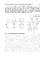
Figure 17 shows the FE-SEM images of three samples (TC1, TC2 and TC3). For all the
samples TiO
2
was grown in form of nanorods whose size was strongly dependent on
conditions of the thermal treatment. These pictures reflect a very high resolution of the FE-
SEM: one can determine approximately both the size on the surface and the depth (or
length) of TiO
2
rods grown in the titanium wafer. Thus, TiO
2
rods in TC2 (annealing time is
1.5 h) were estimated to have a width of about 70 nm on average and a length of about 200
nm. Moreover, a large number of the rods have orientation close to the vertical direction
(see figure 17b). For the TC1 (Figure 17a) and TC3 (Figure 17c) samples, TiO2 rods were
randomly orientated, TCl being thinner than TC3. The annealing time of TC3 was larger
than that of TC2, and TC1, TC2 and TC3 had thicknesses respectively equal to ca. 100, 200
and 150 nm. We also annealed Ti wafers at the temperature of 500°C or 800°C. Even with a
different annealing process, pictures of the nanorods on titanium substrate were similar to
those for TC1 and TC3. This shows that for growing a nanorod-like TiO
2
on titanium
surfaces, the temperature can be maintained at 700°C for 1.5 h.
Figure 18 shows XRD patterns of TC1 (top), TC2 (middle) and TC3 (bottom) samples.
Although the annealed layers of the samples are thin (i.e. ~ 200 nm), in the XRD patterns all
the key characteristic peaks of a rutile TiO
2
crystal are revealed. These peaks correspond to
space distances of 0.322, 0.290, 0.217, 0.205, 0.168, 0.162 and 0.115 nm for all the samples. The
fact that two intensive peaks of the titanium crystal (0.245 and 0.224 nm) occurred proves
that X-ray went through the TiO
2
layer and interacted with the titanium crystalline lattice.
Using formula (2) for the determination of crystalline grain size of the TiO
2
, an average
value calculated for all the TiO
2
peaks was found to be around 100 nm for the TC2 sample.
This value is fairly different for TC1 and TC3 samples. However, these results are in a good
agreement with the results by FE-SEM.
Fig. 17. FE-SEM pictures of annealed titanium surfaces: (a) 700
o
C for 1 h (TC1), (b) 700°C for
1.5 h (TC2) and (c) 700°C for 2 h (TC3). The thickness of nc-TiO
2
layers is of 100 nm, 200 nm
and 150 nm, respectively for TC1, TC2 and TC3 samples
Fig. 18. XRD patterns of nc-TiO
2
layers grown on Ti surfaces at 700
o
C for 1h (TC1), 1.5h
(TC2) and 2h (TC3)
3.2.2 Photoluminescent and electrical properties of hybrid junctions
The results of PL measurements of all the samples excited at a short wavelength (ca. 325nm)
and at a standard one (ca. 470 nm) are presented. Figure 19 shows plots of the PL spectra
measured on MEH-PPV, PON1, PON2 and PON3 samples, using the FL3-2
spectrophotometer with an He-Ne laser as an excitation source ( = 325 nm). It is seen that
all the samples have broad photoemission at two peaks; one higher at 645 nm and another
lower at 605 nm. In a work on MEH-PPV+nc-TiO
2
composite (Carter et al., 1997) the author
reported that two electroluminescence peaks at 580 nm and 640 nm occurred, where the
first peak was higher than the second one. This negligible difference in wavelength values
and intensity of the emission peaks can be explained due to electroluminescence. The
emission peaks are shifted to longer wavelengths with respect to the main absorbance band.
This red-shift is explained due to emission of the most extensively conjugated segments of
the polymer (Kersting et al., 1993). From figure 19, it is seen that photoemission of all the
hybrid samples exhibit higher luminescence intensity than that of the pure MEH-PPV.
However, PL strongest enhancement occurred in PON2 film while for PON1 and PON3
films PL the intensities were not much increased. In these hybrid films no blue shift was
Nanocomposites for Organic Light Emiting Diodes 89
was evaporated on the polymer to make diodes with the structure of AgAl/MEH-
PPV/nc-TiO
2
/Ti (Thuy et. al, 2009).
3.2.1 Morphology and crystalline structure of nanoporous TiO2 layer
Samples which were annealed respectively according to the first, second and third
temperature profile are referred to by TC1, TC2 and TC3. The hybrid films having a
structure of MEH-PPV/Ti-substrate, MEH-PPV/TC1, MEH-PPV/TC2 and MEH-PPV/TC3
are respectively abbreviated to MEHPPV, PON1, PON2 and PON3 for photoluminescence
measurements. Similar symbols are adopted for the heterojunctions samples used in I-V
tests, as follows:
MEHPPV: Ag-Al/MEH-PPV/Ti-substrate/Ag
PON1: Ag-Al/PON1/Ti-substrate/Ag
PON2: Ag-Al/PON2/Ti-substrate/Ag
PON3: Ag-Al/PON3/Ti-substrate/Ag
Figure 17 shows the FE-SEM images of three samples (TC1, TC2 and TC3). For all the
samples TiO
2
was grown in form of nanorods whose size was strongly dependent on
conditions of the thermal treatment. These pictures reflect a very high resolution of the FE-
SEM: one can determine approximately both the size on the surface and the depth (or
length) of TiO
2
rods grown in the titanium wafer. Thus, TiO
2
rods in TC2 (annealing time is
1.5 h) were estimated to have a width of about 70 nm on average and a length of about 200
nm. Moreover, a large number of the rods have orientation close to the vertical direction
(see figure 17b). For the TC1 (Figure 17a) and TC3 (Figure 17c) samples, TiO2 rods were
randomly orientated, TCl being thinner than TC3. The annealing time of TC3 was larger
than that of TC2, and TC1, TC2 and TC3 had thicknesses respectively equal to ca. 100, 200
and 150 nm. We also annealed Ti wafers at the temperature of 500°C or 800°C. Even with a
different annealing process, pictures of the nanorods on titanium substrate were similar to
those for TC1 and TC3. This shows that for growing a nanorod-like TiO
2
on titanium
surfaces, the temperature can be maintained at 700°C for 1.5 h.
Figure 18 shows XRD patterns of TC1 (top), TC2 (middle) and TC3 (bottom) samples.
Although the annealed layers of the samples are thin (i.e. ~ 200 nm), in the XRD patterns all
the key characteristic peaks of a rutile TiO
2
crystal are revealed. These peaks correspond to
space distances of 0.322, 0.290, 0.217, 0.205, 0.168, 0.162 and 0.115 nm for all the samples. The
fact that two intensive peaks of the titanium crystal (0.245 and 0.224 nm) occurred proves
that X-ray went through the TiO
2
layer and interacted with the titanium crystalline lattice.
Using formula (2) for the determination of crystalline grain size of the TiO
2
, an average
value calculated for all the TiO
2
peaks was found to be around 100 nm for the TC2 sample.
This value is fairly different for TC1 and TC3 samples. However, these results are in a good
agreement with the results by FE-SEM.
Fig. 17. FE-SEM pictures of annealed titanium surfaces: (a) 700
o
C for 1 h (TC1), (b) 700°C for
1.5 h (TC2) and (c) 700°C for 2 h (TC3). The thickness of nc-TiO
2
layers is of 100 nm, 200 nm
and 150 nm, respectively for TC1, TC2 and TC3 samples
Fig. 18. XRD patterns of nc-TiO
2
layers grown on Ti surfaces at 700
o
C for 1h (TC1), 1.5h
(TC2) and 2h (TC3)
3.2.2 Photoluminescent and electrical properties of hybrid junctions
The results of PL measurements of all the samples excited at a short wavelength (ca. 325nm)
and at a standard one (ca. 470 nm) are presented. Figure 19 shows plots of the PL spectra
measured on MEH-PPV, PON1, PON2 and PON3 samples, using the FL3-2
spectrophotometer with an He-Ne laser as an excitation source ( = 325 nm). It is seen that
all the samples have broad photoemission at two peaks; one higher at 645 nm and another
lower at 605 nm. In a work on MEH-PPV+nc-TiO
2
composite (Carter et al., 1997) the author
reported that two electroluminescence peaks at 580 nm and 640 nm occurred, where the
first peak was higher than the second one. This negligible difference in wavelength values
and intensity of the emission peaks can be explained due to electroluminescence. The
emission peaks are shifted to longer wavelengths with respect to the main absorbance band.
This red-shift is explained due to emission of the most extensively conjugated segments of
the polymer (Kersting et al., 1993). From figure 19, it is seen that photoemission of all the
hybrid samples exhibit higher luminescence intensity than that of the pure MEH-PPV.
However, PL strongest enhancement occurred in PON2 film while for PON1 and PON3
films PL the intensities were not much increased. In these hybrid films no blue shift was
Organic Light Emitting Diode90
observed, as it was obtained for MEH-PPV + nc- TiO
2
(see figure 13) or for PPV+nc-SiO
2
,
(Yang et al., 2005), as NIP composites. The blue shift was explained by the reduction of the
polymer conjugation chain length. Although PL enhancement has been rarely mentioned,
one can suggest that the increase PL intensity for such a PON2 thin film can be explained by
the large absorption coefficient for TiO
2
nanorods. This similar the effect observed for the
MEHPPV-NIP films, which explained due to the non-radiative Förster resonant energy
transfer (Heliotis et. al., 2006) from TiO
2
nanorods to polymer with excitation of wavelength
less 350 nm.
Fig. 19. PL spectra of MEH-PPV and nanohybrid films by using a He-Ne laser excitation at
325 nm. The best PL enhacement is obtained for PON2 sample
In Figure 20 the PL spectra of MEH-PPV and hybrid film samples with excitation wavelength of
470 nm (on FL3-22 using Xe lamp) are plotted. In this case, the MEH-PPV luminescence
quenching occurred clearest in the PON2 sample. These spectra exhibited quite similarly to the
spectra obtained for the MEH-PPV+nc-TiO
2
(NIP) samples (see figure 14).
Fig. 20. PL spectra of MEH-PPV and nanohybrid films by using a Xe lamp excitation at 470
nm. The strongest MEH-PPV fluorescence quenching is obtained for PON2 sample
For all the samples the photoemission has two broad peaks at 605 nm and 645 nm as in the
case of short wavelength excitation. Moreover, from figure 19 and figure 20 one can see that
in these samples the larger enhancement in PL intensity (under short wavelength
excitation), the stronger fluorescence quenching (under normal excitation) has occurred.
The fact that the peak at 605 nm is larger than the peak at 645 nm is similar to the
electroluminescence spectra plotted in a work of Carter et al (1997). As seen in a work of
Petrella et al (2004), for a NIP composite, in presence of rod-like TiO
2
nanocrystals, PPV
quenching of fluorescence is significantly high. This phenomenon has been explained due to
the transfer of the photogenerated electrons to the TiO
2
. In our case, among three hybrids
films the PON2 sample is the most porous, and the rods are well separated from each other.
Thus this sample is likely to be a NIP composite. Perhaps, this is the reason why PON2
exhibited the strongest quenching effect.
3.2.3 Current-voltage characteristics
Figure 21 shows the I-V curves of a pure MEH-PPV based diode and three hybrid diodes
denoted as PON1, PON2 and PON3. It is seen that such a diode of Ag/Ti/MEHPPV/AlAg
does not have both the transparent anode and hole transport layer (HTL). Thus, stating
from some applied voltage, IV characteristics present a linear dependence of current on
voltage as for a resistance (bottom curve, figure 5). For all the nanohybrid devices a turn-on
voltage is of around 3 V, ascending from PON2 sample to PON1 and PON3, but the current
density is not large (about 5 10 mA/cm
2
at 4 V). For PON2 device although the turn-on
voltage is smaller, the current began increasing with voltage right from 0. For PON1 and
PON3 devices, it grew up from 2 V. This means that in the PON2 the reverse current of the
device appeared from starting switch-on voltage, it can cause the device to be heated up.
The PON1 and PON3 devices have a rather low turn-on voltage and no reverse current was
observed up to an applied voltage of 2 V. It is known (Carter et al., 1997) that the
fluorescence quenching of MEH-PPV results in charge-separation at interfaces of
TiO
2
/MEH-PPV, consequently reducing the barrier height at the last. This indicates that the
PON2 film will be a better candidate for a photovoltaic solar cell than for the OLED.
Fig. 21. I-V characteristics measurement of AgTi/MEH-PPV/Al-Ag (MEHPPV) and three
devices of Ag/Ti/MEH-PPV+nc-TiO
2
/Al-Ag (PON1, PON2 and PON3)
The fact, that PON1 and PON3 samples have very weak fluorescence quenching means that
under the light illumination an inconsiderable electron/hole generation may occur at the
TiO
2
/MEH-PPV interfaces. Therefore, the PON1 and PON3 are not suitable for the
photocurrent conversion. However, the improvement in I-V of the PON1 and PON3 devices
can be attributed to a thin TiO
2
layer sandwiched between the polymer and Ti substrate. In
Nanocomposites for Organic Light Emiting Diodes 91
observed, as it was obtained for MEH-PPV + nc- TiO
2
(see figure 13) or for PPV+nc-SiO
2
,
(Yang et al., 2005), as NIP composites. The blue shift was explained by the reduction of the
polymer conjugation chain length. Although PL enhancement has been rarely mentioned,
one can suggest that the increase PL intensity for such a PON2 thin film can be explained by
the large absorption coefficient for TiO
2
nanorods. This similar the effect observed for the
MEHPPV-NIP films, which explained due to the non-radiative Förster resonant energy
transfer (Heliotis et. al., 2006) from TiO
2
nanorods to polymer with excitation of wavelength
less 350 nm.
Fig. 19. PL spectra of MEH-PPV and nanohybrid films by using a He-Ne laser excitation at
325 nm. The best PL enhacement is obtained for PON2 sample
In Figure 20 the PL spectra of MEH-PPV and hybrid film samples with excitation wavelength of
470 nm (on FL3-22 using Xe lamp) are plotted. In this case, the MEH-PPV luminescence
quenching occurred clearest in the PON2 sample. These spectra exhibited quite similarly to the
spectra obtained for the MEH-PPV+nc-TiO
2
(NIP) samples (see figure 14).
Fig. 20. PL spectra of MEH-PPV and nanohybrid films by using a Xe lamp excitation at 470
nm. The strongest MEH-PPV fluorescence quenching is obtained for PON2 sample
For all the samples the photoemission has two broad peaks at 605 nm and 645 nm as in the
case of short wavelength excitation. Moreover, from figure 19 and figure 20 one can see that
in these samples the larger enhancement in PL intensity (under short wavelength
excitation), the stronger fluorescence quenching (under normal excitation) has occurred.
The fact that the peak at 605 nm is larger than the peak at 645 nm is similar to the
electroluminescence spectra plotted in a work of Carter et al (1997). As seen in a work of
Petrella et al (2004), for a NIP composite, in presence of rod-like TiO
2
nanocrystals, PPV
quenching of fluorescence is significantly high. This phenomenon has been explained due to
the transfer of the photogenerated electrons to the TiO
2
. In our case, among three hybrids
films the PON2 sample is the most porous, and the rods are well separated from each other.
Thus this sample is likely to be a NIP composite. Perhaps, this is the reason why PON2
exhibited the strongest quenching effect.
3.2.3 Current-voltage characteristics
Figure 21 shows the I-V curves of a pure MEH-PPV based diode and three hybrid diodes
denoted as PON1, PON2 and PON3. It is seen that such a diode of Ag/Ti/MEHPPV/AlAg
does not have both the transparent anode and hole transport layer (HTL). Thus, stating
from some applied voltage, IV characteristics present a linear dependence of current on
voltage as for a resistance (bottom curve, figure 5). For all the nanohybrid devices a turn-on
voltage is of around 3 V, ascending from PON2 sample to PON1 and PON3, but the current
density is not large (about 5 10 mA/cm
2
at 4 V). For PON2 device although the turn-on
voltage is smaller, the current began increasing with voltage right from 0. For PON1 and
PON3 devices, it grew up from 2 V. This means that in the PON2 the reverse current of the
device appeared from starting switch-on voltage, it can cause the device to be heated up.
The PON1 and PON3 devices have a rather low turn-on voltage and no reverse current was
observed up to an applied voltage of 2 V. It is known (Carter et al., 1997) that the
fluorescence quenching of MEH-PPV results in charge-separation at interfaces of
TiO
2
/MEH-PPV, consequently reducing the barrier height at the last. This indicates that the
PON2 film will be a better candidate for a photovoltaic solar cell than for the OLED.
Fig. 21. I-V characteristics measurement of AgTi/MEH-PPV/Al-Ag (MEHPPV) and three
devices of Ag/Ti/MEH-PPV+nc-TiO
2
/Al-Ag (PON1, PON2 and PON3)
The fact, that PON1 and PON3 samples have very weak fluorescence quenching means that
under the light illumination an inconsiderable electron/hole generation may occur at the
TiO
2
/MEH-PPV interfaces. Therefore, the PON1 and PON3 are not suitable for the
photocurrent conversion. However, the improvement in I-V of the PON1 and PON3 devices
can be attributed to a thin TiO
2
layer sandwiched between the polymer and Ti substrate. In
Organic Light Emitting Diode92
this case the nc-TiO
2
layer played the role of HTL in OLEDs. Thus, contrarily to the PON2,
such a laminar device as Ag-Al/PON/Ti/Ag is preferable to be used for OLEDs rather than
for polymeric solar cells. However, to make a reverse OLED, instead of AgAl thin film, it is
necessary to deposit a transparent cathode onto the emitting layer.
4. Conclusion and remarks
We have given an overview of the recent works on nanocomposites used for optoelectronic
devices. From the review it is seen that a very rich publication has been issued regarding the
nanostructured composites and nano-hybrid layers or heterojunctions which can be applied
for different practical purposes. Among them there are organic light emitting diodes
(OLED) and excitonic or organic solar cells (OSC).
Our recent achievements on the use of nanocomposites for OLEDs were also presented.
There are two types of the nanocomposite materials, such as nanostructured composites
with a structure of nanoparticles embedded in polymers (abbreviated to NIP) and
nanocomposites with a structure of polymers deposited on nanoporous thin films (called as
PON). Embedding TiO
2
nanoparticles in PEDOT, one can obtain the enhancement of both
the contact of hole transport layer with ITO and the working function of PEDOT films. The
improvement was attributed to the enhancement of the hole current intensity flowing
through the devices. The influence of nanooxides on the photoelectric properties of the NIPs
is explained with regard to the fact that TiO
2
particles usually form a type-II heterojunction
with a polymer matrix, which essentially results in the separation of nonequilibrium
electrons and holes. NIPs with the TiO
2
nanoparticles in MEH-PPV have been studied as
photoactive material. MEH-PPV luminescence quenching is strongly dependent on the
nature of nanostructral particles embedded in polymer matrix. Actually, the higher
quenching of the polymer fluorescence observed in presence of titania nanoparticles proves
that transfer of the photogenerated electrons to TiO
2
is more efficient for rods.
Characterization of the nanocomposite films showed that both the current-voltage (I-V)
characteristics and the photoluminescent properties of the NIP nanocomposite materials
were significantly enhanced in comparison with the standard polymers. OLEDs made from
these layers can exhibit a large photonic efficiency. For a PON-like hybrid layer of MEH-
PPV/nc-TiO
2
, the photoluminescence enhancement has also been observed. Thin
nanostructured TiO
2
layers were grown by thermal annealing, then they were spin-coated
by MEH-PPV films. Study of PL spectra of pure MEH-PPV and MEHPPV-PON films has
shown that with excitation by a 331.1 nm wavelength laser lead to the largest enhancement
in photoluminescent intensity as observed in the PON samples, and with an excitation of a
470 nm wavelength laser, the strongest fluorescence quenching occurred in this sample too.
Current-voltage characteristics of laminar layer devices with a structure of Ti/PON/Al-Ag
in comparison with that of Ti/MEH-PPV/Al-Ag showed that the turn-on voltage of the
devices was lowered considerably. Combining I-V with SEM and PL, it is seen that PON are
suitable for an reverse OLED, where the light goes out through the transparent or semi-
transparent cathode, moreover to do Ohmic contact to the metallic Ti electrode is much
easier.
However, to realize making reverse OLEDs, it is necessary to carry-out both the theoretical
and technological researches to find out appropriate materials which can be used for the
transparent cathode.
Acknowledgement
This work was supported by the Vietnam National Foundation for Science and Technology
Development (NAFOSTED) in the period 2010 – 2011 (Project Code: 103.02.88.09).
5. References
Burlakov, V. M.; Kawata, K.; Assender, H. E.; Briggs, G. A. D.; Ruseckas, A. & Samuel, I. D.
W. (2005). Discrete hopping model of exciton transport in disordered media.
Physical Review 72, pp. 075206-1 ÷ 075206-5.
Carter, S. A.; Scott, J. C. & Brock, J. (1997). Enhanced luminance in polymer composite light
emitting diodes. J. Appl. Phys. 71(9), pp. 1145 – 1147.
Cullity, B. D. (1978). Elements of X-Ray diffraction, 2nd ed., p.102. Addison, Wesley Publishing
Company, Inc., Reading, MA.
Dinh, N. N.; Chi L. H., Thuy, T.T.C; Trung T.Q. & Vo, Van Truong. (2009). Enhancement of
current, voltage characteristics of multilayer organic light emitting diodes by using
nanostructured composite films, J. Appl. Phys. 105, pp. 093518-1÷ 093518-7.
Dinh, N. N.; Chi, L. H.; Thuy, T. T. C.; Thanh, D. V. & Nguyen, T. P. (2008). Study of
nanostructured polymeric composites and hybrid layers used for Light Emitting
Diodes. J. Korean Phys. Soc. 53, pp. 802-805.
Dinh, N. N.; Trung, T. Q.; Le H. M.; Long P. D. & Nguyen T., P. (2003). Multiplayer Organic
Light Emmiting Diodes: Thin films preparation and Device characterization,
Communications in Physics 13, pp. 165-170.
Dittmer, J. J.; Marseglia, E. A. & Friend, R. H. (2000). Electron Trapping in Dye/Polymer
Blend Photovoltaic Cells. Adv. Mater. 12, pp.1270-1274.
Haugeneder, A.; Neges, M.; Kallinger, C.; Spirkl, W.; Lemmer, U. & Felmann, J. (1999).
Exciton diffusion and dissociation in conjugated polymer/fullerene blends and
heterostructures. Phys. Rev. B, 59, pp. 15346–15351.
Heliotis, G.; Itskos, G.; Murray, R.; Dawson, M. D.; Watson, I. M. & Bradley, D. D. C. (2006).
Hybrid inorganic/organic semiconductor heterostructures with efficient non,
radiative Förster energy transfer. Adv. Mater. 18, pp. 334-341.
Huynh, W. U.; Dittmer, J. J. & Alivisatos, A. P. (2002). Hybrid Nanorod, Polymer Solar Cells.
Science 295, pp. 2425 – 2427.
Kersting, R.; Lemmer, U.; Marht, R. F.; Leo, K.; Kurz, H.; Bassler, H. & Gobel, E. O. (1993).
Femtosecond energy relaxation in π, conjugated polymers. Phys. Rev. Lett. 70, pp.
3820 – 3823.
Klabunde, K. J. (2001). Nanoscale Materials in Chemistry, John Wiley & Sons.
Lin, Yu, Ting.; Zeng, Tsung, Wei.; Lai, Wei, Zong.; Chen, Chun, Wei.; Lin, Yun, Yue.; Chang,
Yu, Sheng. & Su, Wei, Fang. (2006). Efficient photoinduced charge transfer in TiO
2
nanorod/conjugated polymer hybrid materials. Nanotechnology 17, pp. 5781–5785.
Ma, W.; Yang, C.; Gong, X.; Lee, K. & Heeger, A. J. (2005). Thermally Stable, Efficient
Polymer Solar Cells with Nanoscale Control of the Interpenetrating Network
Morphology. Adv. Func. Mater. 15, pp.1617 – 1622.
Petrella, T. M.; Cozzoli, P. D.; Curri, M. L.; Striccoli, M.; Cosma, P.; Farinola, G. M.; Babudri,
F.; Naso, F. & Agostiano, A. (2004). TiO
2
nanocrystals – MEH, PPV composite thin
films as photoactive material. Thin Solid Films 451/452, pp. 64–68.
Nanocomposites for Organic Light Emiting Diodes 93
this case the nc-TiO
2
layer played the role of HTL in OLEDs. Thus, contrarily to the PON2,
such a laminar device as Ag-Al/PON/Ti/Ag is preferable to be used for OLEDs rather than
for polymeric solar cells. However, to make a reverse OLED, instead of AgAl thin film, it is
necessary to deposit a transparent cathode onto the emitting layer.
4. Conclusion and remarks
We have given an overview of the recent works on nanocomposites used for optoelectronic
devices. From the review it is seen that a very rich publication has been issued regarding the
nanostructured composites and nano-hybrid layers or heterojunctions which can be applied
for different practical purposes. Among them there are organic light emitting diodes
(OLED) and excitonic or organic solar cells (OSC).
Our recent achievements on the use of nanocomposites for OLEDs were also presented.
There are two types of the nanocomposite materials, such as nanostructured composites
with a structure of nanoparticles embedded in polymers (abbreviated to NIP) and
nanocomposites with a structure of polymers deposited on nanoporous thin films (called as
PON). Embedding TiO
2
nanoparticles in PEDOT, one can obtain the enhancement of both
the contact of hole transport layer with ITO and the working function of PEDOT films. The
improvement was attributed to the enhancement of the hole current intensity flowing
through the devices. The influence of nanooxides on the photoelectric properties of the NIPs
is explained with regard to the fact that TiO
2
particles usually form a type-II heterojunction
with a polymer matrix, which essentially results in the separation of nonequilibrium
electrons and holes. NIPs with the TiO
2
nanoparticles in MEH-PPV have been studied as
photoactive material. MEH-PPV luminescence quenching is strongly dependent on the
nature of nanostructral particles embedded in polymer matrix. Actually, the higher
quenching of the polymer fluorescence observed in presence of titania nanoparticles proves
that transfer of the photogenerated electrons to TiO
2
is more efficient for rods.
Characterization of the nanocomposite films showed that both the current-voltage (I-V)
characteristics and the photoluminescent properties of the NIP nanocomposite materials
were significantly enhanced in comparison with the standard polymers. OLEDs made from
these layers can exhibit a large photonic efficiency. For a PON-like hybrid layer of MEH-
PPV/nc-TiO
2
, the photoluminescence enhancement has also been observed. Thin
nanostructured TiO
2
layers were grown by thermal annealing, then they were spin-coated
by MEH-PPV films. Study of PL spectra of pure MEH-PPV and MEHPPV-PON films has
shown that with excitation by a 331.1 nm wavelength laser lead to the largest enhancement
in photoluminescent intensity as observed in the PON samples, and with an excitation of a
470 nm wavelength laser, the strongest fluorescence quenching occurred in this sample too.
Current-voltage characteristics of laminar layer devices with a structure of Ti/PON/Al-Ag
in comparison with that of Ti/MEH-PPV/Al-Ag showed that the turn-on voltage of the
devices was lowered considerably. Combining I-V with SEM and PL, it is seen that PON are
suitable for an reverse OLED, where the light goes out through the transparent or semi-
transparent cathode, moreover to do Ohmic contact to the metallic Ti electrode is much
easier.
However, to realize making reverse OLEDs, it is necessary to carry-out both the theoretical
and technological researches to find out appropriate materials which can be used for the
transparent cathode.
Acknowledgement
This work was supported by the Vietnam National Foundation for Science and Technology
Development (NAFOSTED) in the period 2010 – 2011 (Project Code: 103.02.88.09).
5. References
Burlakov, V. M.; Kawata, K.; Assender, H. E.; Briggs, G. A. D.; Ruseckas, A. & Samuel, I. D.
W. (2005). Discrete hopping model of exciton transport in disordered media.
Physical Review 72, pp. 075206-1 ÷ 075206-5.
Carter, S. A.; Scott, J. C. & Brock, J. (1997). Enhanced luminance in polymer composite light
emitting diodes. J. Appl. Phys. 71(9), pp. 1145 – 1147.
Cullity, B. D. (1978). Elements of X-Ray diffraction, 2nd ed., p.102. Addison, Wesley Publishing
Company, Inc., Reading, MA.
Dinh, N. N.; Chi L. H., Thuy, T.T.C; Trung T.Q. & Vo, Van Truong. (2009). Enhancement of
current, voltage characteristics of multilayer organic light emitting diodes by using
nanostructured composite films, J. Appl. Phys. 105, pp. 093518-1÷ 093518-7.
Dinh, N. N.; Chi, L. H.; Thuy, T. T. C.; Thanh, D. V. & Nguyen, T. P. (2008). Study of
nanostructured polymeric composites and hybrid layers used for Light Emitting
Diodes. J. Korean Phys. Soc. 53, pp. 802-805.
Dinh, N. N.; Trung, T. Q.; Le H. M.; Long P. D. & Nguyen T., P. (2003). Multiplayer Organic
Light Emmiting Diodes: Thin films preparation and Device characterization,
Communications in Physics 13, pp. 165-170.
Dittmer, J. J.; Marseglia, E. A. & Friend, R. H. (2000). Electron Trapping in Dye/Polymer
Blend Photovoltaic Cells. Adv. Mater. 12, pp.1270-1274.
Haugeneder, A.; Neges, M.; Kallinger, C.; Spirkl, W.; Lemmer, U. & Felmann, J. (1999).
Exciton diffusion and dissociation in conjugated polymer/fullerene blends and
heterostructures. Phys. Rev. B, 59, pp. 15346–15351.
Heliotis, G.; Itskos, G.; Murray, R.; Dawson, M. D.; Watson, I. M. & Bradley, D. D. C. (2006).
Hybrid inorganic/organic semiconductor heterostructures with efficient non,
radiative Förster energy transfer. Adv. Mater. 18, pp. 334-341.
Huynh, W. U.; Dittmer, J. J. & Alivisatos, A. P. (2002). Hybrid Nanorod, Polymer Solar Cells.
Science 295, pp. 2425 – 2427.
Kersting, R.; Lemmer, U.; Marht, R. F.; Leo, K.; Kurz, H.; Bassler, H. & Gobel, E. O. (1993).
Femtosecond energy relaxation in π, conjugated polymers. Phys. Rev. Lett. 70, pp.
3820 – 3823.
Klabunde, K. J. (2001). Nanoscale Materials in Chemistry, John Wiley & Sons.
Lin, Yu, Ting.; Zeng, Tsung, Wei.; Lai, Wei, Zong.; Chen, Chun, Wei.; Lin, Yun, Yue.; Chang,
Yu, Sheng. & Su, Wei, Fang. (2006). Efficient photoinduced charge transfer in TiO
2
nanorod/conjugated polymer hybrid materials. Nanotechnology 17, pp. 5781–5785.
Ma, W.; Yang, C.; Gong, X.; Lee, K. & Heeger, A. J. (2005). Thermally Stable, Efficient
Polymer Solar Cells with Nanoscale Control of the Interpenetrating Network
Morphology. Adv. Func. Mater. 15, pp.1617 – 1622.
Petrella, T. M.; Cozzoli, P. D.; Curri, M. L.; Striccoli, M.; Cosma, P.; Farinola, G. M.; Babudri,
F.; Naso, F. & Agostiano, A. (2004). TiO
2
nanocrystals – MEH, PPV composite thin
films as photoactive material. Thin Solid Films 451/452, pp. 64–68.
Organic Light Emitting Diode94
Quyang, J.; Chu, C., W.; Chen, F., C.; Xu, Q. & Yang, Y. (2005). High, Conductivity Poly(3,4,
ethylenedioxythiophene): Poly(styrene sulfonate) Film and Its Application in
Polymer Optoelectronic Devices. Advanced Functional Materials 15, pp. 203 - 208.
Quyang, J.; Xu, Q.; Chu, C., W.; Yang, Y.; Li, G. & Shinar, J. (2004). On the mechanism of
conductivity enhancement in poly(3,4, ethylenedioxythiophene):poly(styrene
sufonate) film through solvent treatment. Polymer 45, pp. 8443 - 8450.
Ravirajan, P.; Bradley, D. D. C.; Nelson, J.; Haque, S. A.; Durrant, J. R.; Smit, H. J. P. &
Kroon, J. M. (2005). Efficient charge collection in hybrid polymer/TiO
2
solar cells
using poly(ethylenedioxythiophene)/polystyrene sulphonate as hole collector.
Appl. Phys. Lett. 86, pp. 143101 - 143113.
Salafsky, J. S. (1999). Exciton dissociation, charge transport, and recombination in ultrathin,
conjugated polymer, TiO2 nanocrystal intermixed composites. Physical Review B 59,
pp. 10885 – 10894.
Scott, J. C.; Kaufman, J.; Brock, P. J.; DiPietro, R.; Salem, J. & Goitia, J. A. (1996). MEH, PPV
Light, Emitting Diodes: Mechanisms of Failure. J. Appl. Phys. 79, pp. 2745 – 2753.
Tehrani, P.; Kanciurzewska, A.; Crispin, X.; Robinson, N. D.; Fahlman, M. & Berggren, M.
(2007). The effect of pH on the electrochemical over, oxidation in PEDOT:PSS films.
Solid State Ionics 177, pp. 3521 – 3528.
Thuy, T. T.C.; Chi, L. H. & Dinh, N. N. (2009). Study of Photoluminescent and Electrical
Properties of Nanostructured MEH, PPV/ TiO
2
hybrid films, JKPS 54, pp. 291 - 295.
Yang, S. H.; Nguyen, T. P.; Le Rendu, P. & Hsu, C. S. (2005). Optical and electrical properties
of PPV/SiO
2
and PPV/TiO
2
composite materials. Composites Part A: Appl.
Sci Manufact. 36, pp. 509 - 513.
Carrier Transport and Recombination Dynamics in Disordered Organic Light Emitting Diodes 95
Carrier Transport and Recombination Dynamics in Disordered Organic
Light Emitting Diodes
Shih-Wei Feng and Hsiang-Chen Wang
X
Carrier Transport and Recombination
Dynamics in Disordered Organic
Light Emitting Diodes
Shih-Wei Feng
1
and Hsiang-Chen Wang
2
1
Department of Applied Physics, National University of Kaohsiung, Taiwan, R.O.C.
2
Graduate Institute of Opto-Mechatronics, National Chung Cheng University, Chia-Yi,
Taiwan, R.O.C.
1. Introduction
Organic light emitting diode (OLED) displays are forecast to be the promising display
technology. They are thin, flexible, energy conserving, and suitable for large screen displays.
For the developments of high-performance devices, high efficiency and good color purity
are necessary. The emission wavelengths can be modified by blending dopants into the
polymers light emitting diodes or by the incorporation of fluorescent dyes into the emissive
layers for small molecule devices. The incorporation of fluorescent dyes into host materials
has the advantages of efficient color tuning, good device efficiency, and narrow emission
spectrum width [1-4].
In OLEDs, carriers are localized in molecules and charge transport is a hopping process [2].
Carrier mobility is determined by charge transport between neighboring hopping sites. The
mobility usually shows the Poole-Frenkel characteristic [5]. By controlling the distance
between hopping sites, carrier mobility can be adjusted [6]. At thermodynamic equilibrium,
charge carriers mostly occupy the deep tail states of the density-of-states (DOS) distribution
[7]. Carrier hopping occurs mostly via shallower states [8,9]. This shows that carrier density
could affect mobility. Furthermore, dopants in OLEDs act as shallow trapping centers,
which trap carriers and change the carrier density. Carrier trapping is the main emission
mechanism in doped organic systems [10]. This also shows the dependence of the mobility
on the dopant concentration. Although the efficiency of doped OLEDs has been improved,
the carrier dynamics have not been well discussed [1-4]. To further improve the efficiency
and lifetimes of OLEDs, the carrier transport as well as recombination dynamics of doped
OLEDs should be well explored.
In this study, the dependences of carrier transport behavior and luminescence mechanism
on dopant concentration of OLEDs were studied. In the lightly-doped sample, higher carrier
mobility and better device performance were observed. This shows that dopants create
additional hopping sites and shorten the hopping distance. At a higher dopant
concentration, dopants tend to aggregate and the aggregations degrade the device
performance. In addition, the observed decay rates and luminescence efficiencies of the
5
Organic Light Emitting Diode96
doped samples can be used to calculate the radiative and nonradiative decay rates. The
trend suggests that the lightly-doped sample can exhibit better luminescence efficiency at
higher applied voltage while the highly-doped sample shows poorer luminescence
efficiency even operated at lower applied voltage. The resulting recombination dynamics
can be used to explain the device characteristics and performance of the doped samples.
2. Sample Structures and Experimental Procedures
The OLEDs are fabricated by vacuum deposition of the organic materials onto an indium-
tin-oxide (ITO)-coated glass at a deposition rate of l-2Å s
-l
at l0
-6
Torr. The device structures
are ITO/N, N'-bis(naphthalen-1-yl)-N, N'-bis(phenyl) benzidine (NPB: 55nm) /Tris(8-
quinolinolato)-aluminum(A1q
3
) : 10-(2-benzothiazolyl)-1, 1, 7, 7-tetramethyl-2, 3, 6, 7-
tetrahydro-lH, 5H, 11H-benzo[l]pyrano[6, 7, 8-і ј] quinolizin-11-one (C545T:40nm)/Alq
3
(40nm)/LiF(1nm)/Al(200nm). NPB and Alq
3
are used as the hole transport layer (HTL) and
electron transporting layer (ETL), respectively. The dopant concentrations of C545T in A1q
3
are 1%, 3%, and 7%. The active areas of each device were 9 mm
2
. A blank sample (no
doping) was also prepared for comparison. Figure 1 shows the sample structures of OLEDs.
Fig. 1. Sample structures of OLEDs.
The morphological study was done by a scanning electron microscopy (SEM) (Hitachi
Model S-4300N) with the excitation 5kV electrons. The electroluminescence (EL) spectra
were measured by a Hitachi (model 4500) fluorescence spectrometer together with a power
supply. Current-voltage (I-V) and capacitance-voltage (C-V) characteristics were measured
with a semiconductor parameter analyzer (Agilent 4145B) and a LCR meter (Agilent 4284),
respectively.
For transient electroluminescence measurements, a pulse generator (Agilent 8114A 100 V/2)
was used to generate rectangular voltage pulses to the devices. The repetition rate and
width of the pulse were l kHz and 5 µs, respectively. The light output was detected by a
fast-biased silicon photodiode (Electro-Optics Technology Inc., model:ET-2020) operating
directly on the surface of the devices. The transit time is a function of both the time required
to charge the device (a function of the RC time constant of the circuit) and mobility [11]. In
order to reduce the contribution of the time to charge the device, attention was paid to the
RC time constant of the EL cells. The maximum measured capacitance, C, of the EL cells was
about 6 nF. The series resistance of our cells was estimated to be about 10 Ω. Therefore, the
RC time constant was estimated to be less than 60 ns and the selected pulse width was
greater than the charging time of the devices [4,12]. The temporal evolutions of EL signals
were recorded by the average mode of a 50Ω input resistance of a digital oscilloscope
(Agilent Model DSO 6052A, 500 MHz/4Gs/s). The oscilloscope was triggered by the pulse
generator. The two coaxial cables for measuring transit EL and voltage pulse were equal in
length, so that the time delay, except for the intrinsic delay, was negligible. All the
measurements were carried out at room temperature (RT).
3. Experimental Results
3.1 SEM Images and EL Spectra (9 pt, bold)
Figure 2 (a) and (b) shows the SEM images of 1% and 3% C545T-doped Alq
3
films,
respectively. The morphology of 1% C545T-doped Alq
3
film shows a homogeneous and flat
image while that of 3% C545T-doped Alq
3
shows aggregations. This shows that dopants
tend to aggregate as the dopant concentration becomes higher.
(a) (b)
Fig. 2. SEM images of (a) 1% and (b) 3% C545T-doped Alq
3
films.
Figure 3 shows the EL spectra of 1%, 3%, and 7% C545T-doped Alq
3
samples and the
undoped one. The EL spectra of the doped samples are significantly narrower than that of
the undoped one. This is a tremendous advantage in the color mixing of red, green, and blue
light for full-color applications. In order to create saturated colors, it is important for the
individual red, green, and blue to be as pure as possible. Furthermore, as the dopant
concentration increases, the peak position was slightly red-shifted and a shoulder in the
long-wavelength side becomes apparent. Similar phenomena were also observed in Alq
3
films with 4-(dicyanomethylene)-2-methyl-6-(p-dimethylaminostyryl)-4H-pyran doapnt
(DCM) aggregations [1,13,14]. The aggregations not only represent spatially distributed
potential minimums but also broaden the effective DOS distribution. Hence, the broader
spectrum width and the long-wavelength shoulder in EL spectra imply a larger degree of
disorder.
Carrier Transport and Recombination Dynamics in Disordered Organic Light Emitting Diodes 97
doped samples can be used to calculate the radiative and nonradiative decay rates. The
trend suggests that the lightly-doped sample can exhibit better luminescence efficiency at
higher applied voltage while the highly-doped sample shows poorer luminescence
efficiency even operated at lower applied voltage. The resulting recombination dynamics
can be used to explain the device characteristics and performance of the doped samples.
2. Sample Structures and Experimental Procedures
The OLEDs are fabricated by vacuum deposition of the organic materials onto an indium-
tin-oxide (ITO)-coated glass at a deposition rate of l-2Å s
-l
at l0
-6
Torr. The device structures
are ITO/N, N'-bis(naphthalen-1-yl)-N, N'-bis(phenyl) benzidine (NPB: 55nm) /Tris(8-
quinolinolato)-aluminum(A1q
3
) : 10-(2-benzothiazolyl)-1, 1, 7, 7-tetramethyl-2, 3, 6, 7-
tetrahydro-lH, 5H, 11H-benzo[l]pyrano[6, 7, 8-і ј] quinolizin-11-one (C545T:40nm)/Alq
3
(40nm)/LiF(1nm)/Al(200nm). NPB and Alq
3
are used as the hole transport layer (HTL) and
electron transporting layer (ETL), respectively. The dopant concentrations of C545T in A1q
3
are 1%, 3%, and 7%. The active areas of each device were 9 mm
2
. A blank sample (no
doping) was also prepared for comparison. Figure 1 shows the sample structures of OLEDs.
Fig. 1. Sample structures of OLEDs.
The morphological study was done by a scanning electron microscopy (SEM) (Hitachi
Model S-4300N) with the excitation 5kV electrons. The electroluminescence (EL) spectra
were measured by a Hitachi (model 4500) fluorescence spectrometer together with a power
supply. Current-voltage (I-V) and capacitance-voltage (C-V) characteristics were measured
with a semiconductor parameter analyzer (Agilent 4145B) and a LCR meter (Agilent 4284),
respectively.
For transient electroluminescence measurements, a pulse generator (Agilent 8114A 100 V/2)
was used to generate rectangular voltage pulses to the devices. The repetition rate and
width of the pulse were l kHz and 5 µs, respectively. The light output was detected by a
fast-biased silicon photodiode (Electro-Optics Technology Inc., model:ET-2020) operating
directly on the surface of the devices. The transit time is a function of both the time required
to charge the device (a function of the RC time constant of the circuit) and mobility [11]. In
order to reduce the contribution of the time to charge the device, attention was paid to the
RC time constant of the EL cells. The maximum measured capacitance, C, of the EL cells was
about 6 nF. The series resistance of our cells was estimated to be about 10 Ω. Therefore, the
RC time constant was estimated to be less than 60 ns and the selected pulse width was
greater than the charging time of the devices [4,12]. The temporal evolutions of EL signals
were recorded by the average mode of a 50Ω input resistance of a digital oscilloscope
(Agilent Model DSO 6052A, 500 MHz/4Gs/s). The oscilloscope was triggered by the pulse
generator. The two coaxial cables for measuring transit EL and voltage pulse were equal in
length, so that the time delay, except for the intrinsic delay, was negligible. All the
measurements were carried out at room temperature (RT).
3. Experimental Results
3.1 SEM Images and EL Spectra (9 pt, bold)
Figure 2 (a) and (b) shows the SEM images of 1% and 3% C545T-doped Alq
3
films,
respectively. The morphology of 1% C545T-doped Alq
3
film shows a homogeneous and flat
image while that of 3% C545T-doped Alq
3
shows aggregations. This shows that dopants
tend to aggregate as the dopant concentration becomes higher.
(a) (b)
Fig. 2. SEM images of (a) 1% and (b) 3% C545T-doped Alq
3
films.
Figure 3 shows the EL spectra of 1%, 3%, and 7% C545T-doped Alq
3
samples and the
undoped one. The EL spectra of the doped samples are significantly narrower than that of
the undoped one. This is a tremendous advantage in the color mixing of red, green, and blue
light for full-color applications. In order to create saturated colors, it is important for the
individual red, green, and blue to be as pure as possible. Furthermore, as the dopant
concentration increases, the peak position was slightly red-shifted and a shoulder in the
long-wavelength side becomes apparent. Similar phenomena were also observed in Alq
3
films with 4-(dicyanomethylene)-2-methyl-6-(p-dimethylaminostyryl)-4H-pyran doapnt
(DCM) aggregations [1,13,14]. The aggregations not only represent spatially distributed
potential minimums but also broaden the effective DOS distribution. Hence, the broader
spectrum width and the long-wavelength shoulder in EL spectra imply a larger degree of
disorder.
Organic Light Emitting Diode98
-1 0 1 2 3 4
0
2
4
6
Capacitance (nF)
Voltage (volt)
alq3 +7% C545T
alq3+3% C545T
alq3+1% C545T
0 2 4 6 8 10 12
0
10
20
30
40
50
60
Current density (A/cm
2
)
Applied Voltage (volt)
alq3
alq3 +1% C545T
alq3 +3% C545T
alq3 +7% C545T
Fig. 3. EL spectra of the undoped and 1%, 3%, and 7% C545T-doped Alq
3
samples at RT.
3.2 I-V and C-V Characteristics
Figure 4(a) shows the current density versus applied voltage (I-V) characteristic of the four
samples. Compared with the doped samples, the undoped sample shows a higher
operational threshold and a shallow slope of current density versus applied voltage. This
shows that the incorporation of dopants into host materials can improve device
performance. In addition, with a higher dopant concentration, the driving voltage is higher
and the current density is lower. This suggests that the aggregations tend to degrade the
device performance.
(a) (b)
Fig. 4. (a) Current density versus applied voltage (I-V) characteristics of the undoped and
three doped samples;(b) the differential capacitance as a function of bias (C-V) at a fixed
frequency of 10 Hz of the three doped samples.
0 1 2 3 4 5 6 7
0.00
0.05
0.10
0.15
Intensity (arb.unit)
Time (s)
13 V
11 V
9 V
7 V
5 V
3 V
0 5 10 15
0.0
0.5
1.0
1.5
2.0
2.5
3.0
Voltage (volt)
alq3+1% C545T
alq3+3% C545T
alq3+7% C545T
Response Time (s)
Furthermore, Figure 4(b) shows the differential capacitance
dVdQC /
as a function of bias
for a fixed frequency 10 Hz. No apparent difference was observed for negative bias. For the
positive bias, the capacitance increases significantly and reaches a maximum at the
“transition voltage V
0
”. V
0
is regarded as the built-in voltage V
bi
, ie. the difference in work
function between the two contacts [15]. The transition voltages V
0
for 1%, 3% and 7% C545T-
doped Alq
3
samples are 2.3, 2.38 and 2.6 volts, respectively. Aggregations can trap carriers
for self-quenching and luminescence losses, which leads to a higher turn-on voltage in the
highly-doped sample. This argument is consistent with the long-wavelength shoulder in the
EL spectrum. Furthermore, as the applied voltage is beyond V
0
, the electrons and holes start
to recombine and the capacitance decreases. The negative slope is related to the
recombination efficiency. The lower the capacitance, the better the recombination efficiency.
The slower decreasing trend of the highly-doped samples
implies a low recombination
efficiency.
3.3 Carrier Transport and Recombination Dynamics
The dynamic behavior of EL under electrical fast-pulse excitation provides important
insights into the carrier transport behaviors and internal operation mechanisms of OLEDs.
The response time is determined by the time delay, t
d
, between addressing the device with a
short, rectangular voltage pulse and the first appearance of EL [16,17]. The EL onset is
identified as the time at which the two leading fronts of injected holes and electrons meet in
the device. The time after the EL tends to saturate is the time at which electron and hole
distributions have interpenetrated. The temporal decay of the EL at the end of the applied
voltage pulse reflects the depletion of the carrier reservoir established during the preceding
on-phase. Because the doped samples performed better than the blank one, the discussions
in this section were focused on the three doped samples.
Figure 5(a) shows the transient EL as a function of time for different applied voltages for 1%
C545T-doped Alq
3
sample. With increasing applied voltage, a shorter time delay (i.e. an
earlier EL onset) and a steeper rise of the transient EL were observed. This shows a faster
response time and more carrier mobility.
(a) (b)
Fig. 5. (a) The transient EL as a function of time for different applied voltages for 1% C545T-
doped Alq
3
sample. (b) Response time as a function of applied voltage for three doped
samples.
Carrier Transport and Recombination Dynamics in Disordered Organic Light Emitting Diodes 99
-1 0 1 2 3 4
0
2
4
6
Capacitance (nF)
Voltage (volt)
alq3 +7% C545T
alq3+3% C545T
alq3+1% C545T
0 2 4 6 8 10 12
0
10
20
30
40
50
60
Current density (A/cm
2
)
Applied Voltage (volt)
alq3
alq3 +1% C545T
alq3 +3% C545T
alq3 +7% C545T
Fig. 3. EL spectra of the undoped and 1%, 3%, and 7% C545T-doped Alq
3
samples at RT.
3.2 I-V and C-V Characteristics
Figure 4(a) shows the current density versus applied voltage (I-V) characteristic of the four
samples. Compared with the doped samples, the undoped sample shows a higher
operational threshold and a shallow slope of current density versus applied voltage. This
shows that the incorporation of dopants into host materials can improve device
performance. In addition, with a higher dopant concentration, the driving voltage is higher
and the current density is lower. This suggests that the aggregations tend to degrade the
device performance.
(a) (b)
Fig. 4. (a) Current density versus applied voltage (I-V) characteristics of the undoped and
three doped samples;(b) the differential capacitance as a function of bias (C-V) at a fixed
frequency of 10 Hz of the three doped samples.
0 1 2 3 4 5 6 7
0.00
0.05
0.10
0.15
Intensity (arb.unit)
Time (s)
13 V
11 V
9 V
7 V
5 V
3 V
0 5 10 15
0.0
0.5
1.0
1.5
2.0
2.5
3.0
Voltage (volt)
alq3+1% C545T
alq3+3% C545T
alq3+7% C545T
Response Time (s)
Furthermore, Figure 4(b) shows the differential capacitance
dVdQC /
as a function of bias
for a fixed frequency 10 Hz. No apparent difference was observed for negative bias. For the
positive bias, the capacitance increases significantly and reaches a maximum at the
“transition voltage V
0
”. V
0
is regarded as the built-in voltage V
bi
, ie. the difference in work
function between the two contacts [15]. The transition voltages V
0
for 1%, 3% and 7% C545T-
doped Alq
3
samples are 2.3, 2.38 and 2.6 volts, respectively. Aggregations can trap carriers
for self-quenching and luminescence losses, which leads to a higher turn-on voltage in the
highly-doped sample. This argument is consistent with the long-wavelength shoulder in the
EL spectrum. Furthermore, as the applied voltage is beyond V
0
, the electrons and holes start
to recombine and the capacitance decreases. The negative slope is related to the
recombination efficiency. The lower the capacitance, the better the recombination efficiency.
The slower decreasing trend of the highly-doped samples
implies a low recombination
efficiency.
3.3 Carrier Transport and Recombination Dynamics
The dynamic behavior of EL under electrical fast-pulse excitation provides important
insights into the carrier transport behaviors and internal operation mechanisms of OLEDs.
The response time is determined by the time delay, t
d
, between addressing the device with a
short, rectangular voltage pulse and the first appearance of EL [16,17]. The EL onset is
identified as the time at which the two leading fronts of injected holes and electrons meet in
the device. The time after the EL tends to saturate is the time at which electron and hole
distributions have interpenetrated. The temporal decay of the EL at the end of the applied
voltage pulse reflects the depletion of the carrier reservoir established during the preceding
on-phase. Because the doped samples performed better than the blank one, the discussions
in this section were focused on the three doped samples.
Figure 5(a) shows the transient EL as a function of time for different applied voltages for 1%
C545T-doped Alq
3
sample. With increasing applied voltage, a shorter time delay (i.e. an
earlier EL onset) and a steeper rise of the transient EL were observed. This shows a faster
response time and more carrier mobility.
(a) (b)
Fig. 5. (a) The transient EL as a function of time for different applied voltages for 1% C545T-
doped Alq
3
sample. (b) Response time as a function of applied voltage for three doped
samples.
Organic Light Emitting Diode100
0.0 0.1 0.2 0.3 0.4 0.5 0.6 0.7
0.00
0.05
0.10
0.15
Intensity (arb.unit)
Time (ms)
13 Volt
11 Volt
9 Volt
7 Volt
5 Volt
3 Volt
The response time as a function of the applied voltage for the three samples are shown in
Figure 5(b). At low applied voltages ( volts8
applied
V ), the response time increases with
dopant concentration. In the highly-doped sample, some carriers are trapped and then
quenched in aggregations. This slows down carrier mobility and decreases the overlap
integral of electron-hole wavefunctions. Hence, the response time is longer. On the other
hand, with high applied voltages ( volts8
applied
V ), carriers have more mobility among the
hopping sites so that carriers may not be quenched in aggregations. This leads to the
response times nearly independent of dopant concentration. The constant response time
within the large bias range ( volts11
applied
V ) implies a saturation of carrier mobility.
The transient EL decay as a function of time for different applied voltages for 1% C545T-
doped Alq
3
sample is shown in Figure 6. The EL decay can be fitted with a single
exponential to obtain decay time. Figure 7(a) shows the decay time as a function of applied
voltage for the three doped samples. The decay rate
)/1(
, the reciprocal of the decay
time (τ), is shown in Figure 7(b). The decay rate shows an increasing and then decreasing
trend with increasing applied voltage. It is noted that the measured decay rate is the sum of
the radiative decay rate and nonradiative decay rate by the following equation [18]:
1
r nr
(1)
where κ
r
, κ
nr
, and κ are the radiative decay rate, nonradiative decay rate, and total decay
rate, respectively. At somewhat high applied voltages ( volts5
applied
V ), the slower decay
rate may imply an enhanced nonradiative decay rate. The details will be discussed later.
Fig. 6. The transient EL decay as a function of time for different applied voltages for 1%
C545T-doped Alq
3
sample at RT.
Fig. 7. (a) Decay times as well as (b) decay rates as a function of applied voltage for the three
doped samples.
Figure 8 shows the luminescence efficiency as a function of applied voltage for the three
doped samples. The luminescence efficiency exhibits a steep rise, then a substantial decrease
with increasing current density. This phenomenon, called ‘efficiency roll off’ [19,20], was
often observed in OLEDs and can be explained with the following mechanisms:(i) singlet-
singlet and singlet-heat annihilations [21], (ii) exciton-exciton annihilation, (iii) excitons
quenching by charge carriers, and (iv) field-assisted exciton-dissociation into an electron-
hole pair [22]. In addition, the 1% C545T-doped Alq
3
sample has the best luminescence
efficiency among the three samples. This shows that a small amount dopant improves the
quantum efficiency. As the dopant concentration goes beyond a certain value, the dopants
tend to aggregate. This degrades the device performance. Also, the response time seems to
be related to the luminescence efficiency. Shorter response time correlates with
luminescence efficiency. The shorter response time suggests higher carrier mobility and
larger overlap integral of electron-hole wavefunctions. These factors improve the
luminescence efficiency.
As shown in Figure 8, we normalize the luminescence efficiency at the maximum efficiency
(at 3 volts) of 1% C545T-doped Alq
3
sample to get the normalized quantum efficiency.
Because they have the same device structures, the extraction efficiencies of these samples are
assumed to be the same and the normalized quantum efficiency can be regarded as the
internal quantum efficiency. The internal quantum efficiency, η, is defined as the ratio of the
number of light quanta emitted inside the device to the number of charge quanta