Organic Light Emitting Diodeedited by Marco MazzeoSCIYO Part 11 pot
Bạn đang xem bản rút gọn của tài liệu. Xem và tải ngay bản đầy đủ của tài liệu tại đây (911.7 KB, 18 trang )
a-Si:H TFT and Pixel Structure for AMOLED on a Flexible Metal Substrate 173
Fig. 21. Structure and circuit implementation of normal top-emission AMOLED (TOLED)
pixel: (a) anode-contact with a-Si:H TFT (ACTOLED) and (b) cathode-contact with a-Si:H
TFT (CCTOLED)
5.2 Process flow to make cathode-contact pixel structure
The schematic of the fabrication process is illustrated in Fig. 22. The a-Si:H TFT was
fabricated on the glass substrate (Fig. 22 (a)). The structure of a-Si:H TFT was an inverted
staggered type, which was made by a conventional 5-photomask process. We deposited a
reflective anode by a sputter process and patterned by photolithography. It covered all the
pixel-area as a common electrode keeping away from the contact area on the drain electrode
of the TFT (Fig. 22 (b)). A step-covering layer was located over the step area of the anode to
minimize the probability of the breakdown of the emission layer at the step area of the
anode. It was made by 1 ㎛-thick polyimide which was spin-coated and photo-patterned
opening the drain electrode of TFT. A separator layer which separates cathode layer as sub-
pixels was made by 2 ㎛-thick negative photo-resist from spin coating and photolithography
(Fig. 22 (c)). All organic layers including common layers for each color, such as hole-
injection, hole-transport, and electron-transport layer were thermally evaporated through
the shadow mask on the anode, not evaporated on the drain electrode of TFT (Fig. 22 (d)).
Finally, electron-injection layer, cathode aluminum (Al) and silver (Ag) were thermally
evaporated and then were made to contact the drain electrode of the TFT (Fig. 22 (e)). Each
of the cathode layers of sub-pixel is automatically patterned during evaporation by
separator. Then, the cathode-contact structure, employing a normal TOLED, was completed.
The organic layers of the TOLED were prepared with the following structures: Cr (100 nm)
/m-MTDATA (30 nm)/α-NPD (30 nm)/Alq
3
+C545T (25 nm)/Alq
3
(35 nm)/LiF (0.5 nm)/Al
(1 nm)/Ag (15 nm). The organic multilayer structure sequentially consisted of 4,4’,4”-tris(3-
methylphenylphenylamino) triphenylamine (m-MTDATA, 30 nm) as the hole-injection layer,
α-naphthylphenylbiphennyl (α-NPD 30 nm) as the hole-transport layer, tris-(8-
hrydroxyquinoline) aluminum doped with 1 wt% 10-(2-Benzothiazolyl)-2,3,6,7-tetrahydro-
1,1,7,7-tetramethyl-1H,5H,11H-(1)-benzopyropyrano (6,7-8-i,j)quinolizin-11-one
(Alq
3
+C545T, 25 nm) as the emitting layer, and tris-(8-hrydroxyquinoline) aluminum (Alq
3
,
35 nm) as the electron-transport layer.
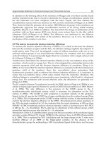
Fig. 23 shows a SEM image of the fabricated pixels. The cathode layer of sub-pixel is
successfully isolated by separator (Fig. 23 (a)). And it is connected with the drain of a-Si:H
TFT through the via hole which is formed by step-covering layer (Fig. 23 (b)).
Fig. 22. Fabrication process flow of a newly proposed normal top-emission OLED pixel
employing cathode-contact structure (a) a-Si:H TFT, (b) reflective anode, (c) step-covering
layer and separator, (d) organic layer evaporation through the shadow mask on the anode,
(e) cathode evaporation.
(a) Top view of CCOLED pixels (b) Cross section of contact area
Fig. 23. SEM image of fabricated cathode-contact type OLED pixel
Organic Light Emitting Diode174
5.3 Electro-optic characteristics
To investigate the pixel performances of the CCTOLED and ACTOLED cells employing the
same TFT and TOLED, we designed and fabricated a unit cell having an emitting area of 1x1
mm
2
. The off current of TFT was about 10
-9
A. The on current, at a gate voltage of 20 V, was
about 10
-3
A at a drain voltage of 10 V resulting in an on-off current ratio of 10
6
. We obtained
a subthreshold slope of approximately 0.74 V/decade demonstrating a sharp device turn-on.
The threshold voltage and the saturation mobility were 1.8 V and 0.34 cm
2
/Vs, respectively.
Fig. 24 shows the current of the OLED (I
OLED
) as a function of the V
DATA
. When the V
SS
was
grounded, the ACTOLED showed lower I
OLED
as compared with the CCTOLED. The I
OLED
of
the ACTOLED and the CCTOLED at V
DATA
= 14 V and V
DD
= 27 V were 1.2 x 10
-4
A and 9.5
x 10
-4
A, respectively.
Fig. 24. Current of the OLED as a function of V
DATA
compared between the ACTOLED and
the CCTOLED
In the case of the ACTOLED, the effective gate voltage (V
GE
) of the driving TFT decreased,
which was defined as the difference of the V
DATA
and the source voltage of the driving TFT
(V
S
) as shown in Fig. 21. The lower current of the ACTOLED was attributed to this lowered-
V
GE
. As a result, the ACTOLED was inappropriate for a high luminance display when the
V
SS
was grounded. When a negative voltage was supplied at the V
SS
in order to increase the
current value in the ACTOLED as shown in Fig. 21, the I
OLED
of the ACTOLED could reach
the same amount as that of the CCTOLED at V
DATA
= 14 V. However the I
OLED
of the
ACOLED at V
DATA
= 0 V, V
DD
= 16 V, and V
SS
= -11 V and the CCOLED at V
DATA
= 0 V, V
DD
= 27 V, and V
SS
= 0 V were 3.4 x 10
-5
A and 3.6 x 10
-8
A, respectively. In the case of the
ACTOLED even though the V
DATA
was set as 0 V, the V
GE
was not zero because the V
S
of the
driving transistor was induced as a negative voltage when the V
SS
was set as a negative
value. The contrast ratio, which means the ratio of the white and black level, is low because
of a leakage light at the black level. On the other hand, the I
OLED
of the CCTOLED
independent of the V
OLED
, this meant that the V
GE
was always equal to the V
DATA
. Therefore,
the CCTOLED was suitable for better image performances having high luminance and
contrast ratio at the same driving conditions. Fig. 25 shows the current density
characteristics of the CCTOLED as a function of the V
DATA
and the V
DD
. Well-saturated
characteristics were shown over V
DD
= 15 V and less than V
DATA
= 10 V which were the
driving condition for real displays.
Fig. 25. Current density of the OLED as a function of V
DD
and V
DATA
6. Conclusion
In this paper, electrical performances and new approaches to increase the stability of a-Si:H
TFT fabricated on a metal foil substrate were reported. A new cathode-contact structure
employing a normal top emitting OLED also was proposed and compared with an anode-
contact structure by experimental data.
76-µm-thick metal foil laminated on the rigid glass plate. On top of this foil, the rough
surface was planarized and the inverted staggered a-Si:H TFT was fabricated at 150°C. The
acrylic polymer as a planarization layer was well matched to a-Si:H TFT fabricated at 150°C.
The a-Si:H TFT of which size was W=30 μm and L=6 μm showed the good electrical
performances. The off current was about 10
-13
A and the on current at gate voltage of 20 V is
about 10
-6
A at a drain voltage of 10 V, resulting in an on-off current ratio of 10
7
. We
obtained a threshold voltage and mobility of 1.0 V and 0.54 cm
2
/Vs, respectively, in the
saturated regime.
The effect of passivation layer on the performances of a-Si:H TFT under mechanical stress
was investigated. The acryl-passivated TFT could endure mechanical stress better than the
SiNx-passivated TFT. However, a larger threshold voltage shift was observed for the acryl-
passivated TFT when a humidity-temperature test was carried out. The hybrid passivation,
which was composed of SiNx and acrylic polymer was proposed. It secured the degradation
of electrical performances under the mechanical stress and somewhat prevented moisture
penetrating into TFT.
We have studied a negative bias effect using the substrate bias without additional circuits to
enable recovery of the degraded drain-current of a driving TFT in 2T1C pixel circuit, which
was fabricated on a metal foil substrate. When V
DD
was grounded and the substrate was
biased as a negative voltage during idle time, the floating gate electrode of the driving
a-Si:H TFT and Pixel Structure for AMOLED on a Flexible Metal Substrate 175
5.3 Electro-optic characteristics
To investigate the pixel performances of the CCTOLED and ACTOLED cells employing the
same TFT and TOLED, we designed and fabricated a unit cell having an emitting area of 1x1
mm
2
. The off current of TFT was about 10
-9
A. The on current, at a gate voltage of 20 V, was
about 10
-3
A at a drain voltage of 10 V resulting in an on-off current ratio of 10
6
. We obtained
a subthreshold slope of approximately 0.74 V/decade demonstrating a sharp device turn-on.
The threshold voltage and the saturation mobility were 1.8 V and 0.34 cm
2
/Vs, respectively.
Fig. 24 shows the current of the OLED (I
OLED
) as a function of the V
DATA
. When the V
SS
was
grounded, the ACTOLED showed lower I
OLED
as compared with the CCTOLED. The I
OLED
of
the ACTOLED and the CCTOLED at V
DATA
= 14 V and V
DD
= 27 V were 1.2 x 10
-4
A and 9.5
x 10
-4
A, respectively.
Fig. 24. Current of the OLED as a function of V
DATA
compared between the ACTOLED and
the CCTOLED
In the case of the ACTOLED, the effective gate voltage (V
GE
) of the driving TFT decreased,
which was defined as the difference of the V
DATA
and the source voltage of the driving TFT
(V
S
) as shown in Fig. 21. The lower current of the ACTOLED was attributed to this lowered-
V
GE
. As a result, the ACTOLED was inappropriate for a high luminance display when the
V
SS
was grounded. When a negative voltage was supplied at the V
SS
in order to increase the
current value in the ACTOLED as shown in Fig. 21, the I
OLED
of the ACTOLED could reach
the same amount as that of the CCTOLED at V
DATA
= 14 V. However the I
OLED
of the
ACOLED at V
DATA
= 0 V, V
DD
= 16 V, and V
SS
= -11 V and the CCOLED at V
DATA
= 0 V, V
DD
= 27 V, and V
SS
= 0 V were 3.4 x 10
-5
A and 3.6 x 10
-8
A, respectively. In the case of the
ACTOLED even though the V
DATA
was set as 0 V, the V
GE
was not zero because the V
S
of the
driving transistor was induced as a negative voltage when the V
SS
was set as a negative
value. The contrast ratio, which means the ratio of the white and black level, is low because
of a leakage light at the black level. On the other hand, the I
OLED
of the CCTOLED
independent of the V
OLED
, this meant that the V
GE
was always equal to the V
DATA
. Therefore,
the CCTOLED was suitable for better image performances having high luminance and
contrast ratio at the same driving conditions. Fig. 25 shows the current density
characteristics of the CCTOLED as a function of the V
DATA
and the V
DD
. Well-saturated
characteristics were shown over V
DD
= 15 V and less than V
DATA
= 10 V which were the
driving condition for real displays.
Fig. 25. Current density of the OLED as a function of V
DD
and V
DATA
6. Conclusion
In this paper, electrical performances and new approaches to increase the stability of a-Si:H
TFT fabricated on a metal foil substrate were reported. A new cathode-contact structure
employing a normal top emitting OLED also was proposed and compared with an anode-
contact structure by experimental data.
76-µm-thick metal foil laminated on the rigid glass plate. On top of this foil, the rough
surface was planarized and the inverted staggered a-Si:H TFT was fabricated at 150°C. The
acrylic polymer as a planarization layer was well matched to a-Si:H TFT fabricated at 150°C.
The a-Si:H TFT of which size was W=30 μm and L=6 μm showed the good electrical
performances. The off current was about 10
-13
A and the on current at gate voltage of 20 V is
about 10
-6
A at a drain voltage of 10 V, resulting in an on-off current ratio of 10
7
. We
obtained a threshold voltage and mobility of 1.0 V and 0.54 cm
2
/Vs, respectively, in the
saturated regime.
The effect of passivation layer on the performances of a-Si:H TFT under mechanical stress
was investigated. The acryl-passivated TFT could endure mechanical stress better than the
SiNx-passivated TFT. However, a larger threshold voltage shift was observed for the acryl-
passivated TFT when a humidity-temperature test was carried out. The hybrid passivation,
which was composed of SiNx and acrylic polymer was proposed. It secured the degradation
of electrical performances under the mechanical stress and somewhat prevented moisture
penetrating into TFT.
We have studied a negative bias effect using the substrate bias without additional circuits to
enable recovery of the degraded drain-current of a driving TFT in 2T1C pixel circuit, which
was fabricated on a metal foil substrate. When V
DD
was grounded and the substrate was
biased as a negative voltage during idle time, the floating gate electrode of the driving
Organic Light Emitting Diode176
transistor was induced as a negative voltage by the dielectric capacitor. The degraded drain
current of the driving transistor can be recovered during the idle time by simply applying a
negative substrate bias. The power consumption can be neglected during the idle time
because no current flows.
Cathode-contact structure pixel structure employing normal TOLED was proposed for a-
Si:H TFT backplane. The new top-emission AMOLED pixel structure employing the TOLED
as well as the cathode-drain contact structure was proposed and fabricated. The structure of
TOLED had a cathode at bottom and an anode on top. The negative photo-resist separator
wall successfully patterned the pixel cathode layers. As the electrical performances of
CCTOLED and ACTOLED were compared, the CCTOLED was verified more suitable for
better display performance having a high luminance and a high contrast ratio.
7. References
Ashtiani, S.,J.; Servati, P.; Striakhilev, D. & Nathan, A. (2005). A 3-TFT Current-Programmed
Pixel Circuit for AMOLEDs. IEEE Trans. Electron Devices, Vol. 52, (July, 2005) 1514-
1518, ISSN 0018-9383
Burrows, E.; Graff, G. L.; Gross, M. E.; Martin, P.M.; Hall, M.; Mast, E.; Bonham, C.; Bennet,
W.; Michalski, M.; Weaver, M. S.; Brown, J. J.; Fogarty, D.& Sapochak, L. S. (2001).
Gas permeation and lifetime tests on polymer-based barrier coatings, Proceedings of
SPIE, pp. 75-83, ISBN 9780819437501, Feb. 2001, Society of photo-optical
Instrumentation Engineers, Bellingham
Chandler, H. H.; Bowen, R. L. & Paffenbarger, G. C. (1971). Physical properties of a
radiopaque denture base material. J. Biomed. Mater. Res., Vol. 5, (July, 1971) 335-357,
ISSN 1549-3296
Chen, C. W.; Lin, C. L. & Wu, C. C. (2004). An effective cathode structure for inverted top-
emitting organic light-emitting devices, Appl. Phys. Lett., Vol. 85, 2469-2471, ISSN
0003-6951
Dobbertin, T.; Werner, O.; Meyer, J.; Kammoun, A.; Schneider, D.; Riedl, T.; Becker, E.;
Johannes, H. H. & Kowalsky, W. (2003). Inverted hybrid organic light-emitting
device with polyethylene dioxythiophene-polystyrene sulfonate as an anode buffer
layer, Appl. Phys. Lett., Vol. 83, 5071-5073, ISSN 0003-6951
Fu, L.; Lever, P.; Tan, H. H.; Jagadish, C.; Reece, P. & Gal, M. (2002). Suppression of
interdiffusion in GaAs/AlGaAs quantum-well structure capped with dielectric
films by deposition of gallium oxide, Appl. Phys. Lett., Vol. 82, 3579-3583, ISSN
0003-6951
Goh, J. C.; Jang, J.; Cho, K. S. & Kim, C. K. (2003). A New a-Si:H Thin-Film Transistor Pixel
Circuit for Active-Matrix Organic Light Emitting Diodes, IEEE Electron Device Lett.,
Vol. 24, 583-585, ISSN 0741-3106
Hicknell, T.,S.; Fliegel, F. M. & Hicknell, F. S. (1990). The Elastic Properties of Thin-Film
Silicon Nitride, Proceedings of IEEE Ultrasonic Symposium, pp. 445-448, Institute of
Electrical & Electronics Enginee
Hiranaka , K.; Yoshimura, T. & Yamaguchi, T. (1989). Effects of the Deposition Sequence on
Amorphous Silicon Thin-Film Transistors, Jpn. J. Appl. Phys., Vol. 28, 2197-2200,
ISSN 0021-4922
Hong, M. P.; Seo, J. H.; Lee, W. J.; Rho, S. G.; Hong, W. S.; Choi, T. Y.; Jeon, H. I.; Kim, S. I.;
Kim, B. S.; Lee, Y. U.; Oh, J. H.; Cho, J. H. & Chung, K. H. (2005) Large Area Full
Color Transmissive a-Si TFT-LCD Using Low Temperature Processes on Plastic
Substrate, Proceedings of SID Symposium, Vol. 36, pp.14-17, Boston, MA, May 2005,
SID, San Jose, CA, ISSN 005-966x
Hong, Y. T.; Heiler, G.; Kerr, R.; Kattamis, A. Z.; Cheng, I. C. & Wagner, S. (2006)
Amorphous Silicon Thin-Film Transistor Backplane on Stainless Steel Foil Substrate
for AMOLEDs, Proceedings of SID Symposium, Vol. 37, pp.1862-1865, San Francisco,
CA, June 2006, SID, San Jose, CA, ISSN 006-966x
Jones, B. L. (1985). The Effect of Mechanical Stress on Amorphous Silicon Transistors, J. Non-
Cryst. Solids, Vol. 77&78, 1405-1408, ISSN 0022-3093
Lee, J. H.; You, B. H.; Han, C. W.; Shin, K. S.& Han, M. K. (2005) A New a-Si:H TFT Pixel
Circuit Suppressing OLED Current Error Caused by the Hysteresis and Threshold
Voltage Shift for Active Matrix Organic Light Emitting Diode, Proceedings of SID
Symposium, Vol. 36, pp. 228-231, Boston, MA, May 2005, SID, San Jose, CA, ISSN
005-966x
Liao, W. S. & Lee, S. C. (1997). Novel Low-Temperature Double Passivation Layer in
Hydrogenated Amorphous Silicon Thin Film Transistors, Jpn. J. Appl. Phys., Vol. 36,
2073-2076, ISSN 0021-4922
Lim, B. C.; Choi, Y. J.; Choi, J. H. & Jang, J. (2000). Hydrogenated Amorphous Silicon Thin
Film Transistor Fabricated on Plasma Treated Silicon Nitride, IEEE Trans. Electron
Device, Vol. 47, 367-371, ISSN 0018-9383
Lin, Y. C.; Shieh, H. P. D. & Kanicki, J. (2005). A Novel Current-Scaling a-Si:H TFTs Pixel
Electrode Circuit for AM-OLEDs, IEEE Trans. Electron Devices, Vol. 52, 1123-1131,
0018-9383
Lustig, N.& Kanicki J. (1989). Gate dielectric and contact effects in hydrogenated
amorphous silicon-silicon nitride thin-film transistors, J. Appl. Phys., Vol. 65, 3951-
3957, ISSN 0003-6951
Park, S. K.; Han, J. I. & Kim, W. K. (2001). Mechanics of indium-tin-oxide films on polymer
substrate with organic buffer layer, Proceedings of Mater. Res. Soc. Symp., Vol. 695,
pp. 223-230, ISBN 1-55899-631-1, Boston, MA, Nov. 2001, MRS, Warrendale, PA.
Stutzmann, M. (1985). Role of mechanical stress in the light-induced degradation of
hydrogenated amorphous silicon, Appl. Phys. Lett., Vol. 47, 21- 23, ISSN 0003-8979
Suo, Z.; Ma, E. Y.; Gleskova, H. & Wagner, S. (1999). Mechanics of rollable and foldable film-
on-foil electronics, Appl. Phys. Lett., Vol. 74, 1177- 1179, ISSN 0003-6951
Tanielian, M.; Fritzsche, H.; Tsai, C. C.& Symbalisty, E. (1978). Effect of adsorbed gases on
the conductance of amorphous films of semiconductor silicon-hydrogen alloys,
Appl. Phys. Lett., Vol. 33, 353 -356, ISSN 0003-6951
Tsujimura, T. (2004). Amorphous/Microcrystalline Silicon Thin Film Transistor
Characteristics for Large Size OLED Television Driving, Jpn. J. Appl. Phys., Vol. 43,
5122-5128, ISSN 0021-4922
Wagner, S.; Cheng, I. C.; Kattamis, A. Z.; Cannella, V. & Hong, Y. T. (2006). Flexible Stainless
Steel Substrates for a-Si Display Backplanes, Proceedings of IDRC Symposium, pp.
13-15, Kent, Ohio, Sep. 2006, SID, San Jose, CA, ISSN 1083-1312
a-Si:H TFT and Pixel Structure for AMOLED on a Flexible Metal Substrate 177
transistor was induced as a negative voltage by the dielectric capacitor. The degraded drain
current of the driving transistor can be recovered during the idle time by simply applying a
negative substrate bias. The power consumption can be neglected during the idle time
because no current flows.
Cathode-contact structure pixel structure employing normal TOLED was proposed for a-
Si:H TFT backplane. The new top-emission AMOLED pixel structure employing the TOLED
as well as the cathode-drain contact structure was proposed and fabricated. The structure of
TOLED had a cathode at bottom and an anode on top. The negative photo-resist separator
wall successfully patterned the pixel cathode layers. As the electrical performances of
CCTOLED and ACTOLED were compared, the CCTOLED was verified more suitable for
better display performance having a high luminance and a high contrast ratio.
7. References
Ashtiani, S.,J.; Servati, P.; Striakhilev, D. & Nathan, A. (2005). A 3-TFT Current-Programmed
Pixel Circuit for AMOLEDs. IEEE Trans. Electron Devices, Vol. 52, (July, 2005) 1514-
1518, ISSN 0018-9383
Burrows, E.; Graff, G. L.; Gross, M. E.; Martin, P.M.; Hall, M.; Mast, E.; Bonham, C.; Bennet,
W.; Michalski, M.; Weaver, M. S.; Brown, J. J.; Fogarty, D.& Sapochak, L. S. (2001).
Gas permeation and lifetime tests on polymer-based barrier coatings, Proceedings of
SPIE, pp. 75-83, ISBN 9780819437501, Feb. 2001, Society of photo-optical
Instrumentation Engineers, Bellingham
Chandler, H. H.; Bowen, R. L. & Paffenbarger, G. C. (1971). Physical properties of a
radiopaque denture base material. J. Biomed. Mater. Res., Vol. 5, (July, 1971) 335-357,
ISSN 1549-3296
Chen, C. W.; Lin, C. L. & Wu, C. C. (2004). An effective cathode structure for inverted top-
emitting organic light-emitting devices, Appl. Phys. Lett., Vol. 85, 2469-2471, ISSN
0003-6951
Dobbertin, T.; Werner, O.; Meyer, J.; Kammoun, A.; Schneider, D.; Riedl, T.; Becker, E.;
Johannes, H. H. & Kowalsky, W. (2003). Inverted hybrid organic light-emitting
device with polyethylene dioxythiophene-polystyrene sulfonate as an anode buffer
layer, Appl. Phys. Lett., Vol. 83, 5071-5073, ISSN 0003-6951
Fu, L.; Lever, P.; Tan, H. H.; Jagadish, C.; Reece, P. & Gal, M. (2002). Suppression of
interdiffusion in GaAs/AlGaAs quantum-well structure capped with dielectric
films by deposition of gallium oxide, Appl. Phys. Lett., Vol. 82, 3579-3583, ISSN
0003-6951
Goh, J. C.; Jang, J.; Cho, K. S. & Kim, C. K. (2003). A New a-Si:H Thin-Film Transistor Pixel
Circuit for Active-Matrix Organic Light Emitting Diodes, IEEE Electron Device Lett.,
Vol. 24, 583-585, ISSN 0741-3106
Hicknell, T.,S.; Fliegel, F. M. & Hicknell, F. S. (1990). The Elastic Properties of Thin-Film
Silicon Nitride, Proceedings of IEEE Ultrasonic Symposium, pp. 445-448, Institute of
Electrical & Electronics Enginee
Hiranaka , K.; Yoshimura, T. & Yamaguchi, T. (1989). Effects of the Deposition Sequence on
Amorphous Silicon Thin-Film Transistors, Jpn. J. Appl. Phys., Vol. 28, 2197-2200,
ISSN 0021-4922
Hong, M. P.; Seo, J. H.; Lee, W. J.; Rho, S. G.; Hong, W. S.; Choi, T. Y.; Jeon, H. I.; Kim, S. I.;
Kim, B. S.; Lee, Y. U.; Oh, J. H.; Cho, J. H. & Chung, K. H. (2005) Large Area Full
Color Transmissive a-Si TFT-LCD Using Low Temperature Processes on Plastic
Substrate, Proceedings of SID Symposium, Vol. 36, pp.14-17, Boston, MA, May 2005,
SID, San Jose, CA, ISSN 005-966x
Hong, Y. T.; Heiler, G.; Kerr, R.; Kattamis, A. Z.; Cheng, I. C. & Wagner, S. (2006)
Amorphous Silicon Thin-Film Transistor Backplane on Stainless Steel Foil Substrate
for AMOLEDs, Proceedings of SID Symposium, Vol. 37, pp.1862-1865, San Francisco,
CA, June 2006, SID, San Jose, CA, ISSN 006-966x
Jones, B. L. (1985). The Effect of Mechanical Stress on Amorphous Silicon Transistors, J. Non-
Cryst. Solids, Vol. 77&78, 1405-1408, ISSN 0022-3093
Lee, J. H.; You, B. H.; Han, C. W.; Shin, K. S.& Han, M. K. (2005) A New a-Si:H TFT Pixel
Circuit Suppressing OLED Current Error Caused by the Hysteresis and Threshold
Voltage Shift for Active Matrix Organic Light Emitting Diode, Proceedings of SID
Symposium, Vol. 36, pp. 228-231, Boston, MA, May 2005, SID, San Jose, CA, ISSN
005-966x
Liao, W. S. & Lee, S. C. (1997). Novel Low-Temperature Double Passivation Layer in
Hydrogenated Amorphous Silicon Thin Film Transistors, Jpn. J. Appl. Phys., Vol. 36,
2073-2076, ISSN 0021-4922
Lim, B. C.; Choi, Y. J.; Choi, J. H. & Jang, J. (2000). Hydrogenated Amorphous Silicon Thin
Film Transistor Fabricated on Plasma Treated Silicon Nitride, IEEE Trans. Electron
Device, Vol. 47, 367-371, ISSN 0018-9383
Lin, Y. C.; Shieh, H. P. D. & Kanicki, J. (2005). A Novel Current-Scaling a-Si:H TFTs Pixel
Electrode Circuit for AM-OLEDs, IEEE Trans. Electron Devices, Vol. 52, 1123-1131,
0018-9383
Lustig, N.& Kanicki J. (1989). Gate dielectric and contact effects in hydrogenated
amorphous silicon-silicon nitride thin-film transistors, J. Appl. Phys., Vol. 65, 3951-
3957, ISSN 0003-6951
Park, S. K.; Han, J. I. & Kim, W. K. (2001). Mechanics of indium-tin-oxide films on polymer
substrate with organic buffer layer, Proceedings of Mater. Res. Soc. Symp., Vol. 695,
pp. 223-230, ISBN 1-55899-631-1, Boston, MA, Nov. 2001, MRS, Warrendale, PA.
Stutzmann, M. (1985). Role of mechanical stress in the light-induced degradation of
hydrogenated amorphous silicon, Appl. Phys. Lett., Vol. 47, 21- 23, ISSN 0003-8979
Suo, Z.; Ma, E. Y.; Gleskova, H. & Wagner, S. (1999). Mechanics of rollable and foldable film-
on-foil electronics, Appl. Phys. Lett., Vol. 74, 1177- 1179, ISSN 0003-6951
Tanielian, M.; Fritzsche, H.; Tsai, C. C.& Symbalisty, E. (1978). Effect of adsorbed gases on
the conductance of amorphous films of semiconductor silicon-hydrogen alloys,
Appl. Phys. Lett., Vol. 33, 353 -356, ISSN 0003-6951
Tsujimura, T. (2004). Amorphous/Microcrystalline Silicon Thin Film Transistor
Characteristics for Large Size OLED Television Driving, Jpn. J. Appl. Phys., Vol. 43,
5122-5128, ISSN 0021-4922
Wagner, S.; Cheng, I. C.; Kattamis, A. Z.; Cannella, V. & Hong, Y. T. (2006). Flexible Stainless
Steel Substrates for a-Si Display Backplanes, Proceedings of IDRC Symposium, pp.
13-15, Kent, Ohio, Sep. 2006, SID, San Jose, CA, ISSN 1083-1312
Organic Light Emitting Diode178
Wehrspohn, R. B.; Deane, S. C.; French, I. D.; Gale, I.; Hewett, J.; Powell, M. J. & Robertson, J.
(2000). Relative importance of the Si–Si bond and Si–H bond for the stability of
amorphous silicon thin film transistors, J. Appl. Phys., Vol. 87, 144-154, ISSN 0021-
8979
Yoon, J. K. & Kim, J. H. (1998). Device Analysis for a-Si:H Thin-Film Transistors with
Organic Passivation Layer, IEEE Electron Device Lett., Vol. 19, 335-337, ISSN 0741-
3106
Organic Light Emitting Diode for White Light Emission 179
Organic Light Emitting Diode for White Light Emission
M.N. Kamalasanan, Ritu Srivastava, Gayatri Chauhan, Arunandan Kumar, Priyanka
Tayagi and Amit Kumar
X
Organic Light Emitting Diode
for White Light Emission
M.N. Kamalasanan, Ritu Srivastava, Gayatri Chauhan,
Arunandan Kumar, Priyanka Tayagi and Amit Kumar
Center for Organic Electronics, Polymeric and Soft Materials Section, National Physical
Laboratory (Council of Scientific and Industrial Research), Dr. K.S. Krishnan Road,
New Delhi 110012, India
1. Introduction
During the last few years, research based on energy saving technologies is being given high
priority all over the world. General lighting is one area in which large quantity of electrical
energy is being spend and substantial energy saving is possible by using energy saving
technologies. Conventional light sources like incandescent filament lamps in which a major
part of the energy is wasted as heat and is a less energy efficient technology is being phased
out. Other technologies like gas filled electrical discharge lamps are more efficient but are
polluting. Therefore there is a need for energy efficient and clean light source and solid state
lighting is one of the ways to address the problem
Organic light emitting diodes (OLED) is a new technology which has the potential to replace
the existing lighting technologies. The attraction to organic semiconductors for lighting and
display application has started during 1950-1960 because of the high fluorescence quantum
efficiency exhibited by some organic molecules and their ability to generate a wide variety
of colors. Study of electroluminescence (EL) in organic semiconductors have started in 1950s
by Bernanose et.al (1953) using dispersed polymer films This was followed by the study of
electroluminescence in anthracene single crystals by Pope et al (1963) and W.Helfrich et.al.
(1965) who has studied the fundamental aspects of light generation in OLEDs. Since the
single crystal based anthracence OLEDs fabricated by Pope et al (1963) were very thick and
worked at very high voltages, the devices were not commercialized. In 1987, Tang and
VanSlyke (1987) of Eastman Kodak has demonstrated a highly efficient multi layer OLED
device based on vacuum evaporated aluminum tris 8-hydroxy quonoline (Alq
3
)as the
emitter material. The device had different layers for hole transporting, electron transporting
and light emission. Transparent Indium Tin Oxide (ITO) and aluminum metal were the
anode and cathode respectively. Quantum efficiency and luminescence efficiency of 1% and
1lm/W respectively were considered enough for commercial application. This work has
stimulated a very intense activity in the field of Organic electroluminescence. Numerous
improvements in device structure and addition of more layers having different
functionalities were incorporated and are now on the verge of commercialization. Further,
the developments in - conjugated polymers by Heeger, MacDiarmid, and Shirakawa in
10
Organic Light Emitting Diode180
1977 for which they shared the 2000 Noble Prize in Chemistry as well as the report by
Burroughes et al. (1990)of the first polymer (long chain molecules) light-emitting diode has
also given a boost to the already expanding field of OLEDs. The new discovery of polymer
light emitting diodes(PLEDs) have shown that even solution grown thin layers of a
conjugated polymer can be used as an emitter material which has given new device
concepts like ink jet printing and roll to roll processing of OLEDs. In 1998, Baldo et al (1998)
showed that the efficiency of OLEDs can be improved by the incorporation of
phosphorescent dyes. In this way, the triplets generated in the electron-hole recombination
process (~75%) which are otherwise not used in light generation can be harvested to get
light emission. This new development has enhanced the internal quantum efficiency of
organic LEDs to nearly 100%. Sun et al (2006) introduced a different device concept that
exploits a blue fluorescent in combination with green and red phosphor dopants, to yield
high power efficiency and stable colour balance, while maintaining the potential for unity
internal quantum efficiency. Two distinct modes of energy transfer within this device serve
to channel nearly all of the triplet energy to the phosphorescent dopants i.e, retaining the
singlet energy exclusively on the blue fluorescent dopant and eliminating the exchange
energy loss to the blue fluorophore by direct excitation which allows for roughly 20 per cent
increased power efficiency compared to a fully phosphorescent device. The device
challenges incandescent sources by exhibiting total external quantum and power efficiencies
that peak at 18.7 +/- 0.5 per cent and 37.6 +/- 0.6 lm/W, respectively, decreasing to 18.4 +/-
0.5 per cent and 23.8 +/- 0.5 lm/W at a high luminance of 500 cd/m
2
.
Further, introduction of new technological concepts like electrical doping of transport layers
has enhanced the OLED efficiency to more than 100 lm/W and enhanced life time of the
devices to more than 100,000 hours which is better than the gas filled discharge lamps
(Murano et al 2005). However, efficiency and lifetime are still considered widely as the big
obstacles on the road of OLED development. A further improvement in the OLED
performance relies on the more detailed understanding of the EL physics and the new
development in the OLED materials, structure and fabrication.
Even though OLEDs of different colours have been developed with enough efficiency for
commercialization, white light emitting organic LEDs have a special significance. It can be
used for general lighting, back light for LED displays and for display applications. Since
Organic materials are band emitters, OLEDs using these materials are mono chromatic and
have low half width. Single broad band emitters developed so far has low efficiencies. To
get white light emission from organic materials special efforts have to be made. Many
methods like optical doping using fluorescent and phosphorescent materials as well as
down conversion using inorganic phosphors have been used to get white light emission.
Compared to other sources, OLEDs are thin, flat, lightweight, flexible and emitts cold light.
WOLED having high energy efficiency of 62 lm/W have been demonstrated on R&D level
by OSRAM Opto Semiconductor GmbH (Nov. 2009) and >100 lm/W reachable in future.
They can produce high quality white light (CRI ~ 80), which are diffuse and non glaring
large area light source. Further, they can be instantly on/off and are driven at low voltages.
They have various colors and different color temperatures functionality.
Numerous white OLEDs have been fabricated (Kido et al 1994, 1996, Dodabalapur et al
1994, Yang et al 1997). In the fabrication of full colour display all three primary colours have
equal importance but white light emission has drawn particular attention because any
desired colour range can be achieved by filtering of white light (Strukeji et al 1996, Zhang et
al 2001). To obtain high quality (high CRI) white light, all the three primary colors red,
green, and blue have to be produced simultaneously. Since it is difficult to obtain all
primary emissions from a single molecule, excitation of more than one organic species is
often necessary, thus introducing color stability problems. Due to the different degradation
rate of the employed organic compounds, the emission color of the device can, in fact,
change with time.
The first white OLED was produced by Kido and his colleagues in 1994. This device
contained red, green and blue light emitting compounds that together produce white light.
But there were some problems with these devices such as their efficiency was less than 1
lm/W, required large driving voltage and burned out quickly. But now the efficiency of
these devices has increased very fast. White emission from OLEDs can now be achieved in
both small molecule and polymer systems (Strukeji et al 1996, Granstom et al 1996, Jordan et
al 1996). The yearly progress in the efficiencies of conventional LEDs, nitride LEDs and
white OLEDs is shown in Fig.1.
Fig. 1. The yearly progress in the efficiencies of conventional LEDs, nitride LEDs and white
OLEDs
Fig. 2. 1”x1” proto type of a multilayer phosphorescent efficient WOLED developed at
National Physical Laboratory, New Delhi, India
Organic Light Emitting Diode for White Light Emission 181
1977 for which they shared the 2000 Noble Prize in Chemistry as well as the report by
Burroughes et al. (1990)of the first polymer (long chain molecules) light-emitting diode has
also given a boost to the already expanding field of OLEDs. The new discovery of polymer
light emitting diodes(PLEDs) have shown that even solution grown thin layers of a
conjugated polymer can be used as an emitter material which has given new device
concepts like ink jet printing and roll to roll processing of OLEDs. In 1998, Baldo et al (1998)
showed that the efficiency of OLEDs can be improved by the incorporation of
phosphorescent dyes. In this way, the triplets generated in the electron-hole recombination
process (~75%) which are otherwise not used in light generation can be harvested to get
light emission. This new development has enhanced the internal quantum efficiency of
organic LEDs to nearly 100%. Sun et al (2006) introduced a different device concept that
exploits a blue fluorescent in combination with green and red phosphor dopants, to yield
high power efficiency and stable colour balance, while maintaining the potential for unity
internal quantum efficiency. Two distinct modes of energy transfer within this device serve
to channel nearly all of the triplet energy to the phosphorescent dopants i.e, retaining the
singlet energy exclusively on the blue fluorescent dopant and eliminating the exchange
energy loss to the blue fluorophore by direct excitation which allows for roughly 20 per cent
increased power efficiency compared to a fully phosphorescent device. The device
challenges incandescent sources by exhibiting total external quantum and power efficiencies
that peak at 18.7 +/- 0.5 per cent and 37.6 +/- 0.6 lm/W, respectively, decreasing to 18.4 +/-
0.5 per cent and 23.8 +/- 0.5 lm/W at a high luminance of 500 cd/m
2
.
Further, introduction of new technological concepts like electrical doping of transport layers
has enhanced the OLED efficiency to more than 100 lm/W and enhanced life time of the
devices to more than 100,000 hours which is better than the gas filled discharge lamps
(Murano et al 2005). However, efficiency and lifetime are still considered widely as the big
obstacles on the road of OLED development. A further improvement in the OLED
performance relies on the more detailed understanding of the EL physics and the new
development in the OLED materials, structure and fabrication.
Even though OLEDs of different colours have been developed with enough efficiency for
commercialization, white light emitting organic LEDs have a special significance. It can be
used for general lighting, back light for LED displays and for display applications. Since
Organic materials are band emitters, OLEDs using these materials are mono chromatic and
have low half width. Single broad band emitters developed so far has low efficiencies. To
get white light emission from organic materials special efforts have to be made. Many
methods like optical doping using fluorescent and phosphorescent materials as well as
down conversion using inorganic phosphors have been used to get white light emission.
Compared to other sources, OLEDs are thin, flat, lightweight, flexible and emitts cold light.
WOLED having high energy efficiency of 62 lm/W have been demonstrated on R&D level
by OSRAM Opto Semiconductor GmbH (Nov. 2009) and >100 lm/W reachable in future.
They can produce high quality white light (CRI ~ 80), which are diffuse and non glaring
large area light source. Further, they can be instantly on/off and are driven at low voltages.
They have various colors and different color temperatures functionality.
Numerous white OLEDs have been fabricated (Kido et al 1994, 1996, Dodabalapur et al
1994, Yang et al 1997). In the fabrication of full colour display all three primary colours have
equal importance but white light emission has drawn particular attention because any
desired colour range can be achieved by filtering of white light (Strukeji et al 1996, Zhang et
al 2001). To obtain high quality (high CRI) white light, all the three primary colors red,
green, and blue have to be produced simultaneously. Since it is difficult to obtain all
primary emissions from a single molecule, excitation of more than one organic species is
often necessary, thus introducing color stability problems. Due to the different degradation
rate of the employed organic compounds, the emission color of the device can, in fact,
change with time.
The first white OLED was produced by Kido and his colleagues in 1994. This device
contained red, green and blue light emitting compounds that together produce white light.
But there were some problems with these devices such as their efficiency was less than 1
lm/W, required large driving voltage and burned out quickly. But now the efficiency of
these devices has increased very fast. White emission from OLEDs can now be achieved in
both small molecule and polymer systems (Strukeji et al 1996, Granstom et al 1996, Jordan et
al 1996). The yearly progress in the efficiencies of conventional LEDs, nitride LEDs and
white OLEDs is shown in Fig.1.
Fig. 1. The yearly progress in the efficiencies of conventional LEDs, nitride LEDs and white
OLEDs
Fig. 2. 1”x1” proto type of a multilayer phosphorescent efficient WOLED developed at
National Physical Laboratory, New Delhi, India
Organic Light Emitting Diode182
National Physical Laboratory New Delhi has taken up a program for developing WOLEDs
for general lighting applications. In this effort a 1”x1” proto type of a multilayer
phosphorescent efficient WOLED has been demonstrated (Fig.2). In this review, we like to
highlight on the development of white organic LEDs for general lighting.
2. Basic OLED Structure and Operation principles
White organic light emitting diodes are thin-film multilayer devices in which active charge
transport and light emitting materials are sandwiched between two thin film electrodes, and
at least one of the two electrodes must be transparent to light. Generally high work function
(∼4.8 eV), low sheet resistant (20 /□) and optically transparent indium tin oxide (ITO) is
used as an anode, while the cathode is a low work function metal such as Ca, Mg, Al or their
alloys Mg:Ag, Li:Al. An organic layer with good electron transport and hole blocking
properties is typically used between the cathode and the emissive layer. The device
structure of an OLED is given in Fig. 3. When an electric field is applied across the
electrodes, electrons and holes are injected into states of the lowest unoccupied molecular
orbital (LUMO) and the highest occupied molecular orbital (HOMO), respectively and
transported through the organic layer. Inside the semiconductor electrons and holes
recombine to form excited state of the molecule. Light emission from the organic material
occurs when the molecule relaxes from the excited state to the ground state. Highly efficient
OLEDs which are being developed at present, contains many layers with different
functionality like hole injection layer(HIL), hole transport layer (HTL),electron blocking
layer(EBL), emissive layer(EML), hole blocking layer(HBL), electron transport layer(ETL)
and electron injection layer(EIL) etc apart from electrodes. A schematic diagram of
multilayer structure is shown in Fig. 4.
Fig. 3. The device structure of an OLED
Fig. 4. A schematic diagram of multilayer structure of OLED
3. Characterization of White OLEDs
3.1 Colour quality
In order for a light-emitting device to be acceptable as a general illumination source, it
clearly must provide high-illumination-quality light source. White light has three
characteristics (i) the Commission International d’Eclairage (CIE) coordinates (ii) the co
related colour temperature (CCT) and (iii) the colour rendering index (CRI)
3.1.1 Commission International d’Eclairage (C-I-E) co ordinates
The color of a light source is typically characterized in terms of CIE colorimetry system. Any
colour can be expressed by the chromaticity coordinates x and y on the CIE chromaticity
diagram (Fig. 5). The boundaries of this horseshoe-shaped diagram are the plots of
monochromatic light, called spectrum loci, and all the colours in the visible spectrum fall
within or on the boundary of this diagram. The arc near the centre of the diagram is called
the Planckian locus, which is the plot of the coordinates of black body radiation at the
temperatures from 1000 K to 20 000 K, described as CCT. The colours of most of the
traditional light sources fall in the region between 2850 and 6500 K of black body. For
general illumination a light source should have high-energy efficiency and CIE-1931
chromaticity coordinates (x, y) close to the equal energy white (EEW) (0.33, 0.33).
Organic Light Emitting Diode for White Light Emission 183
National Physical Laboratory New Delhi has taken up a program for developing WOLEDs
for general lighting applications. In this effort a 1”x1” proto type of a multilayer
phosphorescent efficient WOLED has been demonstrated (Fig.2). In this review, we like to
highlight on the development of white organic LEDs for general lighting.
2. Basic OLED Structure and Operation principles
White organic light emitting diodes are thin-film multilayer devices in which active charge
transport and light emitting materials are sandwiched between two thin film electrodes, and
at least one of the two electrodes must be transparent to light. Generally high work function
(∼4.8 eV), low sheet resistant (20 /□) and optically transparent indium tin oxide (ITO) is
used as an anode, while the cathode is a low work function metal such as Ca, Mg, Al or their
alloys Mg:Ag, Li:Al. An organic layer with good electron transport and hole blocking
properties is typically used between the cathode and the emissive layer. The device
structure of an OLED is given in Fig. 3. When an electric field is applied across the
electrodes, electrons and holes are injected into states of the lowest unoccupied molecular
orbital (LUMO) and the highest occupied molecular orbital (HOMO), respectively and
transported through the organic layer. Inside the semiconductor electrons and holes
recombine to form excited state of the molecule. Light emission from the organic material
occurs when the molecule relaxes from the excited state to the ground state. Highly efficient
OLEDs which are being developed at present, contains many layers with different
functionality like hole injection layer(HIL), hole transport layer (HTL),electron blocking
layer(EBL), emissive layer(EML), hole blocking layer(HBL), electron transport layer(ETL)
and electron injection layer(EIL) etc apart from electrodes. A schematic diagram of
multilayer structure is shown in Fig. 4.
Fig. 3. The device structure of an OLED
Fig. 4. A schematic diagram of multilayer structure of OLED
3. Characterization of White OLEDs
3.1 Colour quality
In order for a light-emitting device to be acceptable as a general illumination source, it
clearly must provide high-illumination-quality light source. White light has three
characteristics (i) the Commission International d’Eclairage (CIE) coordinates (ii) the co
related colour temperature (CCT) and (iii) the colour rendering index (CRI)
3.1.1 Commission International d’Eclairage (C-I-E) co ordinates
The color of a light source is typically characterized in terms of CIE colorimetry system. Any
colour can be expressed by the chromaticity coordinates x and y on the CIE chromaticity
diagram (Fig. 5). The boundaries of this horseshoe-shaped diagram are the plots of
monochromatic light, called spectrum loci, and all the colours in the visible spectrum fall
within or on the boundary of this diagram. The arc near the centre of the diagram is called
the Planckian locus, which is the plot of the coordinates of black body radiation at the
temperatures from 1000 K to 20 000 K, described as CCT. The colours of most of the
traditional light sources fall in the region between 2850 and 6500 K of black body. For
general illumination a light source should have high-energy efficiency and CIE-1931
chromaticity coordinates (x, y) close to the equal energy white (EEW) (0.33, 0.33).
Organic Light Emitting Diode184
Fig. 5. CIE (x, y) chromaticity diagram.
3.1.2 Colour rendering index (CRI)
For a given light source, the CRI attempts to quantify how different a set of test colors
appears when illuminated by the source compared to when the same test colors are
illuminated by the standard illuminant with the same correlated color temperature. It is
measured in 0-100 scales and the highest possible CRI value is 100, and this occurs when
there is no difference in color rendering between the light source and the standard
illuminant. An example of such a light source is the incandescent lamp. When a color
rendering difference exists, the CRI is less than 100. Achieving illumination-quality white
light generally requires a CRI value of 80 or greater.
3.1.3 Correlated colour temperature (CCT)
The color of a light source is typically characterized in terms of its color temperature. If the
x,y coordinates of an illumination source do not exactly sit on the blackbody locus, the color
of a light source is characterized in terms of its CCT. The CCT is the temperature of a
blackbody radiator that has a colour that most closely matches the emission from a non-
blackbody radiator. For high quality white light illumination the CCT should between
2500K and 6500 K. There is an accepted method (Wyszelki et al 1982) to determine lines of
constant correlated color temperature in x, y space. CIE, CCT and CRI for common white
light sources are given in Table 1 for comparison purpose (Misra et al 2006).
Table 1. Chromaticity coordinates (CIE), correlated colour temperature (CCT) and colour
rendering indices (CRI) for common white light sources.
3.2 Device Efficiency
The efficiency of OLEDs is characterized by quantum efficiency, power efficiency and
luminous efficiency. Over the past several years, the power (η
p
) and external quantum (η
ext
)
efficiencies of white OLEDs have been steadily improving.
3.2.1 Quantum efficiency.
The quantum efficiency of a device can be differentiated into two categories i.e internal and
external quantum efficiencies.
Internal quantum efficiency (IQE)- This is the total number of photons generated inside the
device per electron– hole pair injected into the device. It is represented by η
int
.
For OLEDs the internal quantum efficiency in the case of fluorescent materials is given by
(OIDA 2002)
η
int
= γ η
s
f
, (1)
where γ is the fraction of injected charges that produce excitons and is called the charge
balance factor, η
s
is the fraction of singlet excitons called singlet exciton efficiency and
f
is
the fraction of energy released from material as light and called the quantum efficiency of
fluorescence.
Generally based on spin statistics fluorescent organic materials exhibit 25% singlet and 75%
triplet states in EL and 100% singlet states in PL (Baldo et al 1998, Friend et al 1999). In
fluorescent materials triplet energy states have a low emission quantum yield and thus do
not contribute to electroluminescence. This means the quantum efficiency for EL can only be
about 25% of the PL efficiency. But some organometallic complexes (phosphors) have a
strong triplet emission quantum yield and provide the possibility of a high efficiency EL
device by using these materials. A research group from Princeton University demonstrated
the efficiency limitation breakthrough in OLEDs by energy transfer from fluorescent host to
a phosphorescent guest material (Baldo et al 1998). The phosphorescent dopants are doped
in host materials with a wide energy gap. In electrophosphorescence the energy from both
the singlet and triplet states of the fluorescent host is transferred to the triplet state of the
phosphorescent guest molecule or the charges are directly trapped to the phosphor triplet.
This harvesting of both singlet and triplet states has been resulted result in 100% internal
Organic Light Emitting Diode for White Light Emission 185
Fig. 5. CIE (x, y) chromaticity diagram.
3.1.2 Colour rendering index (CRI)
For a given light source, the CRI attempts to quantify how different a set of test colors
appears when illuminated by the source compared to when the same test colors are
illuminated by the standard illuminant with the same correlated color temperature. It is
measured in 0-100 scales and the highest possible CRI value is 100, and this occurs when
there is no difference in color rendering between the light source and the standard
illuminant. An example of such a light source is the incandescent lamp. When a color
rendering difference exists, the CRI is less than 100. Achieving illumination-quality white
light generally requires a CRI value of 80 or greater.
3.1.3 Correlated colour temperature (CCT)
The color of a light source is typically characterized in terms of its color temperature. If the
x,y coordinates of an illumination source do not exactly sit on the blackbody locus, the color
of a light source is characterized in terms of its CCT. The CCT is the temperature of a
blackbody radiator that has a colour that most closely matches the emission from a non-
blackbody radiator. For high quality white light illumination the CCT should between
2500K and 6500 K. There is an accepted method (Wyszelki et al 1982) to determine lines of
constant correlated color temperature in x, y space. CIE, CCT and CRI for common white
light sources are given in Table 1 for comparison purpose (Misra et al 2006).
Table 1. Chromaticity coordinates (CIE), correlated colour temperature (CCT) and colour
rendering indices (CRI) for common white light sources.
3.2 Device Efficiency
The efficiency of OLEDs is characterized by quantum efficiency, power efficiency and
luminous efficiency. Over the past several years, the power (η
p
) and external quantum (η
ext
)
efficiencies of white OLEDs have been steadily improving.
3.2.1 Quantum efficiency.
The quantum efficiency of a device can be differentiated into two categories i.e internal and
external quantum efficiencies.
Internal quantum efficiency (IQE)- This is the total number of photons generated inside the
device per electron– hole pair injected into the device. It is represented by η
int
.
For OLEDs the internal quantum efficiency in the case of fluorescent materials is given by
(OIDA 2002)
η
int
= γ η
s
f
, (1)
where γ is the fraction of injected charges that produce excitons and is called the charge
balance factor, η
s
is the fraction of singlet excitons called singlet exciton efficiency and
f
is
the fraction of energy released from material as light and called the quantum efficiency of
fluorescence.
Generally based on spin statistics fluorescent organic materials exhibit 25% singlet and 75%
triplet states in EL and 100% singlet states in PL (Baldo et al 1998, Friend et al 1999). In
fluorescent materials triplet energy states have a low emission quantum yield and thus do
not contribute to electroluminescence. This means the quantum efficiency for EL can only be
about 25% of the PL efficiency. But some organometallic complexes (phosphors) have a
strong triplet emission quantum yield and provide the possibility of a high efficiency EL
device by using these materials. A research group from Princeton University demonstrated
the efficiency limitation breakthrough in OLEDs by energy transfer from fluorescent host to
a phosphorescent guest material (Baldo et al 1998). The phosphorescent dopants are doped
in host materials with a wide energy gap. In electrophosphorescence the energy from both
the singlet and triplet states of the fluorescent host is transferred to the triplet state of the
phosphorescent guest molecule or the charges are directly trapped to the phosphor triplet.
This harvesting of both singlet and triplet states has been resulted result in 100% internal
Organic Light Emitting Diode186
quantum efficiency (Adachi et al 2001). But exciton–exciton quenching (Baldo et al 2000),
polaron– exciton quenching (Young et al 2002) and exciton dissociation (Szmytkowski et al
2002) may reduce the internal quantum efficiency to much lower values.
One of the important developments of WOLEDs is the demonstration of phosphorescence
sensitization of EL (Kanno et al 2006). It has been observed that addition of a small quantity
of a phosphorescent dopant in a guest host system enhances the fluorescence efficiency of a
co-dopant. Cheng et al (2003) reported that the internal efficiency of fluorescence can be
enhanced to 100% by using a phosphorescent sensitizer to excite the fluorescent dye through
resonant energy transfer between the triplet excitons in the phosphor and singlets in the
fluorescent dye. Using the blue emission from a spatially separated hole transport layer NPB
and Ir(ppy)
3
sensitized DCJTB in a CBP host the authors obtained the high efficiency white
OLEDs. The colour tuning has been achieved by varying the concentration of the sensitizer
as well as the thickness of the co-doped emitter layer.
External quantum efficiency (EQE)- This is defined as the total number of photons emitted
from the device per electron–hole pair injected into the device. It is represented by η
ext
.
The external quantum efficiency is related to the internal quantum efficiency and is given by
(OIDA 2002)
η
ext
= R
e
η
int
, (2)
where R
e
is the extraction or outcoupling efficiency representing the number of photons
emitted from the device per number of photons generated in the device.
3.2.2 Power Efficiency
The luminous efficacy or power efficiency is the lumen output per input electrical power of
the device. It is measured in lumen per watt (lm/ W) or candela per ampere (cd/ A). It is
represented by η
p
. In order to compete with the fluorescent lighting market, the efficiency of
OLED sources should be 120 lm/ W or more. To meet the above requirement the OLED
sources must have an electrical to optical power conversion efficiency of 34%. For white
light with a CRI of 90 the maximum value is 408 lm/W and for a CRI of 100 it is 240 lm/W
(Kamtekar 2010).
The projection for WOLED is that by 2015, efficiency will exceed 100 lm/W with desirable
life time and brightness and will start to replace indoor and outdoor light. Murano et al
demonstrated white pin-OLEDs based on phosphorescent and fluorescent emitters and
stacked OLEDs. This intentional doping of the transport layer led to a very high power
efficiency of well above 20 lm/W at 1000 cd/m
2
(Murano et al 2005). The CRI properties of
emitted light are very high, between 85 and 95. Universal Display Corporation (UDC)
announced the demonstration of a white OLED lighting panel with a high power efficiency
of 30 lm/ W using the company’s phosphorescent OLED technology. This efficiency was
achieved at a colour temperature of 4000 K, which is comparable to the colour temperature
and power efficiency of a cool fluorescent lamp. The colour-rendering index was >80 across
the measured colour temperatures because of the broad spectral output of the combined
colours. D’Andrade et al (2004) reported power efficiency of 42 lm/ W for a white OLED
that exceeds that of incandescent lamps. Therefore WOLEDs have great potential for energy
saving and the replacement of traditional incandescent light sources.
3.2.3 Improvement of Efficiency
One of the measure problems in OLEDs is its low efficiency. Various techniques are used to
improve the efficiency of OLED devices.
3.2.3.1 Triplet Harvesting
Due to spin statistics the efficiencies of OLEDs are limited, as only the singlets are
responsible for light emission in EL in undoped devices. The recent developments in
harvesting of triplet states, using phosphorescent materials, led to an increase in the
efficiency and selectivity of colours. Electrophosphorescence achieved by doping an
organometallic phosphor into a host has been successfully used for generating the primary
colours necessary for display applications (Baldo et al 1998, Holmes et al 2003, Adachi et al
2001). Due to extensive work, the power efficiency of white organic light emitting devices
(WOLEDs) has continuously increased over the past decade and it has attained the level
required for WOLEDs acceptance into the lighting market. Universal Display Corporation is
a world leader in developing and commercializing innovative OLED technologies and
materials for use in the electronic flat panel display and other markets. Universal Display is
working with a network of world-class organizations including Princeton University, the
University of Southern California, DuPont Displays, Samsung SDI Co., Seiko Epson
Corporation, Sony Corporation, Tohoku Pioneer Corporation and Toyota Industries
Corporation. NOVALED GmbH, Dresden Germany, is another emerging company in the
field of organic displays. NOVALED works in close cooperation with Technical University
Dresden and Fraunhofer Dresden Institute IPMS. According to a press release in 2005 from
Dresden, Germany, NOVALED has developed a green emitting OLED with efficiency of 110
lm /W.
3.2.3.2 Optical doping
The doping of the emissive layer in an OLED has been used extensively as a way of
improving efficiency and lifetime, in addition to being used to modify the emission color
(Optical doping has been explained in guest host system). Tang et al. (1989) first introduced
fluorescent dyes, 3-(2-benzothiazolyl)-7-diethylaminocoumarin (coumarin 540 or coumarin
6 and DCMs, as dopants in Alq
3
to improve the efficiency and color purity of devices. Since
then, a wide range of fluorescent dopants have been used in OLEDs (Sano et al 1997,
Hamada et al 1995). The ground state of most materials has a single spin state. Emission of a
photon in fluorescent materials conserves spin, therefore only singlet excited states typically
emit light. Decay from the triplet excited states is typically a nonradiative process for most
organic materials and so these triplet excitons are lost from the perspective of light emission.
The maximum possible internal quantum efficiency that can be obtained in an OLED using
fluorescent material is limited by the ratio of these excited states or the so-called exciton
singlet-to-triplet ratio, which is approximately 1:3 (Baldo et al 1999, 1999a). This limits
fluorescent OLEDs to a maximum internal quantum efficiency of approximately 25%.
3.2.3.3 Electrical doping
In typical OLEDs, the applied voltage (V) is usually 5–8 V, when illuminated at 500–1000
cd/ m
2
, i.e., greater than twice the voltage of the emitted photon Vg. The voltage drop
across the emission layer itself is usually 2 to 3 V, depending upon the emission wavelength.
Organic Light Emitting Diode for White Light Emission 187
quantum efficiency (Adachi et al 2001). But exciton–exciton quenching (Baldo et al 2000),
polaron– exciton quenching (Young et al 2002) and exciton dissociation (Szmytkowski et al
2002) may reduce the internal quantum efficiency to much lower values.
One of the important developments of WOLEDs is the demonstration of phosphorescence
sensitization of EL (Kanno et al 2006). It has been observed that addition of a small quantity
of a phosphorescent dopant in a guest host system enhances the fluorescence efficiency of a
co-dopant. Cheng et al (2003) reported that the internal efficiency of fluorescence can be
enhanced to 100% by using a phosphorescent sensitizer to excite the fluorescent dye through
resonant energy transfer between the triplet excitons in the phosphor and singlets in the
fluorescent dye. Using the blue emission from a spatially separated hole transport layer NPB
and Ir(ppy)
3
sensitized DCJTB in a CBP host the authors obtained the high efficiency white
OLEDs. The colour tuning has been achieved by varying the concentration of the sensitizer
as well as the thickness of the co-doped emitter layer.
External quantum efficiency (EQE)- This is defined as the total number of photons emitted
from the device per electron–hole pair injected into the device. It is represented by η
ext
.
The external quantum efficiency is related to the internal quantum efficiency and is given by
(OIDA 2002)
η
ext
= R
e
η
int
, (2)
where R
e
is the extraction or outcoupling efficiency representing the number of photons
emitted from the device per number of photons generated in the device.
3.2.2 Power Efficiency
The luminous efficacy or power efficiency is the lumen output per input electrical power of
the device. It is measured in lumen per watt (lm/ W) or candela per ampere (cd/ A). It is
represented by η
p
. In order to compete with the fluorescent lighting market, the efficiency of
OLED sources should be 120 lm/ W or more. To meet the above requirement the OLED
sources must have an electrical to optical power conversion efficiency of 34%. For white
light with a CRI of 90 the maximum value is 408 lm/W and for a CRI of 100 it is 240 lm/W
(Kamtekar 2010).
The projection for WOLED is that by 2015, efficiency will exceed 100 lm/W with desirable
life time and brightness and will start to replace indoor and outdoor light. Murano et al
demonstrated white pin-OLEDs based on phosphorescent and fluorescent emitters and
stacked OLEDs. This intentional doping of the transport layer led to a very high power
efficiency of well above 20 lm/W at 1000 cd/m
2
(Murano et al 2005). The CRI properties of
emitted light are very high, between 85 and 95. Universal Display Corporation (UDC)
announced the demonstration of a white OLED lighting panel with a high power efficiency
of 30 lm/ W using the company’s phosphorescent OLED technology. This efficiency was
achieved at a colour temperature of 4000 K, which is comparable to the colour temperature
and power efficiency of a cool fluorescent lamp. The colour-rendering index was >80 across
the measured colour temperatures because of the broad spectral output of the combined
colours. D’Andrade et al (2004) reported power efficiency of 42 lm/ W for a white OLED
that exceeds that of incandescent lamps. Therefore WOLEDs have great potential for energy
saving and the replacement of traditional incandescent light sources.
3.2.3 Improvement of Efficiency
One of the measure problems in OLEDs is its low efficiency. Various techniques are used to
improve the efficiency of OLED devices.
3.2.3.1 Triplet Harvesting
Due to spin statistics the efficiencies of OLEDs are limited, as only the singlets are
responsible for light emission in EL in undoped devices. The recent developments in
harvesting of triplet states, using phosphorescent materials, led to an increase in the
efficiency and selectivity of colours. Electrophosphorescence achieved by doping an
organometallic phosphor into a host has been successfully used for generating the primary
colours necessary for display applications (Baldo et al 1998, Holmes et al 2003, Adachi et al
2001). Due to extensive work, the power efficiency of white organic light emitting devices
(WOLEDs) has continuously increased over the past decade and it has attained the level
required for WOLEDs acceptance into the lighting market. Universal Display Corporation is
a world leader in developing and commercializing innovative OLED technologies and
materials for use in the electronic flat panel display and other markets. Universal Display is
working with a network of world-class organizations including Princeton University, the
University of Southern California, DuPont Displays, Samsung SDI Co., Seiko Epson
Corporation, Sony Corporation, Tohoku Pioneer Corporation and Toyota Industries
Corporation. NOVALED GmbH, Dresden Germany, is another emerging company in the
field of organic displays. NOVALED works in close cooperation with Technical University
Dresden and Fraunhofer Dresden Institute IPMS. According to a press release in 2005 from
Dresden, Germany, NOVALED has developed a green emitting OLED with efficiency of 110
lm /W.
3.2.3.2 Optical doping
The doping of the emissive layer in an OLED has been used extensively as a way of
improving efficiency and lifetime, in addition to being used to modify the emission color
(Optical doping has been explained in guest host system). Tang et al. (1989) first introduced
fluorescent dyes, 3-(2-benzothiazolyl)-7-diethylaminocoumarin (coumarin 540 or coumarin
6 and DCMs, as dopants in Alq
3
to improve the efficiency and color purity of devices. Since
then, a wide range of fluorescent dopants have been used in OLEDs (Sano et al 1997,
Hamada et al 1995). The ground state of most materials has a single spin state. Emission of a
photon in fluorescent materials conserves spin, therefore only singlet excited states typically
emit light. Decay from the triplet excited states is typically a nonradiative process for most
organic materials and so these triplet excitons are lost from the perspective of light emission.
The maximum possible internal quantum efficiency that can be obtained in an OLED using
fluorescent material is limited by the ratio of these excited states or the so-called exciton
singlet-to-triplet ratio, which is approximately 1:3 (Baldo et al 1999, 1999a). This limits
fluorescent OLEDs to a maximum internal quantum efficiency of approximately 25%.
3.2.3.3 Electrical doping
In typical OLEDs, the applied voltage (V) is usually 5–8 V, when illuminated at 500–1000
cd/ m
2
, i.e., greater than twice the voltage of the emitted photon Vg. The voltage drop
across the emission layer itself is usually 2 to 3 V, depending upon the emission wavelength.
Organic Light Emitting Diode188
The remaining voltage is dropped predominantly across the ETL, across the HTL, and at the
heterojunction interfaces. Charge transport in low-mobility organic films is space-charge
limited (Marks et al 1993) and high electric fields are required to inject the necessary charge
to generate the desired photon flux. Band misalignments at the heterojunction interfaces
also result in voltage loss. However, the drive voltage can be significantly reduced by
electrical doping of the transport layers (Blochwitz 2002). Electrical doping was
demonstrated using green Ir(ppy)
3
-doped PHOLEDs by Pfeiffer et al (2002). It was observed
that the drive voltage necessary to produce 100 cd/ m
2
was 2.65 V, i.e., only slightly higher
than Vg. This device used p-type (tetra fluoro tetra cyano quino dimethane (F
4
-TCNQ)) and
n-type (Li) doping of the HTL and ETL, respectively. In this effort Murano et al from
NOVALED demonstrated efficient white OLEDs based on an intentional doping of the
charge carrier transport layers and the usage of different state of the art emission principles
(Murano et al 2005).
Large quantity of (~50%) low work function metal like Li is usually co-evaporated with
conventional electron transport materials like Bphen to achieve n-type doping. In
corporation of low work function metals induces stability problems in OLEDs. Recently
Tyagi et al (2010) have demonstrated efficient n-type doping by doping Liq in electron
transport material Alq
3
. An increase in current density by two orders of magnitude has been
achieved with 33 wt% of Liq doped in Alq
3
. Organic light emitting diode with p–i–n
structure was fabricated using F
4
-TCNQ doped -NPD as hole transport layer, Ir(ppy)
3
doped CBP as emitting layer and 33 wt% Liq doped Alq
3
as electron transport layer.
Comparison of OLEDs fabricated using undoped Alq
3
and 33 wt% Liq doped Alq
3
as
electron transport layer shows reduction in turn on voltage from 5 to 2.5V and enhancement
of power efficiency from 5.8 to 10.6 lm/W at 5V.
3.2.3.4 Improving out coupling efficiency
It is well understood that the generated light from the active OLED medium propagates via
various modes, that is, external modes (escape from the substrate surface), substrate-, and
ITO/organic-waveguided modes due to total internal reflection (TIR) (Gu et al 1997,
Madigan 2000, Moller and Forrest 2002). According to the ray optics theory, about 80% of
the generated light is lost in waveguided modes due to glass substrate and ITO/organic
material which means that the majority of generated light is either trapped inside the glass
substrate and device, or emitted out from the edges of an OLED (Gu et al 1997, Madigan
2000, Moller and Forrest 2002). For the purpose of applications in general illumination and
flat panel displays, light emitted from the substrate surface (external modes) is most useful
which is only about 20% of the total emitted light from the OLED.
Detailed optical modelling (Kim et al 2000) predicted that the fraction of the light emitted in
the forward direction is reduced by a factor of (4/3)n
2
, where n is the index of refraction of
the emitter layer. Through a series of experiments using an integrating sphere, Cao et al
(Cao et al 1999) demonstrated that the measured reduction factor is approximately 2–2.5,
less than the theoretical value 2n
2
∼ 6. Forrest and coworkers found that the total external
efficiency is larger by a factor of 1.7–2.3 than observed in the forward viewing direction
(D’Andrade et al 2004). The poor light extraction is the most important factor which limits
the external quantum efficiency of devices and hence better outcoupling methods are to be
developed to get higher efficiencies. To extract the trapped and waveguided light into
external modes, various approaches based on light refraction and scattering to reduce TIR at
the interfaces have been reported, such as, the use of a shaped substrate (Gu et al
1997,Madigan et al 2000), use of micro-lenses on the backside of substrate surface (Moller et
al 2002, Peng et al 2005, Lim et al 2006), formation of mono-layer of silica micro-spheres as
scattering medium (Yamasaki et al 2000, Neyts and Nieto 2006), and use of high refractive
index substrate (Lu et al 2000). In another approach, an extremely low refractive index silica-
aerogel layer (Tsutsui et al 2001) was inserted between the ITO transparent electrode and
glass substrate.
A 50% light extraction efficiency from OLEDs was recently reported by insertion of a two-
dimensional photonic crystal structure (Do et al 2004, Kitamura et al 2005, Liu et al 2005, Lee
et al 2005), and using nano-porous and nano-patterned films (Lee et al 2003, Kim et al 2005).
More recently, use of diffusive layer lamination (Nakamura et al 2004), holographic
technique (Liu et al 2005), and shaped substrate OLED luminair (Andrade et al 2006) has
also been investigated for the improvement of out-coupling efficiency in conventional
OLEDs. An index-matching layer has also been used for top emitting OLED (Hung et al
2001).
To extract the trapped light, Saxena et al (2008) used simple AR coating technique and
demonstrated pronounced enhancement in light out-coupling of conventional OLED.
Single-layer MgF
2
was coated on backside of glass substrate of conventional OLED with
thickness of λ/4. About two-fold enhancement in luminance with anti-reflection coating of
MgF
2
has been observed. Fig. 6 shows the schematic diagram of the phenomenon of anti-
reflection (AR) coating using single-layer MgF2 for the extraction of substrate-waveguided
modes.
Fig. 6 Schematic diagram of the phenomenon of anti-reflection (AR) coating using single-
layer MgF
2
for the extraction of substrate-waveguided modes.
3.3 Stability
One issue that limited the early adoption of OLEDs in commercial products was device
stability both during storage and in operation. Suggested causes of degradation include
indium migration from the ITO anode (Lee et al 1999), morphological instability of the
organic materials (Higginson et al 1998), fixed charge accumulation within the device
(Kondakov et al 2003), damage to the electrodes, and the formation of non emissive dark
Organic Light Emitting Diode for White Light Emission 189
The remaining voltage is dropped predominantly across the ETL, across the HTL, and at the
heterojunction interfaces. Charge transport in low-mobility organic films is space-charge
limited (Marks et al 1993) and high electric fields are required to inject the necessary charge
to generate the desired photon flux. Band misalignments at the heterojunction interfaces
also result in voltage loss. However, the drive voltage can be significantly reduced by
electrical doping of the transport layers (Blochwitz 2002). Electrical doping was
demonstrated using green Ir(ppy)
3
-doped PHOLEDs by Pfeiffer et al (2002). It was observed
that the drive voltage necessary to produce 100 cd/ m
2
was 2.65 V, i.e., only slightly higher
than Vg. This device used p-type (tetra fluoro tetra cyano quino dimethane (F
4
-TCNQ)) and
n-type (Li) doping of the HTL and ETL, respectively. In this effort Murano et al from
NOVALED demonstrated efficient white OLEDs based on an intentional doping of the
charge carrier transport layers and the usage of different state of the art emission principles
(Murano et al 2005).
Large quantity of (~50%) low work function metal like Li is usually co-evaporated with
conventional electron transport materials like Bphen to achieve n-type doping. In
corporation of low work function metals induces stability problems in OLEDs. Recently
Tyagi et al (2010) have demonstrated efficient n-type doping by doping Liq in electron
transport material Alq
3
. An increase in current density by two orders of magnitude has been
achieved with 33 wt% of Liq doped in Alq
3
. Organic light emitting diode with p–i–n
structure was fabricated using F
4
-TCNQ doped -NPD as hole transport layer, Ir(ppy)
3
doped CBP as emitting layer and 33 wt% Liq doped Alq
3
as electron transport layer.
Comparison of OLEDs fabricated using undoped Alq
3
and 33 wt% Liq doped Alq
3
as
electron transport layer shows reduction in turn on voltage from 5 to 2.5V and enhancement
of power efficiency from 5.8 to 10.6 lm/W at 5V.
3.2.3.4 Improving out coupling efficiency
It is well understood that the generated light from the active OLED medium propagates via
various modes, that is, external modes (escape from the substrate surface), substrate-, and
ITO/organic-waveguided modes due to total internal reflection (TIR) (Gu et al 1997,
Madigan 2000, Moller and Forrest 2002). According to the ray optics theory, about 80% of
the generated light is lost in waveguided modes due to glass substrate and ITO/organic
material which means that the majority of generated light is either trapped inside the glass
substrate and device, or emitted out from the edges of an OLED (Gu et al 1997, Madigan
2000, Moller and Forrest 2002). For the purpose of applications in general illumination and
flat panel displays, light emitted from the substrate surface (external modes) is most useful
which is only about 20% of the total emitted light from the OLED.
Detailed optical modelling (Kim et al 2000) predicted that the fraction of the light emitted in
the forward direction is reduced by a factor of (4/3)n
2
, where n is the index of refraction of
the emitter layer. Through a series of experiments using an integrating sphere, Cao et al
(Cao et al 1999) demonstrated that the measured reduction factor is approximately 2–2.5,
less than the theoretical value 2n
2
∼ 6. Forrest and coworkers found that the total external
efficiency is larger by a factor of 1.7–2.3 than observed in the forward viewing direction
(D’Andrade et al 2004). The poor light extraction is the most important factor which limits
the external quantum efficiency of devices and hence better outcoupling methods are to be
developed to get higher efficiencies. To extract the trapped and waveguided light into
external modes, various approaches based on light refraction and scattering to reduce TIR at
the interfaces have been reported, such as, the use of a shaped substrate (Gu et al
1997,Madigan et al 2000), use of micro-lenses on the backside of substrate surface (Moller et
al 2002, Peng et al 2005, Lim et al 2006), formation of mono-layer of silica micro-spheres as
scattering medium (Yamasaki et al 2000, Neyts and Nieto 2006), and use of high refractive
index substrate (Lu et al 2000). In another approach, an extremely low refractive index silica-
aerogel layer (Tsutsui et al 2001) was inserted between the ITO transparent electrode and
glass substrate.
A 50% light extraction efficiency from OLEDs was recently reported by insertion of a two-
dimensional photonic crystal structure (Do et al 2004, Kitamura et al 2005, Liu et al 2005, Lee
et al 2005), and using nano-porous and nano-patterned films (Lee et al 2003, Kim et al 2005).
More recently, use of diffusive layer lamination (Nakamura et al 2004), holographic
technique (Liu et al 2005), and shaped substrate OLED luminair (Andrade et al 2006) has
also been investigated for the improvement of out-coupling efficiency in conventional
OLEDs. An index-matching layer has also been used for top emitting OLED (Hung et al
2001).
To extract the trapped light, Saxena et al (2008) used simple AR coating technique and
demonstrated pronounced enhancement in light out-coupling of conventional OLED.
Single-layer MgF
2
was coated on backside of glass substrate of conventional OLED with
thickness of λ/4. About two-fold enhancement in luminance with anti-reflection coating of
MgF
2
has been observed. Fig. 6 shows the schematic diagram of the phenomenon of anti-
reflection (AR) coating using single-layer MgF2 for the extraction of substrate-waveguided
modes.
Fig. 6 Schematic diagram of the phenomenon of anti-reflection (AR) coating using single-
layer MgF
2
for the extraction of substrate-waveguided modes.
3.3 Stability
One issue that limited the early adoption of OLEDs in commercial products was device
stability both during storage and in operation. Suggested causes of degradation include
indium migration from the ITO anode (Lee et al 1999), morphological instability of the
organic materials (Higginson et al 1998), fixed charge accumulation within the device
(Kondakov et al 2003), damage to the electrodes, and the formation of non emissive dark
Organic Light Emitting Diode190
spots (Burrows et al 1994, Aziz et al 1998, Cumpston et al 1996). Water and oxygen are
known to cause problems in OLEDs. Therefore, a great deal of effort has been directed
toward the encapsulation of devices. Encapsulation is typically carried out under a nitrogen
atmosphere inside a glove box.
In addition to extrinsic environmental causes of degradation in OLEDs, some groups have
explored the stability problem related to the individual device materials to transport charge
and emit light. For example, Aziz et al 1999 have proposed that in simple Alq
3
devices hole
transport through the Alq
3
layer is the dominant cause of device degradation due to the
instability of the Alq
3
+
cationic species. A useful overview of the factors affecting device
reliability is given by Forrest et al. (1997) and Popovic and Aziz (2002).
3.4 Encapsulation
In the OLED fabrication process encapsulation is the final step to ensure a long device
lifetime. OLEDs (Tang and Vanslyake 1987, Adachi et al 2000, Burroughs et al 1990) built on
glass substrates have been shown to have lifetimes of tens of thousands of hours (Shi and
Tang 1997, Burrows et al 2000). There have been many proposed mechanisms for the decay
in luminance, but most theories agree that one of the dominant degradation mechanisms in
unencapsulated OLEDs, which have far shorter lifetimes than encapsulated devices, is the
exposure of the organic–cathode interface to atmospheric oxygen and water. This leads to
oxidation and delamination of the metal cathode (Liew et al 2000, Kolosov et al 2001) as well
as potential chemical reactions within the organic layers. The device acts like
electrochemical cell producing H
2
and O
2
at the electrodes there by, degrading the device.
As most of the OLED work, to date, has been focused on the development and manufacture
of glass-based displays, the degradation problem is a meliorated by sealing the display in an
inert atmosphere, e.g., in a nitrogen or argon glove box (< 1 ppm water and oxygen), using a
glass or metal lid attached by a bead of UV cured epoxy resin (Burrows et al 1994). A
desiccant such as CaO or BaO is often located in the package to react with any residual
water incorporated in the package or diffusing through the epoxy seal. In addition to
encapsulation techniques using a lid, thin-film encapsulation techniques are also possible.
Wong et al have done effective thin film encapsulation of OLED by altering and repeating
deposition of multilayers of CF
x
and Si
3
N
4
films (Wong et al 2008).
4. Generation of White Light
As discussed earlier for generation of white light, all the three primary colors have to be
produced simultaneously and for illumination purpose should have good colour rendering
index (>75) and good position close to (0.33, 0.33) on the CIE-1931 diagram. Since it is
difficult to obtain all primary emissions from a single molecule, excitation of more than one
organic species are often necessary. Generally two methods are used to generate white light
from OLEDs i.e (a) Colour mixing and (b) Wavelength conversion.
4.1 Colour mixing
In the colour mixing technique, no phosphors are used, and therefore the losses associated
with the wavelength conversion do not occur and this approach has the potential for the
highest efficiency. This method uses multiple emitters in a single device and mixing of
different lights from different emitters produces white light. White light can be obtained by
mixing two complementary colours (blue and orange) or three primary colours (red, green
and blue). The typical techniques used for the production of white light by colour mixing
are (a) Multilayer structure consisting of red, green and blue emissive layers, (b) Single
emissive layer structure (c) exciplex/excimer structure and (d) microcavity structure.
4.1.1 Multilayer device structure
Most widely used approach to achieve white light is a multilayer structure where
simultaneous emission of light from two or more separate emitting layers with different
emission colours results in white light. This technique is based on the consecutive
deposition or co-evaporation of different emitting materials and control of the exciton
recombination zone. This structure consists of many organic–organic interfaces leading to
interface barriers, which may result in the inhibition of carrier injection and joule heating.
Therefore to minimize the charge injection barriers and joule heating at the organic/organic
interfaces the emissive materials are chosen in such a way that the highest occupied
molecular orbital (HOMO) and the lowest unoccupied molecular orbital (LUMO) of
different adjacent emissive materials closely match with each other. The emission from the
device depends on the thickness and composition of each layer, and is to be precisely
controlled to achieve color balance. The exciton recombination zone is controlled by
inserting blocking layers that block only one type of carrier between the hole transporting
layers (HTL) and electron transporting layers (ETL), so that the recombination takes place in
two or three different layers (Deshpande et al 1999, Li and Shinar 2003, Ko and Tao 2001,
Tokito et al 2003, Yang et al 2002, Kim et al 2004, Zugang and Nazar´e 2000, Lee et al 2002,
Xie et al 2003, Cheng et al 2004, Zhang et al 2005, Guo et al 2005). This results in emission
from different layers (Fig. 7). By controlling the recombination current within individual
organic layers, emission from red, green and blue light emitting layers is balanced to obtain
white light of the desired colour purity.
Deshpande et al (1999) achieved white light emission by the sequential energy transfer
between different layers. The device was fabricated in the configuration ITO/
-NPD/-
NPD:DCM2(0.6–8 wt%)/BCP/Alq3/Mg:Ag (20:1)/Ag. Here 4,4’ bis (N-(1-napthyl-N-phenyl-
amino)) biphenyl (α-NPD) was used as a hole injection layer,
-NPD: DCM2 (2, 4-
(dicyanomethylene)-2-methyl-6-(2- (2, 3, 6, 7-tetrahydro-1H, 5H benzo(I, j)quinolizin-8-
yl)vinyl)- 4H-pyran) layer was used as a hole transport layer (HTL) as well as an emitting
layer, 2,9-dimethyl-4,7-diphenyl-1,10- phenanthroline (BCP) layer was deposited for the
purpose of hole blocking, Alq
3
was used as a green emitting electron transporting layer
(ETL) and Mg:Ag alloy followed by a thick layer of Ag was deposited as the cathode.